Digital Design and Synthesis INTRODUCTION
|
|
|
- Janis Webb
- 8 years ago
- Views:
Transcription

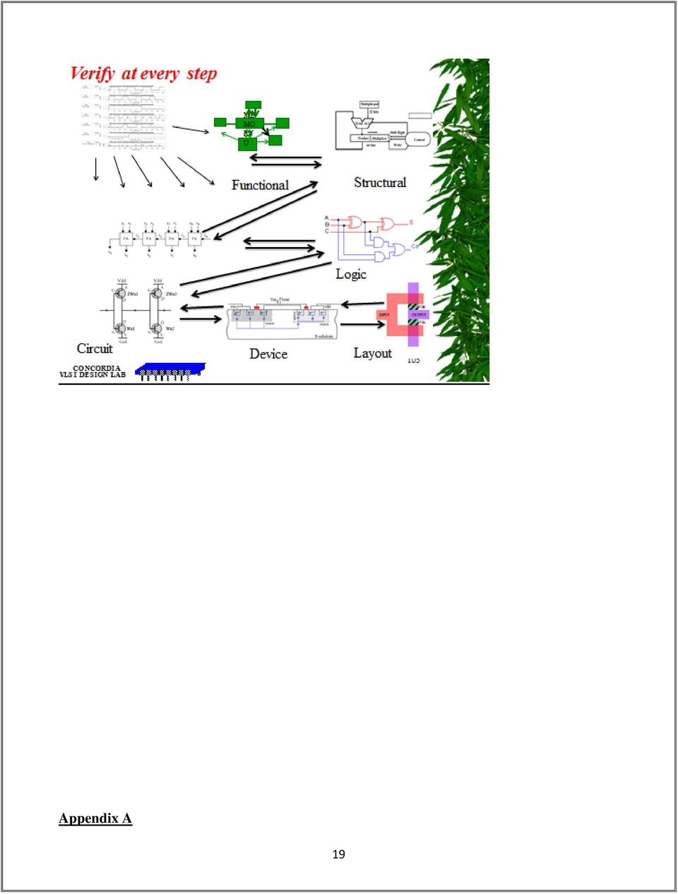
1 Digital Design and Synthesis INTRODUCTION The advances in digital design owe its progress to 3 factors. First the acceleration at which the CMOS technology has advanced in last few decades and the way that information has been stored and processed. Secondly, the driver for digital design has been the ability to treat all kinds of media as digital data that is stored, processed and manipulated and finally combining and storing all sorts of information and data in a single document and the third parameter is, the transmission in high speed over long distances. These concepts increased the requirement for digital design and ways to optimise its performance. Behavioural Systems Algorithms Register transfer Logic Transfer function Algorithmic Micro architecture Logic Circuit Rectangles Cells Macro-cells Modules Chips, boards Physical Processor ALU, registers Gates, F/Fs Transistors Structural Hardware modules Fig.1 Design description levels 1

2 Digital system and its design can be described in three domains namely: Behavioural, Structural and Physical domains as shown in Fig.1. In each domain, the level of description and decision to be taken and the complexity are different. The behavioural description is usually language based and can be pure algorithmic or signal flow graphs or even a transfer function and more likely a HDL Code. For example a multiplier can be described by A * B = C. At the behavioural level we may decide in using a serial or a parallel multiplier. So trade offs for speed, cost, chip area, power consumption etc. is made in this level. Many high level details are decided upon while the lower level details are compromised. Important design decisions such as what algorithm to be used for the system at hand are made at this level. It is important to know that the reward for optimization at this level is many folds of that of other levels as shown in Fig. 2. The digital designer starts the design at the conceptual level working with high level behavioural blocks and proceeds to design of major functional blocks that supports a given design specification. In order to manage complexity, the overall design may be partitioned and each partition dealt with separately using detailed structural constructs. In any case major decisions regarding algorithms, functional partitioning, structural partitioning and data transmission methods are made at this level while for each individual item optimising the speed, power consumption, area, and cost are identified. The benefit to the designer is that it provides a fast and accurate way to verify whether the concept is correct and design specification can be met and also provides means by which a compromise is reached between several objectives by WHAT IF ANALYSIS. The behavioural analysis is used usually for PROOF OF CONCEPT. 2

3 Optimization Levels Level Transformation Expected Power Saving Algorithmic Algorithm selection Orders of magnitude Behavioural Concurrency Several times Register Transfer Level Structural transformations ~10-15% Clock control ~10-90% Data/signal encoding ~20% Technology independent Extraction/decomposition ~15% Technology dependant Technology mapping ~20% Gate sizing ~20% Layout Placement 20% Fig-2 The behavioural model is usually converted to RTL level in HDL or block diagram usually manually. At the structural level, we are dealing with data paths, practical logic blocks and their interconnection. We may want to decide upon Dynamic logic or Static logic, Serial or Parallel input registers, what kind of adder to be used, what kind of multiplier will meet our speed and area, what is our clocking strategy etc. Our project for this course this year will based on Structural level, where you would design and code a multiplier in VHDL at structural level and then synthesise it to an FPGA. At the Structural level we use the EDA tools fully. At this level, The synthesis tools convert the blocks to gate level netlist and the logic synthesis tools optimize logic level design and the timing tools verify operations in terms of spec. requirement of timing, area and power. At the physical level, we will try to design and implement the circuit on chip. (COEN 6511) where our variables will be at silicon level. At this level the netlist is input to the EDA tools such as place and route which produces a layout, The layout is extracted and fed again for verification through an iterative process. Once a final satisfaction with the spec is acheived the layout is ready for download for fabrication. For example, how the chip layout is arranged, where the pads will be located, and how the Vdd and Vss are distributed and how the boards are arranged, where are the components placed etc. 3

4 The Y chart of Fig. 1 shows that one can make a de-composition and a transition from behavioural level to structural level. This can be achieved manually or through silicon compilation. By the same token one can transform from structural level to gate and logic level by creating FFs, gates, and higher blocks such as registers, counters, all kinds of modules. Also one can transcend to the physical level to design the transistors that make up the gates and step further to the polygons of different materials that make the transistors. So one can start automatically or manually to transcend from behavioural to the physical level. Silicon compilers do exist that accept behavioural level description and proceed to the physical chip, or chip layout. In all cases HDL language ie VHDL/ Verilog or others high languages is a good starting point to describe the system at hand. Generalizing then, logical synthesis is a structural form where the physical synthesis leads to the physical domain. Thus the design process includes the behavioural description followed by the decomposition of high level constructs into more precise functional units which are then mapped into the physical elements. The logical circuits that are commonly used are available as integrated circuits and are referred to as standard chips (in our design they are referred to as library cells). The advent of the very large scale integration (VLSI) has made the configuration on chip possible where a complete system can be designed synthesized and placed on a single chip. As complexity of the chips is increased to billions of transistors on a chip, then design automation becomes necessary. Designers now can design large chips verify it, automatically place and route it, re-evaluate its characteristic, debug it and verify its final functions before downloading the bitmap file on the actual chip as Shown in Fig. 4. One must always that these tools depend on the input and the rule of garbage in garbage out still applies. In general nowadays HDL is used extensively in digital design. The advantages are many including the design at the HDL level does not depend on any fabrication technology. Synthesis tools are available for converting the HDL to gate level netlist. The HDL is adaptable to new technologies, eliminating need for redesign. The verification tools at any step insure that all bugs are cleared and the design once goes to production is correct producing the exact requirement first time. Finally HDL, VHDL/Verilog/or higher level languages are becoming the 4

5 only method being used by designers. Currently the trend is to use structural design at the RTL level. In general two basic types of methodologies can be defined namely top-down design and bottomup design methodology. In top-down design methodology the top block is defined and then the sub-blocks necessary are identified in order to build a top level block. These are then further divided in progression into smaller units till we reach the leaf cells that cannot be divided further. The design is described in HDL and the HDL coding techniques will be applied to the design so that the design is modelled effectively and efficiently. Design errors that are obvious are checked through the preliminary synthesis of each HDL code and every block is verified before integrating it into a larger unit. Design process A design starts always with a specification. The specification describes what the circuit must do, but not how it is done. The specification is usually set by the customer who wants the final product. Once the designer knows what the circuit must do, she/he can begin to determine how it is done, for example, defining what are the inputs to the unit and the outputs that must be generated is a good first step. The designer then starts with translating the design specification into behavioural description, then decomposing the high level constructs into functional units and finally, then mapping these units into physical elements as shown in Fig.3. 5

6 Design Process: It starts with behavioural description, decomposing the high level of constructs into more precise functional units, then mapping these units into physical elements. System Specification Architectural Design (behavioural) Analysis Design Implementation (structural) Analysis Design Implementation (Physical) Analysis Fig. 3 A simple example of word specification from a customer may be as follows: Required an 8 bit microprocessor, no cache, simple addressing mode, 8 internal registers, Instruction word 8 bits, 8 bit address bus multiplexed with data bus, 40 pin package, dual IP package and consuming less than 1 Watt. A simple diagram of the system is shown in Fig.4 The designer then gets to work as first step starting with block diagram, decomposes the overall system into components that are available in the library or to be designed. The block diagram below 6

7 MEMORY I/P CPU O/P CONTROL DMA Fig. 4 shows the behavioural description of the system. Now each item is broken down to smaller units, for example, the CPU maybe broken into adder, multiplier, floating point unit etc. Now each unit in tern is broken down further using identifiable structures. For example an eight bits multiplier can be designed as shown in Fig.5 Fig. 5 An 8-bits multiplier While each adder is designed as shown in Fig. 6 below: 7

8 Fig. 6 A 1-bit adder This is a structured design where each unit is either designed specifically for this system or has been selected from the already available library. When the design of all the individual units have been completed then the overall design is simulated and compared to the specification. When the design meets the spec, then it is targeted to a physical implementation. As complexity of the chips is increased to billions of transistors on a chip, then design automation becomes necessary. Designers now can design large chips verify it, automatically place and route it, re-evaluate its characteristic, debug it and verify its final functions before downloading the bitmap file on the actual chip as Shown in Fig. 7 8

9 specification Description Behavioral HDL Description Gate-Level Netlist Logic Synthesis/ Proof of Concept Verification Verification Floor Planning/ Place & Route Verification/ Final Timing Implementation Fig. 7 Design Strategies Any system is comprised of many individual units such as boards, chips, power supply, routing etc. The success of the overall system depends on how well it is optimized in terms of performance, and at the end of the product cycle, what is the revenue that the newly designed system generates. This in turn depends on how well each individual unit in the system was designed through all its design levels from the algorithm down to the devices. For example how well a chip is designed is measured by several criteria such as functionality, speed, power, size etc. On the other hand other factors also play an important part such as time to design, time to market and ease of testing. The final implementation has to conform to the original spec. or better. During the design there are many factors that can be traded for the good design, therefore the knowledge of all factors affecting the design and their interdependence are important. 9

10 Most designs nowadays are large and complex. A successful designer has to structure his design and use design automation tools available. In general a successful designer uses the following 4 principals to achieve his design effectively and quickly. 1) Hierarchy 2) Regularity 3) Modularity 4) Locality Hierarchy, This is an extremely useful strategy when you have a complex system. It is the process of divide and conquer. The overall system is repeatedly divided into subunits and in turn the subunits are divided further until no further division is possible or the subunits are available in the library. At this stage the design is more manageable since the smaller sub-modules can be designed easier. The hierarchy can be in different domains in software or hardware modules. For example a VHDL entity module can be written or structurally designed in a hierarchical fashion. Parallel hierarchy is implemented in all domains. As an example a 4-bit adder can be designed by dividing the adder into 4 single bit adder, and an adder cab be designed using 2 half adders and so on as shown below: 10


11 Regularity Half adder Full Adder 4-bit Adder Regularity Although hierarchy can reduce complexity, however by applying regularity we can reduce complexity of the layout much further. This is because the method of simplify the work of the software that automates the design and in turn the design and implementation tasks are reduced. In this way, compact designs are obtained and finally verification of the design becomes simpler. 11

12 So at this stage we divide the hierarchy into smaller building blocks such that the small block can interlock in each other. For example an adder in a datapath design can be designed in a regular fashion in such a way that by concatenating the 1 bit of the adder n time an n bit adder is designed and implemented in layout directly. Vdd Cin Vss ao bo so co a b Vdd Cin Vss S C Vdd Co Vss Unit 1-bit Adder Vdd Cin Vss ao-a7 bo-b7 S0-S7 C7 a7 b7 s7 c7 Vdd Co Vss Vdd Cin Vss Modularity, 12

13 This is designing a module such that it is interface-able to other modules in the system. This means taking into consideration all the electrical, mechanical and physical parameters into account. The unit is verified and perfectly characterized. This is performed such that the module is well defined and ready for integration into most designs and understood and can be used by other members of the team or design community to be placed in the library. It basically gives confidence to the average designer since the module is well characterized. In general modularity makes implementation of design principal easy, Design principals: 1) Concatenation... physical abutments 2) Iteration... regular cells, arrays 3) Conditional selection...pla, Transistor selection Design of a Cell Additional buffers for easy interfacing to other modules which have certain input and output characteristic Locality This is a strategy to ensure that only components or routs that are essential to the module stay in the module, or by other definition optimization of internal components is very important because this will be used in the overall system, any local parameter should be kept within the module and close to where it is used to reduce for example resistance or capacitance. 13

14 VHDL, Due to complexity and speed of the design, designers have opted for design at higher level of abstraction. Designers follow functionality and let the Electronic Design Automation EDA, take care of the rest. The EDA tools are complete packages that take care of A to Z of the design translation, optimization and implementation. Most designs nowadays are performed with the aid of high evel languages such as VHDL or Verilog. This is so because these languages are design entry point, Specification language, as well as design simulation design verification tools. Thus it is a complete package by which the designer starts the specification to the end point by which the final VHDL code can be translated and synthesized into an FPGA or semi custom design. The design once described can be simulated and iterated through the design cycle until the final specification targeting a device for implementation is met. The following figure shows that most of the design, specification, simulation and verification can be done through VHDL. 14

15 Design Specification English Prose V H D L Modeling the behavior Data Path Logic Design Transfer Function, Boolean Equations, Flow Graphs, Pseudo Codes Computational Units,Registers, Buses Flip Flops, Gates, Netlist Netlist, ASCII text describing gates or library modules and their interconnection Implementation is vendor dependent ASIC FPGA Transistors, Wires Masks Manufacturing 4 At each point the Synthesis tools will provide you a report to check the design and its performance in terms of Speed, Area and Power. At anytime also the designer can go back and change its design thus repeating the design process. The following diagrams show the output from the synthesis reports. At the end of this course you will be doing your project. That requires design of a digital system, coding its behaviour at the structural level, writing the test bench, simulating the design and verifying its functionality as well as obtaining its performance. 15


16 Synthesis report Timing Report After Synthesis 16


17 Area report after Synthesis Power report after Synthesis 17

18 The Design process 18


19 Appendix A 19
20 By: Harish Harish prepared for COEN 6501 The following Appendix, shows the design concept using VHDL in details. VHDL DESIGN CONCEPT The behaviour and structure of the digital circuits are described by Hardware description language which is also used to simulate the circuit and check its response. VHDL language which is a simulation and verification language is basically used as a modelling language for digital systems for many tools it is used as an intermediate form of design entry. VHDL is not case sensitive and should be saved with an extension of.vhd. In a VHDL language the basic building blocks is known as module which describes the corresponding hardware module. A basic module structure may include declarations, statements, tasks and functions among others. VHDL uses the ASCII character set. The lexical elements for the language include identifier and reserve words special symbols etc. The general structure of VHDL module is an entity description which is followed by the description of the architecture. In the entity description the input and the output signals are declared and in the architecture description the internal operations of the module is specified. Entity Architecture Entity architecture Module 1 Entity architecture Module 2 Entity architecture Module N Figure 2: VHDL programme structure [1] The name of the module is given by the entity declaration (here two gates with respect to the figure).the entity description of the module represents the interconnections from this module to 20

21 the external interface. The port declaration specifies the inputs and outputs to the module (here A, B and D are inputs signals and E is the output signal). The name of the architecture associated with module is given by the architecture (here it is gates). The beginning and the end of the module is represented by the concurrent statements begin and end. A B D E Figure 3: VHDL module with two gates [1] entity two_gates is port (A, B, D: in bit; E: out bit); end two_gates architecture gates of two_gates is signal C: bit; begin C<= A and B; E<=C or D;?1? end gates; In addition to the in and out modes two other modes are being used buffer and linkage. The inout mode and the buffer mode are similar and it is useful if the signal is really an output signal. When we want to connect a VHDL entity to a non-vhdl entity a linkage port is useful. As both of these modes involve strict restrictions these are used at a restricted level. In VHDL there are 21
22 two types of delays which can be found-transport delays and inertial delays. Inertial delay which is default delay is intended to model gats and to those devices which do not propagate short pulses from input to output. The other VHDL delay which is the transport delay is intended to model the delay introduced by the wiring, in other words it simply delays an input signal by a specified delay time. Modelling this delay can be done by simply using the keyword transport in the code. This simulation related delays like inertial delay can inhibit many output change. Compilation and simulation of VHDL code In order to verify the implement the intended design correctly and also to verify if the design meets the specification simulation of the VHDL code is necessary. Accordingly there are three phases in the simulation of the VHDL code: compilation, elaboration and simulation. Resource library Simulator commands Compiler Intermediate Code Working library Elaborator simulation data structure Simulator Simulator output Figure 4: Compilation and Simulation of VHDL code [1] The syntax of the typed VHDL source code is verified to check if it adheres to the syntax and the semantic rules by the compiler also called as the analyser. On a positive result the compiler generates an intermediate code used by the simulator. In the elaboration process the VHDL intermediate code is converted to a form used by the simulator. The simulator process consists 22
23 of an initialisation phase and actual simulation. The simulator produces the desired simulation outputs upon accepting the simulation commands. The initial value to the signal is given and the corresponding actions are scheduled by the process of scheduling a transaction. In order to facilitate the correct initialisation process an initial value can be assigned in the VHDL module. Depending upon the type of the signal some initial value is assigned in the absence of an initial value. Simulation time is set to zero and the process is executed for corresponding transactions. Basically in a simulator whenever a component changes the output is scheduled to change after specified delay. The output change is specified when the simulated time is advanced to the next time when all the input changes have been processed. entity simulation_example is end simulation_example; architecture test1 of simulation_example is signal A, B: bit; begin P1: process (B) begin A<= 1 ; A<=transport 0 after 5 ns; end process P1; P2: process (A) begin if A= 1 then B<=not B after 10ns; end if; end process P2; end test1;?1? 23
24 VHDL data types and operators In VHDL there are several predefined data types which are used by the signals or they can also be user defined data type. Some of the data types are bit (0 or 1), Boolean (FALSE or TRUE), integer (in the range of (2 31-1) to + (2 31-1)), real (floating point number), character (any legal VHDL character), time (any integer with the units if fs, ps, ns, us, ms, sec, min, or hr). A common example of the user defined data type that is the data type created by the user is the enumeration type. In VHDL signals and variables cannot be mixed in the same assignment statement. Predefined VHDL operators are available and are grouped into seven classes- Binary logical operators, relational operators, shift operators, adding operators, unary operators, multiplying operators, miscellaneous operators. The operators in class seven gets the highest precedence when the parenthesis are not used and are applied first which is then followed by class six and then class five and so on. When operators of the same class are used they get precedence from left to right and the order of the precedence can be changed by the application of parenthesis. In the following expression (A & not B or C ror 2 and D) = In the above relative expression, the operators are applied in the order Not, &, ror, or, and, = Lexical description The VHDL text file is consisted of one or more text design files which must be prepared only from the prescribed ASCII character set. Character set There are various character set which are allowed in the design file. Furthermore there lot of characters which are included in the ASCII code representation to express like hexadecimal. Lexical elements 24
25 A sequence of characters that makes up a fundamental element which cannot be divided into smaller elements is called as lexical elements. The types of lexical elements: delimiter, identifier, comment, character literal, string literal, bit string literal, abstract literal. The separators are those which are used in between first lexical elements and after the last lexical elements. Many separators can be used in between the lexical elements. Delimiters The character that is used in order to separate the lexical elements is called as delimiter. All statements in VHDL are terminated using a ; character. The sequence of two delimiters is referred to as compound delimiter- =>, **,:=, /=, >=, <>, --. The use of delimiters reduces the use of specific separators in between the lexical characters. Character literal When a lexical element is formed by inserting one character between two apostrophe delimiter, it is known as character literal. String literal The lexical element formed by the insertion of sequence of graphical characters between two quotation delimiters is called a string literal. Since it is a lexical element the string literal is typed in one line. The number of characters in the sequence gives the length of the string literal. Bit string literal A lexical element which consists of a string of digits enclosed by the quotation character delimiters and preceded by base specifier is called as bit string literal. The base specifier is one of the letters like B-binary, O-octal, X-hexadecimal. The string of bits gives the value of a bit string literal. The association of this to a numerical value is dependent on the user. Decimal literal 25
26 An abstract literal which is used in many high level computer languages, expressed in standard decimal notation is called as a decimal literal. The exponential part of the literal is proceeded by letter E and only real literal accept the negative exponents value. Data types The specifications of values the object might have and the limitation of the types of operation the object of that type needs to perform is indicated by the data type. It is named set of values. A subtype is a type along with a constraint. If it is a legitimate value for the type and if the constraint is satisfied, the value belongs to the subtype. The type from which it was constructed is called the base type of the subtype. There are two classifications- scalar and composite. SCALAR DATA TYPES In scalar data types, the data types have single, simple values. An integer data type may have value of 15. This includes enumeration data types, numeric data types and physical data types. Enumeration types An enumeration type is a scalar type in which the values are defined by simply ordering them in a list. The elements may be identifiers or character literals. The two values for type bit are 0 and 1. Built in type for Boolean includes values TRUE or FALSE and for logical operators it is not, or, and and xor. A pre-defined attribute is the one which the value function in the range is associated with. The user-defined attribute is the one in which the attribute value is defined by the user. Its general form is attribute ATTRIBUTE_NAME:ATTRIBUTE_SUBTYPE; Numeric data types Built-in numeric data types Integer and Real with its associated performance of addition, subtraction, multiplication and division are present in VHDL language. The example for predefined numeric data-types Type Integer is range ; Type Real is range ;?2? 26
27 The ranges of the real and integer data types are implementation dependent which is in the range of to The user-defined data types are constrained numeric data types as the declaration constraints the range. The examples of user defined data types- Type COUNTER is range 0 to 100?2? Physical data types A scalar numeric data type which is associated to a system of units and is used to represent entities subject to physical measurements such as time, length, voltage, current is called as physical data type. The only pre-defined data type is time which is represented as Type TIME is range ; The ranges of physical data types are restricted by implementations. The declaration of any physical data type is allowed by an implementation which is in the range of to When the range is within these limits any user-defined data type may have three units as multiples of the next lower unit. Examples Type RESISTANCE is range 0 to Integer high Type POWER is range 0 to le19?2? COMPOSITE DATA TYPES The composite data types have complex values and have several components associated with it and it also represents an array of values with some relationship to one another. Arrays The data type in which each element has the same subtype i.e. homogeneous elements is called as an array. There are generally two predefined array types namely string and Bit_Vector. The former is used to define a character of elements and the latter is used to define an array of bits. They are- Type string is array (positive range <>) of character; Type Bit_Vector is array (natural range <>) of bit;?2? 27
28 Here the notation <> means the range is unconstrained, which indicates the user must specify the range when declaring the object. Both string and Bit_Vector are unconstrained and the user has to specify a range n positive for sting and in natural numbers for Bit_Vector. Some of the user defined array data types Type REGISTER_32_Bit is array (31 downto 0) of Bit; Subtype BITVECT3 is Bit_Vector (0 to 2); The REGISTER_32_Bit is a constrained array type which is descending in value. As the Bit vector is an unconstrained data type, subtypes with specific index ranges can be declared. BITVECT3 is a subtype of type Bit_Vector with an ascending index range 0 to 2. Declaration of data objects Before the referencing of the data types in assignment statement they must be declared. These declared objects are subsequently used in the further section for various other statements. Declaration of constants In declaration of the constants it is imperial that their values are specified. The constant name is separated from the type name by : delimiter and the type name is separated from a constant value by := delimiter. Some examples are- Constant ALPHA_LEVEL : PROBABILITY := 0.75; Constant INITIAL_STATE : STATE := S0; Constant END_MARKER : Character := DEL;?2? Declaration of variables In declaration of variable it must be seen that they are declared within a process or sub programme. The data type of the variable is specified by the variable declaration. In the declaration the values of the variables are specified if not the default value which is the left element in the type range specified in the declaration. Some examples are Variable STAR_COLOR, HAT_COLOR : COLOR; 28
29 Variable BETA_LEVEL : PROBABILITY := 0.0; Variable A, B, C, D : Bit; Variable R1, R2, R3, R4 : REG;?2? A, delimiter is used to in order to declare more than one variable of the same type. A : is used to separate the list of variable name from the data type and := is used to separate the initial value from the data type. Declaration of signals The signal declaration is similar to variable declaration. The signals are not be declared in processes or in sub programmes but it can be declared as ports in entity declaration or in the declarative region of architecture declarations. Some examples are --- Signal X1, X2, X3, X4, X5: Bit; Signal SR1, SR2, SR3, SR4: REG; Signal DOWN_COUNT: COUNTER := COUNTER right;?2? VHDL libraries The functionality of the VHDL is extended by the use of VHDL libraries and packages in defining types, functions, components and overloaded operators. Overloaded functions are generally created to handle operations involving heterogeneous data types. The package IEEE.std_logic_1164 defines a standard logic type which has nine values likewise std_logic_vectors defines logic vectors. Both the packages define overloaded arithmetic and logic operators for signed and unsigned numbers. VHDL IMPLEMENTATION Multiple forms of abstraction are possible. The same circuit can be implemented in different ways namely Structural model, Behavioral model and Mixed model. In the behavioral VHDL 29
30 description, the circuit or the system is defined at a high level of abstraction without implying any structure or technology specifying only the overall behaviour. The behavioral VHDL can also be implemented as dataflow or algorithmic level. In the data flow model data flow and control signals are specified. System working is specified in terms of data transfer between registers. DATA FLOW IMPLEMENTATION OF FULL ADDER architecture DATA_FLOW_IMPLEMENTATION of FULL_ADDER is block signal S1, S2, S3: BIT; begin S1 <= A xor B; SUM <= S1 xor CIN; S2 <= A and B; S3 <= S1 and CIN; COUT <= S2 or S3; end block; end DATA_FLOW_IMPLEMENTATION;?3? ALGORITHMIC IMPLEMENTATION OF FULL ADDER architecture ALGORITHMIC_IMPLEMENTATION of FULL_ADDER is block begin 30
31 process (A,B,CIN) variable S: BIT_VECTOR ( 1 to 3 ) := A & B & CIN; variable COUNT: INTEGER range 0 to 3 :=0; begin for i:= 1 to 3 loop if S(i) = 1 then COUNT := COUNT +1; end if ; end loop; case COUNT is when 0 => COUT <= 0 ; SUM <= 0 ; when 1 => COUT <= 0 ; SUM <= 1 ; when 2 => COUT <= 1 ; SUM <= 0 ; when 3 => COUT <= 1 ; SUM <= 1 ; end case; end process; end block; end ALGORITHIC-IMPLEMENTATION;?3? On the other hand in the implementation of the structural model which has a low level of abstraction the components used and the interconnection between the components are clearly specified. The structural model implementations are detailed enough to specify the use of particular gates and flip-flops from specific libraries/packages. 31
32 STRUCTURAL IMPLEMENTATION OF FULL ADDER architecture GATE_IMPLEMENTATION of FULL_ADDER is Block component or_gate port (A,B : in BIT; C: out BIT); end component; component and_gate port (A,B : in BIT; C: out BIT); end component; component xor_gate port (A,B : in BIT; C: out BIT); end component; signal S1, S2, S3: BIT; begin X1: xor_gate port map (A, B, S1); X2: xor_gate port map (S1, CIN, SUM); A1: and_gate port map (CIN, S1, S2); A2: and_2 port map (A, B, S3); O1: or_gate port map (S2, S3, COUT); end Block; end GATE_IMPLEMENTATION ;?3? Behavioral and structural design techniques are often combined giving rise to mixed VHDL implementation. Here different techniques are used to design different parts of the module. The automation tools generate efficient hardware hence they designed using behavioral level. Manual 32
33 optimisation needed by the memory structures are done through structural design as opposed to the behavioral modelling. MIXED IMPLEMENTATION OF FULL ADDER architecture MIXED_IMPLEMENTATION of FULL_ADDER is signal WIRE: BIT; component XOR_G port ( X1, X2: in BIT; XO1: out BIT); end component; for all: XOR_G use XOR_GATE(BEHAVIORAL); begin XOR1: XOR_G port map (X,Y,WIRE); XOR2: XOR_G port map (WIRE,CIN,SUM); COUT <= (WIRE and CIN) or (X and Y); end MIXED_IMPLEMENTATION?3? SEQUENTIAL CIRCUITS AND VHDL IMPLEMENTATION A combinational circuit is the one which produces its output based on the current inputs while a sequential circuit generates the outputs based on the current inputs and the previous states, which imply that memory, latches and flip-flops are common sequential circuits. The sequential logic responds to changes dependent on the clock. The primitives are required to model selective activity conditional on clock, edge triggered devices, sequences of operation in the process of modelling sequential circuits. 33
34 Shift register A shift register shifts the data either to the left or to the right through a number of cascaded flipflops. The VHDL code shows the shift register with a shift right function through eight flipflops. In the code the lines 13 and 14 asynchronously resets the flip-flops while lines 15 and 16 shift right the flip-flop when rising edge of the clock CLK occurs. Line 19 gives the SO output directly to FF8. library IEEE; use IEEE.std_logic_1164.all; entity SHIFTR is port (CLK, RSTn, SI: in std_logic; SO: out std_logic); end SHIFTR; architecture RTL of SHIFTR is signal FF8: std_logic_vector (7 downto 0); begin posedge: process (RSTn, CLK) begin if (RSTn, CLK) begin if (RSTn = 0 ) then FF8<= (FF8 range => 0 ); elseif (CLK event and CLK = 1 ) then FF8 <=SI&FF8 (FF8 length-1 downto 1); 34
35 end if; end process; SO <=FF8 (0); end RTL;?4? SI SO FD2 FD2 FD2 FD2 FD2 FD2 FD2 FD2 Figure 5: Synthesised schematic for shifter [2] COMBINATIONAL CIRCUITS AND VHDL IMPLEMENTATION The combinational circuits can be modelled by the VHDL by the use of concurrent statements. These concurrent statements are those which are ready to be executed and which get evaluated any time and also every time when the signal on the right side of the statement changes. VHDL assignment statements can be given as an example for concurrent statements. The right side of the concurrent statement is monitored by the VHDL simulator and when the signal changes the right side expression is immediately re-evaluated. After an appropriate delay the new value is assigned to the left side of the signal. The location of this concurrent statement in the programme is not important. Encoder An encoder converts one form of input pattern to a required form of output pattern. Here the encoder has a 4-bit input SEL and a 16-bit output Y. All the bits in the output will be 1, except the value represented by SEL. In the first VHDL code the programme uses if statement inside the process statement with the input SEL as process sensitivity list. 35
36 library IEEE; use IEEE.std_logic_1164.all; use IEEE.std_logic_unsigned.all; entity ENCODER is port (SEL: in std_logic_vector (0 downto 0) ;Y: out std_logic_vector (15 downto 0)) ; end ENCODER; architecture RTL of ENCODER is begin P0: process (SEL) begin Y <= (Y range => 1 ); if (SEL= 0000 ) then Y (0) <= 0 ; elseif (SEL= 0001 ) then Y (1) <= 0 ; elseif (SEL= 0010 ) then Y (2) <= 0 ; elseif (SEL= 0011 ) then Y (3) <= 0 ; elseif (SEL= 0100 ) then Y (4) <= 0 ; 36
37 elseif (SEL= 0101 ) then Y (5) <= 0 ; elseif (SEL= 0110 ) then Y (6) <= 0 ; elseif (SEL= 0111 ) then Y (7) <= 0 ; elseif (SEL= 1000 ) then Y (8) <= 0 ; elseif (SEL= 1001 ) then Y (9) <= 0 ; elseif (SEL= 1010 ) then Y (10) <= 0 ; elseif (SEL= 1011 ) then Y (11) <= 0 ; elseif (SEL= 1100 ) then Y (12) <= 0 ; elseif (SEL= 1101 ) then Y (13) <= 0 ; elseif (SEL= 1110 ) then Y (14) <= 0 ; else 37
38 Y (51) <= 0 ; end if; end process; end RTL; This coding uses a process statement and it includes conv_integer from the package IEEE std_logic_unsigned. architecture RTL of ENCODER is begin P3: process (SEL) begin Y <= (Y range => 1 ); Y (conv_integer (SEL)) <= 0 ; end process; end RTL;?4? PROGRAMMABLE LOGIC DEVICES Programmable logic devices helps in the removal of multiple off-the shelf devices and the inconvenience associated external wires. These devices allow an easy reprogramming and it is easier to change the design in case of error. They basically contain an array of basic building blocks that can be used to implement whatever functionality one desires. They differ in the building blocks or the amount of programmability they provide. 38
39 Programmable logic Factory programmable devices Field programmable devices ROM MPGA SPLD CPLD FPGA Read Only Memory Mask Programmable Gate Array Simple Programmable Logic Device Complex Programmable Logic Device Field Programmable Gate Array PROM PLA PAL GAL Programmable Read-Only Memory Programmable Logic Array Programmable Array Logic Generic Array Logic Figure 6: Major programmable logic devices [1] The field programmable logic devices are used in the programmer s user s field rather than a semi-conductor fab while the field programmable devices are programmed in a factory to meet the customers requirements. PAL s and PLA s contain arrays of gates allowing users to implement combinational function in two levels of gates. The special case of PLA is PAL wherein OR array is fixed and only AND array is programmable. They also may contain flipflops. The use of random access memory in Xilinx led to the creation of FPGA that integrate fairly a large amount of logic. 39
40 Simple programmable logic devices The early generation of programmable logic devices is collectively called simple programmable logic device. Read-Only Memory The read-only memory is built up of an array of semiconductor devices that are interconnected enabling it to store a binary data. The data that is stored in ROM is permanent and can be read out whenever wanted, but it cannot be changed under normal operating conditions. A ROM consists of a decoder and a memory array. When a pattern of n 1 s and 0 s are applied to the input the output obtained is exactly 2 n decoder output which is 1. In the memory the decoder output line selects one of the words and the bit pattern stored in the word is transferred to the memory output lines. Basically there many types of ROM namely- user programmable ROM s, erasable programmable ROM s, electrically erasable and programmable ROM s and flash memory. Programmable Logic Array A programmable logic array performs the same basic function as a ROM. An n input and n output PLA can realise m functions of n-variables. Basically the internal organisation of a PLA is different from that of ROM. In PLA the decoder is replaced with an AND array which is used to realise the selected product terms of the input variables. Meanwhile the OR array OR s the product terms together which is needed to form the output functions. The PLA may use NOR- NOR logic instead of AND-OR logic. Programmable Array Logic The PAL is a special case of programmable logic array in which the AND array is programmable and OR array is fixed. Structurally the PLA and the PAL resemble one another but PAL is less expensive than PLA as only the AND gate is programmable. In a PAL a buffer is used as each input has to drive many AND gate inputs. In order to make the desired connections to the AND gate inputs some of the interconnection points are programmed while programming the PAL. Unlike the general PLA each function must be realised and simplified by itself without regard to common terms as the AND gates cannot be shared with two or more OR gates. 40
41 Programmable Logic Devices With the improvement in the integrated technology the PAL s are enabled to be reprogrammable now called as PLD s. In addition to the AND OR arrays that the PAL s have the PLD s contains some multiplexers and some additional programmability and these are named with respect to their input and output capability. Typically the PLD s have some 8 to 12I/O pins. Further each output pin is connected to an output macrocell which has a D-flip flop connected to it. The programmable I/O pins can act as inputs or combinational or flip-flop outputs. One can find dedicated output clocks in some PLD s while others have a dual-purpose pin which can be used either as a clock or as an input. Tristate buffers are present in all the PLD s at the output. PALASM and ABEL are the two programming languages used in PAL s and PLD s. Complex programmable logic devices The developments in the IC technology have made it possible to create programmable ICs equal to several PLDs in the same chip referred to as complex programmable logic devices (CPLDs). When these are incorporated with storage elements digital systems are created in the IC. Basically a CPLD is an IC consisting of a number of PAL- like logic blocks together with a programmable interconnect matrix. The PLD are necessarily interconnected using a crossbar-like switch typically consisting of 500 to 10,000 logic gates. These CPLDs are electronically erasable and reprogrammable and hence called as EPLDs. There are number of macrocells that are present in a typical CPLD. An interconnection array is used to establish the connection between the function blocks. Each macrocell consists of a flip-flop and an OR gate that has its input connected to an AND gate array. Those CPLDs which are based on PALs has each OR gate which is associated with fixed set of AND gates and those CPLDs based on PLAs has AND gate output connected to any OR gate input in that block. The signal generated in functional block (PLA) is routed through a macrocell to an I/O pin. Any of the 36 inputs of the IA can be connected to any of the inputs of the 48 AND gates. Each OR gate has to accept upto 48 product term input from the AND array. The mux1 is programmed to select the OR gate output while the mux2 can be programmed to select their combinational output or flip-flop output. The output is fed to the interconnect array and to output cell which 41
42 includes the three-state buffer to drive the I/O pin. When the I/O is used as an input, the buffer must be disabled. Field programmable gate arrays FPGAs are ICs which contain an array of identical logic blocks that are provided with programmable interconnections. There are number of FPGA products available namely Xilinx, Altera, lattice, actel, cypress. Arrays of programmable logic blocks are distributed within the FPGA surrounded by input/output interface blocks. Basically there many types of programming blocks like multiplexers and logic gates on one hand while some use only transistors. The architecture also differs according to the use and purpose. The programmable blocks like logic block, interconnect help to re-programme FPGA. In FPGA them interconnect can be programmed to make or break connection. There might be different interconnects used depending upon the FPGA company like general purpose interconnect, direct interconnect, global lines and so on. StaticRAM programming technology, EPROM/EEPROM/flash programming technology, Antifuse programming technology are the programming technologies used to programme FPGA. In more recent times the vendors have incorporated embedded processors, dedicated multipliers, analog-to-digital converters and so on in FPGAs. VHDL SYNTHESIS ENVIRONMENT Designer analyser. The design analyser is a user interface tool which has a command window for the users in order to supply synthesis commands. VHDL compiler. The compiler parses VHDL code, checks for syntax errors and checks for VHDL construct in the code that are synthesizable. It also generates a summary report on the components used. Design compiler. The design is optimised by the design compiler based on the synthesis constraints such as speed and area requirements. 42
43 Design time. The design time is a timing analyser which is used to find the critical path and to perform timing checks. VHDL code Design analyser VHDL Compiler Design compiler Test compiler Design Time Timing Analysis Synthesis technology gate limited Netlist Place and route tools Figure 7: Synopsis synthesis tools [2] There are many commands in the directory for synthesis. Directory syn is used to run the synthesis, unix command design_analyser is used to bring synopsis design analyser. This also executes commands specified in the file.synopsys_dc.setup, and brings up the design window. The synthesis script file compile.report generates synthesis results to be placed in the REPORT directory. When both synopsis VHDL and synthesis tools use the same library there would be a time stamp delay so it is better to separate both the libraries. 43
44 A synthesis technology library consists of definitions of basic components, operating conditions and wire load models. Each component consists of its own logical function, timing, input pin loading and output pin drive information. The synthesis usually uses library_name.sdb. The command read/acct/synlib/isi/lca300k.db can be used to read the synthesis technology inside the designer analyser. It is important that we select a good synthesis library to match design objectives such as speed requirements, cost, production schedule, and design tools. REFERENCES 1. INTRODUCTION TO DIGITAL SYSTEMS: Modeling, Synthesis, and Simulation Using VHDL Mohammed Ferdjallah 2. Digital systems design using VHDL Charles H.Roth, Lizy Kurian John 3. Digital systems design and VHDL synthesis K.C.Chang 4. Prof. A.Alkhalili Notes 5. Verilog HDL: A Guide to Digital Design and Synthesis, Second Edition Samir Palnitkar 6. VHDL Design Representation and Synthesis, Second Edition James R. Armstrong, F. Gail Grey Figures [1] Digital systems design using VHDL Charles H.Roth, Lizy Kurian John [2] Digital systems design and VHDL synthesis K.C.Chang Examples and VHDL codes?1? Digital systems design using VHDL Charles H.Roth, Lizy Kurian John?2? VHDL Design Representation and Synthesis, Second Edition James R. Armstrong, F. Gail?3? Prof. A.Alkhalili Notes?4? Digital systems design and VHDL synthesis K.C.Chang 44
45 Design Test bench VHDL coding simulation Synthesis Target layout ASIC vendor for fabrication Fig. 1 Design Concept using VHDL 45
VHDL GUIDELINES FOR SYNTHESIS
 VHDL GUIDELINES FOR SYNTHESIS Claudio Talarico For internal use only 1/19 BASICS VHDL VHDL (Very high speed integrated circuit Hardware Description Language) is a hardware description language that allows
Modeling Sequential Elements with Verilog. Prof. Chien-Nan Liu TEL: 03-4227151 ext:34534 Email: jimmy@ee.ncu.edu.tw. Sequential Circuit
 Modeling Sequential Elements with Verilog Prof. Chien-Nan Liu TEL: 03-4227151 ext:34534 Email: jimmy@ee.ncu.edu.tw 4-1 Sequential Circuit Outputs are functions of inputs and present states of storage elements
Digital Systems Design! Lecture 1 - Introduction!!
 ECE 3401! Digital Systems Design! Lecture 1 - Introduction!! Course Basics Classes: Tu/Th 11-12:15, ITE 127 Instructor Mohammad Tehranipoor Office hours: T 1-2pm, or upon appointments @ ITE 441 Email:
ECE 3401 Lecture 7. Concurrent Statements & Sequential Statements (Process)
") ECE 3401 Lecture 7 Concurrent Statements & Sequential Statements (Process) Concurrent Statements VHDL provides four different types of concurrent statements namely: Signal Assignment Statement Simple Assignment
ECE 3401 Lecture 7 Concurrent Statements & Sequential Statements (Process) Concurrent Statements VHDL provides four different types of concurrent statements namely: Signal Assignment Statement Simple Assignment
Sistemas Digitais I LESI - 2º ano
 Sistemas Digitais I LESI - 2º ano Lesson 6 - Combinational Design Practices Prof. João Miguel Fernandes (miguel@di.uminho.pt) Dept. Informática UNIVERSIDADE DO MINHO ESCOLA DE ENGENHARIA - PLDs (1) - The
Life Cycle of a Memory Request. Ring Example: 2 requests for lock 17
 Life Cycle of a Memory Request (1) Use AQR or AQW to place address in AQ (2) If A[31]==0, check for hit in DCache Ring (3) Read Hit: place cache word in RQ; Write Hit: replace cache word with WQ RDDest/RDreturn
RAPID PROTOTYPING OF DIGITAL SYSTEMS Second Edition
 RAPID PROTOTYPING OF DIGITAL SYSTEMS Second Edition A Tutorial Approach James O. Hamblen Georgia Institute of Technology Michael D. Furman Georgia Institute of Technology KLUWER ACADEMIC PUBLISHERS Boston
if-then else : 2-1 mux mux: process (A, B, Select) begin if (select= 1 ) then Z <= A; else Z <= B; end if; end process;
 begin if (select= 1 ) then Z <= A; else Z <= B; end if; end process;") if-then else : 2-1 mux mux: process (A, B, Select) begin if (select= 1 ) then Z
if-then else : 2-1 mux mux: process (A, B, Select) begin if (select= 1 ) then Z
Digitale Signalverarbeitung mit FPGA (DSF) Soft Core Prozessor NIOS II Stand Mai 2007. Jens Onno Krah
 Soft Core Prozessor NIOS II Stand Mai 2007. Jens Onno Krah") (DSF) Soft Core Prozessor NIOS II Stand Mai 2007 Jens Onno Krah Cologne University of Applied Sciences www.fh-koeln.de jens_onno.krah@fh-koeln.de NIOS II 1 1 What is Nios II? Altera s Second Generation
(DSF) Soft Core Prozessor NIOS II Stand Mai 2007 Jens Onno Krah Cologne University of Applied Sciences www.fh-koeln.de jens_onno.krah@fh-koeln.de NIOS II 1 1 What is Nios II? Altera s Second Generation
Aims and Objectives. E 3.05 Digital System Design. Course Syllabus. Course Syllabus (1) Programmable Logic
 Programmable Logic") Aims and Objectives E 3.05 Digital System Design Peter Cheung Department of Electrical & Electronic Engineering Imperial College London URL: www.ee.ic.ac.uk/pcheung/ E-mail: p.cheung@ic.ac.uk How to go
Aims and Objectives E 3.05 Digital System Design Peter Cheung Department of Electrical & Electronic Engineering Imperial College London URL: www.ee.ic.ac.uk/pcheung/ E-mail: p.cheung@ic.ac.uk How to go
Chapter 7 Memory and Programmable Logic
 NCNU_2013_DD_7_1 Chapter 7 Memory and Programmable Logic 71I 7.1 Introduction ti 7.2 Random Access Memory 7.3 Memory Decoding 7.5 Read Only Memory 7.6 Programmable Logic Array 77P 7.7 Programmable Array
Quartus II Software Design Series : Foundation. Digitale Signalverarbeitung mit FPGA. Digitale Signalverarbeitung mit FPGA (DSF) Quartus II 1
 Quartus II 1") (DSF) Quartus II Stand: Mai 2007 Jens Onno Krah Cologne University of Applied Sciences www.fh-koeln.de jens_onno.krah@fh-koeln.de Quartus II 1 Quartus II Software Design Series : Foundation 2007 Altera
(DSF) Quartus II Stand: Mai 2007 Jens Onno Krah Cologne University of Applied Sciences www.fh-koeln.de jens_onno.krah@fh-koeln.de Quartus II 1 Quartus II Software Design Series : Foundation 2007 Altera
Chapter 2 Logic Gates and Introduction to Computer Architecture
 Chapter 2 Logic Gates and Introduction to Computer Architecture 2.1 Introduction The basic components of an Integrated Circuit (IC) is logic gates which made of transistors, in digital system there are
Introduction to Programmable Logic Devices. John Coughlan RAL Technology Department Detector & Electronics Division
 Introduction to Programmable Logic Devices John Coughlan RAL Technology Department Detector & Electronics Division PPD Lectures Programmable Logic is Key Underlying Technology. First-Level and High-Level
LAB #3 VHDL RECOGNITION AND GAL IC PROGRAMMING USING ALL-11 UNIVERSAL PROGRAMMER
 LAB #3 VHDL RECOGNITION AND GAL IC PROGRAMMING USING ALL-11 UNIVERSAL PROGRAMMER OBJECTIVES 1. Learn the basic elements of VHDL that are implemented in Warp. 2. Build a simple application using VHDL and
Chapter 4 Register Transfer and Microoperations. Section 4.1 Register Transfer Language
 Chapter 4 Register Transfer and Microoperations Section 4.1 Register Transfer Language Digital systems are composed of modules that are constructed from digital components, such as registers, decoders,
A Verilog HDL Test Bench Primer Application Note
 A Verilog HDL Test Bench Primer Application Note Table of Contents Introduction...1 Overview...1 The Device Under Test (D.U.T.)...1 The Test Bench...1 Instantiations...2 Figure 1- DUT Instantiation...2
Design of a High Speed Communications Link Using Field Programmable Gate Arrays
 Customer-Authored Application Note AC103 Design of a High Speed Communications Link Using Field Programmable Gate Arrays Amy Lovelace, Technical Staff Engineer Alcatel Network Systems Introduction A communication
University of St. Thomas ENGR 230 ---- Digital Design 4 Credit Course Monday, Wednesday, Friday from 1:35 p.m. to 2:40 p.m. Lecture: Room OWS LL54
 Fall 2005 Instructor Texts University of St. Thomas ENGR 230 ---- Digital Design 4 Credit Course Monday, Wednesday, Friday from 1:35 p.m. to 2:40 p.m. Lecture: Room OWS LL54 Lab: Section 1: OSS LL14 Tuesday
ECE232: Hardware Organization and Design. Part 3: Verilog Tutorial. http://www.ecs.umass.edu/ece/ece232/ Basic Verilog
 ECE232: Hardware Organization and Design Part 3: Verilog Tutorial http://www.ecs.umass.edu/ece/ece232/ Basic Verilog module ();
Introduction to Digital System Design
 Introduction to Digital System Design Chapter 1 1 Outline 1. Why Digital? 2. Device Technologies 3. System Representation 4. Abstraction 5. Development Tasks 6. Development Flow Chapter 1 2 1. Why Digital
ECE410 Design Project Spring 2008 Design and Characterization of a CMOS 8-bit Microprocessor Data Path
 ECE410 Design Project Spring 2008 Design and Characterization of a CMOS 8-bit Microprocessor Data Path Project Summary This project involves the schematic and layout design of an 8-bit microprocessor data
CHAPTER 3 Boolean Algebra and Digital Logic
 CHAPTER 3 Boolean Algebra and Digital Logic 3.1 Introduction 121 3.2 Boolean Algebra 122 3.2.1 Boolean Expressions 123 3.2.2 Boolean Identities 124 3.2.3 Simplification of Boolean Expressions 126 3.2.4
9/14/2011 14.9.2011 8:38
 Algorithms and Implementation Platforms for Wireless Communications TLT-9706/ TKT-9636 (Seminar Course) BASICS OF FIELD PROGRAMMABLE GATE ARRAYS Waqar Hussain firstname.lastname@tut.fi Department of Computer
The Designer's Guide to VHDL
 The Designer's Guide to VHDL Third Edition Peter J. Ashenden EDA CONSULTANT, ASHENDEN DESIGNS PTY. LTD. ADJUNCT ASSOCIATE PROFESSOR, ADELAIDE UNIVERSITY AMSTERDAM BOSTON HEIDELBERG LONDON m^^ yj 1 ' NEW
INTRODUCTION TO DIGITAL SYSTEMS. IMPLEMENTATION: MODULES (ICs) AND NETWORKS IMPLEMENTATION OF ALGORITHMS IN HARDWARE
 AND NETWORKS IMPLEMENTATION OF ALGORITHMS IN HARDWARE") INTRODUCTION TO DIGITAL SYSTEMS 1 DESCRIPTION AND DESIGN OF DIGITAL SYSTEMS FORMAL BASIS: SWITCHING ALGEBRA IMPLEMENTATION: MODULES (ICs) AND NETWORKS IMPLEMENTATION OF ALGORITHMS IN HARDWARE COURSE EMPHASIS:
INTRODUCTION TO DIGITAL SYSTEMS 1 DESCRIPTION AND DESIGN OF DIGITAL SYSTEMS FORMAL BASIS: SWITCHING ALGEBRA IMPLEMENTATION: MODULES (ICs) AND NETWORKS IMPLEMENTATION OF ALGORITHMS IN HARDWARE COURSE EMPHASIS:
VHDL Test Bench Tutorial
 University of Pennsylvania Department of Electrical and Systems Engineering ESE171 - Digital Design Laboratory VHDL Test Bench Tutorial Purpose The goal of this tutorial is to demonstrate how to automate
Chapter 13: Verification
 Chapter 13: Verification Prof. Ming-Bo Lin Department of Electronic Engineering National Taiwan University of Science and Technology Digital System Designs and Practices Using Verilog HDL and FPGAs @ 2008-2010,
Architectures and Platforms
 Hardware/Software Codesign Arch&Platf. - 1 Architectures and Platforms 1. Architecture Selection: The Basic Trade-Offs 2. General Purpose vs. Application-Specific Processors 3. Processor Specialisation
MICROPROCESSOR. Exclusive for IACE Students www.iace.co.in iacehyd.blogspot.in Ph: 9700077455/422 Page 1
 MICROPROCESSOR A microprocessor incorporates the functions of a computer s central processing unit (CPU) on a single Integrated (IC), or at most a few integrated circuit. It is a multipurpose, programmable
Agenda. Michele Taliercio, Il circuito Integrato, Novembre 2001
 Agenda Introduzione Il mercato Dal circuito integrato al System on a Chip (SoC) La progettazione di un SoC La tecnologia Una fabbrica di circuiti integrati 28 How to handle complexity G The engineering
7a. System-on-chip design and prototyping platforms
 7a. System-on-chip design and prototyping platforms Labros Bisdounis, Ph.D. Department of Computer and Communication Engineering 1 What is System-on-Chip (SoC)? System-on-chip is an integrated circuit
Memory Systems. Static Random Access Memory (SRAM) Cell
 Cell") Memory Systems This chapter begins the discussion of memory systems from the implementation of a single bit. The architecture of memory chips is then constructed using arrays of bit implementations coupled
Memory Systems This chapter begins the discussion of memory systems from the implementation of a single bit. The architecture of memory chips is then constructed using arrays of bit implementations coupled
Fault Modeling. Why model faults? Some real defects in VLSI and PCB Common fault models Stuck-at faults. Transistor faults Summary
 Fault Modeling Why model faults? Some real defects in VLSI and PCB Common fault models Stuck-at faults Single stuck-at faults Fault equivalence Fault dominance and checkpoint theorem Classes of stuck-at
Flip-Flops, Registers, Counters, and a Simple Processor
 June 8, 22 5:56 vra235_ch7 Sheet number Page number 349 black chapter 7 Flip-Flops, Registers, Counters, and a Simple Processor 7. Ng f3, h7 h6 349 June 8, 22 5:56 vra235_ch7 Sheet number 2 Page number
Attaining EDF Task Scheduling with O(1) Time Complexity
 Time Complexity") Attaining EDF Task Scheduling with O(1) Time Complexity Verber Domen University of Maribor, Faculty of Electrical Engineering and Computer Sciences, Maribor, Slovenia (e-mail: domen.verber@uni-mb.si) Abstract:
Attaining EDF Task Scheduling with O(1) Time Complexity Verber Domen University of Maribor, Faculty of Electrical Engineering and Computer Sciences, Maribor, Slovenia (e-mail: domen.verber@uni-mb.si) Abstract:
SECTION C [short essay] [Not to exceed 120 words, Answer any SIX questions. Each question carries FOUR marks] 6 x 4=24 marks
![SECTION C [short essay] [Not to exceed 120 words, Answer any SIX questions. Each question carries FOUR marks] 6 x 4=24 marks](/thumbs/35/17285180.jpg "SECTION C [short essay] [Not to exceed 120 words, Answer any SIX questions. Each question carries FOUR marks] 6 x 4=24 marks") UNIVERSITY OF KERALA First Degree Programme in Computer Applications Model Question Paper Semester I Course Code- CP 1121 Introduction to Computer Science TIME : 3 hrs Maximum Mark: 80 SECTION A [Very
UNIVERSITY OF KERALA First Degree Programme in Computer Applications Model Question Paper Semester I Course Code- CP 1121 Introduction to Computer Science TIME : 3 hrs Maximum Mark: 80 SECTION A [Very
Best Practises for LabVIEW FPGA Design Flow. uk.ni.com ireland.ni.com
 Best Practises for LabVIEW FPGA Design Flow 1 Agenda Overall Application Design Flow Host, Real-Time and FPGA LabVIEW FPGA Architecture Development FPGA Design Flow Common FPGA Architectures Testing and
ESP-CV Custom Design Formal Equivalence Checking Based on Symbolic Simulation
 Datasheet -CV Custom Design Formal Equivalence Checking Based on Symbolic Simulation Overview -CV is an equivalence checker for full custom designs. It enables efficient comparison of a reference design
The System Designer's Guide to VHDL-AMS
 The System Designer's Guide to VHDL-AMS Analog, Mixed-Signal, and Mixed-Technology Modeling Peter J. Ashenden EDA CONSULTANT, ASHENDEN DESIGNS PTY. LTD. VISITING RESEARCH FELLOW, ADELAIDE UNIVERSITY Gregory
1. True or False? A voltage level in the range 0 to 2 volts is interpreted as a binary 1.
 File: chap04, Chapter 04 1. True or False? A voltage level in the range 0 to 2 volts is interpreted as a binary 1. 2. True or False? A gate is a device that accepts a single input signal and produces one
Lecture 5: Gate Logic Logic Optimization
 Lecture 5: Gate Logic Logic Optimization MAH, AEN EE271 Lecture 5 1 Overview Reading McCluskey, Logic Design Principles- or any text in boolean algebra Introduction We could design at the level of irsim
E158 Intro to CMOS VLSI Design. Alarm Clock
 E158 Intro to CMOS VLSI Design Alarm Clock Sarah Yi & Samuel (Tae) Lee 4/19/2010 Introduction The Alarm Clock chip includes the basic functions of an alarm clock such as a running clock time and alarm
Lecture N -1- PHYS 3330. Microcontrollers
 Lecture N -1- PHYS 3330 Microcontrollers If you need more than a handful of logic gates to accomplish the task at hand, you likely should use a microcontroller instead of discrete logic gates 1. Microcontrollers
Quartus II Introduction for VHDL Users
 Quartus II Introduction for VHDL Users This tutorial presents an introduction to the Quartus II software. It gives a general overview of a typical CAD flow for designing circuits that are implemented by
Example-driven Interconnect Synthesis for Heterogeneous Coarse-Grain Reconfigurable Logic
 Example-driven Interconnect Synthesis for Heterogeneous Coarse-Grain Reconfigurable Logic Clifford Wolf, Johann Glaser, Florian Schupfer, Jan Haase, Christoph Grimm Computer Technology /99 Overview Ultra-Low-Power
Implementation of Web-Server Using Altera DE2-70 FPGA Development Kit
 1 Implementation of Web-Server Using Altera DE2-70 FPGA Development Kit A THESIS SUBMITTED IN PARTIAL FULFILLMENT OF THE REQUIREMENT OF FOR THE DEGREE IN Bachelor of Technology In Electronics and Communication
Digital Electronics Detailed Outline
 Digital Electronics Detailed Outline Unit 1: Fundamentals of Analog and Digital Electronics (32 Total Days) Lesson 1.1: Foundations and the Board Game Counter (9 days) 1. Safety is an important concept
GETTING STARTED WITH PROGRAMMABLE LOGIC DEVICES, THE 16V8 AND 20V8
 GETTING STARTED WITH PROGRAMMABLE LOGIC DEVICES, THE 16V8 AND 20V8 Robert G. Brown All Rights Reserved August 25, 2000 Alta Engineering 58 Cedar Lane New Hartford, CT 06057-2905 (860) 489-8003 www.alta-engineering.com
Finite State Machine Design and VHDL Coding Techniques
 Finite State Machine Design and VHDL Coding Techniques Iuliana CHIUCHISAN, Alin Dan POTORAC, Adrian GRAUR "Stefan cel Mare" University of Suceava str.universitatii nr.13, RO-720229 Suceava iulia@eed.usv.ro,
ETEC 2301 Programmable Logic Devices. Chapter 10 Counters. Shawnee State University Department of Industrial and Engineering Technologies
 ETEC 2301 Programmable Logic Devices Chapter 10 Counters Shawnee State University Department of Industrial and Engineering Technologies Copyright 2007 by Janna B. Gallaher Asynchronous Counter Operation
Digital Design with Synthesizable VHDL
 Digital Design with Synthesizable VHDL Prof. Stephen A. Edwards Columbia University Spring 2012 Combinational Logic in a Dataflow Style Hierarchy: Instantiating Components (entities) Combinational Logic
Hardware Implementation of the Stone Metamorphic Cipher
 International Journal of Computer Science & Network Security VOL.10 No.8, 2010 Hardware Implementation of the Stone Metamorphic Cipher Rabie A. Mahmoud 1, Magdy Saeb 2 1. Department of Mathematics, Faculty
Implementation Details
 LEON3-FT Processor System Scan-I/F FT FT Add-on Add-on 2 2 kbyte kbyte I- I- Cache Cache Scan Scan Test Test UART UART 0 0 UART UART 1 1 Serial 0 Serial 1 EJTAG LEON_3FT LEON_3FT Core Core 8 Reg. Windows
Testing of Digital System-on- Chip (SoC)
") Testing of Digital System-on- Chip (SoC) 1 Outline of the Talk Introduction to system-on-chip (SoC) design Approaches to SoC design SoC test requirements and challenges Core test wrapper P1500 core test
Testing of Digital System-on- Chip (SoC) 1 Outline of the Talk Introduction to system-on-chip (SoC) design Approaches to SoC design SoC test requirements and challenges Core test wrapper P1500 core test
Introduction to CMOS VLSI Design (E158) Lecture 8: Clocking of VLSI Systems
 Lecture 8: Clocking of VLSI Systems") Harris Introduction to CMOS VLSI Design (E158) Lecture 8: Clocking of VLSI Systems David Harris Harvey Mudd College David_Harris@hmc.edu Based on EE271 developed by Mark Horowitz, Stanford University MAH
Harris Introduction to CMOS VLSI Design (E158) Lecture 8: Clocking of VLSI Systems David Harris Harvey Mudd College David_Harris@hmc.edu Based on EE271 developed by Mark Horowitz, Stanford University MAH
COMBINATIONAL and SEQUENTIAL LOGIC CIRCUITS Hardware implementation and software design
 PH-315 COMINATIONAL and SEUENTIAL LOGIC CIRCUITS Hardware implementation and software design A La Rosa I PURPOSE: To familiarize with combinational and sequential logic circuits Combinational circuits
Digital Logic Design. Basics Combinational Circuits Sequential Circuits. Pu-Jen Cheng
 Digital Logic Design Basics Combinational Circuits Sequential Circuits Pu-Jen Cheng Adapted from the slides prepared by S. Dandamudi for the book, Fundamentals of Computer Organization and Design. Introduction
Asynchronous & Synchronous Reset Design Techniques - Part Deux
 Clifford E. Cummings Don Mills Steve Golson Sunburst Design, Inc. LCDM Engineering Trilobyte Systems cliffc@sunburst-design.com mills@lcdm-eng.com sgolson@trilobyte.com ABSTRACT This paper will investigate
DEPARTMENT OF INFORMATION TECHNLOGY
 DRONACHARYA GROUP OF INSTITUTIONS, GREATER NOIDA Affiliated to Mahamaya Technical University, Noida Approved by AICTE DEPARTMENT OF INFORMATION TECHNLOGY Lab Manual for Computer Organization Lab ECS-453
Introduction. Jim Duckworth ECE Department, WPI. VHDL Short Course - Module 1
 VHDL Short Course Module 1 Introduction Jim Duckworth ECE Department, WPI Jim Duckworth, WPI 1 Topics Background to VHDL Introduction to language Programmable Logic Devices CPLDs and FPGAs FPGA architecture
High-Level Synthesis for FPGA Designs
 High-Level Synthesis for FPGA Designs BRINGING BRINGING YOU YOU THE THE NEXT NEXT LEVEL LEVEL IN IN EMBEDDED EMBEDDED DEVELOPMENT DEVELOPMENT Frank de Bont Trainer consultant Cereslaan 10b 5384 VT Heesch
Von der Hardware zur Software in FPGAs mit Embedded Prozessoren. Alexander Hahn Senior Field Application Engineer Lattice Semiconductor
 Von der Hardware zur Software in FPGAs mit Embedded Prozessoren Alexander Hahn Senior Field Application Engineer Lattice Semiconductor AGENDA Overview Mico32 Embedded Processor Development Tool Chain HW/SW
Sequential Circuit Design
 Sequential Circuit Design Lan-Da Van ( 倫 ), Ph. D. Department of Computer Science National Chiao Tung University Taiwan, R.O.C. Fall, 2009 ldvan@cs.nctu.edu.tw http://www.cs.nctu.edu.tw/~ldvan/ Outlines
Lecture 7: Clocking of VLSI Systems
 Lecture 7: Clocking of VLSI Systems MAH, AEN EE271 Lecture 7 1 Overview Reading Wolf 5.3 Two-Phase Clocking (good description) W&E 5.5.1, 5.5.2, 5.5.3, 5.5.4, 5.5.9, 5.5.10 - Clocking Note: The analysis
CNC FOR EDM MACHINE TOOL HARDWARE STRUCTURE. Ioan Lemeni
 CNC FOR EDM MACHINE TOOL HARDWARE STRUCTURE Ioan Lemeni Computer and Communication Engineering Department Faculty of Automation, Computers and Electronics University of Craiova 13, A.I. Cuza, Craiova,
AC 2007-2485: PRACTICAL DESIGN PROJECTS UTILIZING COMPLEX PROGRAMMABLE LOGIC DEVICES (CPLD)
") AC 2007-2485: PRACTICAL DESIGN PROJECTS UTILIZING COMPLEX PROGRAMMABLE LOGIC DEVICES (CPLD) Samuel Lakeou, University of the District of Columbia Samuel Lakeou received a BSEE (1974) and a MSEE (1976)
AC 2007-2485: PRACTICAL DESIGN PROJECTS UTILIZING COMPLEX PROGRAMMABLE LOGIC DEVICES (CPLD) Samuel Lakeou, University of the District of Columbia Samuel Lakeou received a BSEE (1974) and a MSEE (1976)
路 論 Chapter 15 System-Level Physical Design
 Introduction to VLSI Circuits and Systems 路 論 Chapter 15 System-Level Physical Design Dept. of Electronic Engineering National Chin-Yi University of Technology Fall 2007 Outline Clocked Flip-flops CMOS
EE 42/100 Lecture 24: Latches and Flip Flops. Rev B 4/21/2010 (2:04 PM) Prof. Ali M. Niknejad
 Prof. Ali M. Niknejad") A. M. Niknejad University of California, Berkeley EE 100 / 42 Lecture 24 p. 1/20 EE 42/100 Lecture 24: Latches and Flip Flops ELECTRONICS Rev B 4/21/2010 (2:04 PM) Prof. Ali M. Niknejad University of California,
A. M. Niknejad University of California, Berkeley EE 100 / 42 Lecture 24 p. 1/20 EE 42/100 Lecture 24: Latches and Flip Flops ELECTRONICS Rev B 4/21/2010 (2:04 PM) Prof. Ali M. Niknejad University of California,
Module 2. Embedded Processors and Memory. Version 2 EE IIT, Kharagpur 1
 Module 2 Embedded Processors and Memory Version 2 EE IIT, Kharagpur 1 Lesson 5 Memory-I Version 2 EE IIT, Kharagpur 2 Instructional Objectives After going through this lesson the student would Pre-Requisite
Step : Create Dependency Graph for Data Path Step b: 8-way Addition? So, the data operations are: 8 multiplications one 8-way addition Balanced binary
 RTL Design RTL Overview Gate-level design is now rare! design automation is necessary to manage the complexity of modern circuits only library designers use gates automated RTL synthesis is now almost
Let s put together a Manual Processor
 Lecture 14 Let s put together a Manual Processor Hardware Lecture 14 Slide 1 The processor Inside every computer there is at least one processor which can take an instruction, some operands and produce
12. A B C A B C A B C 1 A B C A B C A B C JK-FF NETr
 2..,.,.. Flip-Flops :, Flip-Flops, Flip Flop. ( MOD)... -8 8, 7 ( ).. n Flip-Flops. n Flip-Flops : 2 n. 2 n, Modulo. (-5) -4 ( -), (-) - ( -).. / A A A 2 3 4 5 MOD-5 6 MOD-6 7 MOD-7 8 9 / A A A 2 3 4 5
Digital Electronics Part I Combinational and Sequential Logic. Dr. I. J. Wassell
 Digital Electronics Part I Combinational and Sequential Logic Dr. I. J. Wassell Introduction Aims To familiarise students with Combinational logic circuits Sequential logic circuits How digital logic gates
University of Texas at Dallas. Department of Electrical Engineering. EEDG 6306 - Application Specific Integrated Circuit Design
 University of Texas at Dallas Department of Electrical Engineering EEDG 6306 - Application Specific Integrated Circuit Design Synopsys Tools Tutorial By Zhaori Bi Minghua Li Fall 2014 Table of Contents
Verification of Triple Modular Redundancy (TMR) Insertion for Reliable and Trusted Systems
 Insertion for Reliable and Trusted Systems") Verification of Triple Modular Redundancy (TMR) Insertion for Reliable and Trusted Systems Melanie Berg 1, Kenneth LaBel 2 1.AS&D in support of NASA/GSFC Melanie.D.Berg@NASA.gov 2. NASA/GSFC Kenneth.A.LaBel@NASA.gov
Verification of Triple Modular Redundancy (TMR) Insertion for Reliable and Trusted Systems Melanie Berg 1, Kenneth LaBel 2 1.AS&D in support of NASA/GSFC Melanie.D.Berg@NASA.gov 2. NASA/GSFC Kenneth.A.LaBel@NASA.gov
Verification & Design Techniques Used in a Graduate Level VHDL Course
 Verification & Design Techniques Used in a Graduate Level VHDL Course Prof. Swati Agrawal, BE, MS (SUNY, Buffalo, NY USA) 1 Associate Professor, Department of Electronics & Telecommunication, Bhilai Institute
Digital Circuit Design Using Xilinx ISE Tools
 Digital Circuit Design Using Xilinx ISE Tools Contents 1. Introduction... 1 2. Programmable Logic Device: FPGA... 2 3. Creating a New Project... 2 4. Synthesis and Implementation of the Design... 11 5.
Testing & Verification of Digital Circuits ECE/CS 5745/6745. Hardware Verification using Symbolic Computation
 Testing & Verification of Digital Circuits ECE/CS 5745/6745 Hardware Verification using Symbolic Computation Instructor: Priyank Kalla (kalla@ece.utah.edu) 3 Credits Mon, Wed, 1:25-2:45pm, WEB L105 Office
DIGITAL DESIGN FLOW OPTIONS
 DIGITAL DESIGN FLOW OPTIONS A Thesis Presented in Partial Fulfillment of the Requirements for the Degree Master of Science in the Graduate School of The Ohio State University By Sagar Vidya Reddy, B.E.
Sequential 4-bit Adder Design Report
 UNIVERSITY OF WATERLOO Faculty of Engineering E&CE 438: Digital Integrated Circuits Sequential 4-bit Adder Design Report Prepared by: Ian Hung (ixxxxxx), 99XXXXXX Annette Lo (axxxxxx), 99XXXXXX Pamela
Digital Systems. Role of the Digital Engineer
 Digital Systems Role of the Digital Engineer Digital Design Engineers attempt to clearly define the problem(s) Possibly, break the problem into many smaller problems Engineers then develop a strategy for
Experiment # 9. Clock generator circuits & Counters. Eng. Waleed Y. Mousa
 Experiment # 9 Clock generator circuits & Counters Eng. Waleed Y. Mousa 1. Objectives: 1. Understanding the principles and construction of Clock generator. 2. To be familiar with clock pulse generation
IL2225 Physical Design
 IL2225 Physical Design Nasim Farahini farahini@kth.se Outline Physical Implementation Styles ASIC physical design Flow Floor and Power planning Placement Clock Tree Synthesis Routing Timing Analysis Verification
5 Combinatorial Components. 5.0 Full adder. Full subtractor
 5 Combatorial Components Use for data transformation, manipulation, terconnection, and for control: arithmetic operations - addition, subtraction, multiplication and division. logic operations - AND, OR,
Read-only memory Implementing logic with ROM Programmable logic devices Implementing logic with PLDs Static hazards
 Points ddressed in this Lecture Lecture 8: ROM Programmable Logic Devices Professor Peter Cheung Department of EEE, Imperial College London Read-only memory Implementing logic with ROM Programmable logic
Modeling Latches and Flip-flops
 Lab Workbook Introduction Sequential circuits are digital circuits in which the output depends not only on the present input (like combinatorial circuits), but also on the past sequence of inputs. In effect,
Hardware and Software
 Hardware and Software 1 Hardware and Software: A complete design Hardware and software support each other Sometimes it is necessary to shift functions from software to hardware or the other way around
Computer Systems Structure Main Memory Organization
 Computer Systems Structure Main Memory Organization Peripherals Computer Central Processing Unit Main Memory Computer Systems Interconnection Communication lines Input Output Ward 1 Ward 2 Storage/Memory
NEW adder cells are useful for designing larger circuits despite increase in transistor count by four per cell.
 CHAPTER 4 THE ADDER The adder is one of the most critical components of a processor, as it is used in the Arithmetic Logic Unit (ALU), in the floating-point unit and for address generation in case of cache
Design and Verification of Nine port Network Router
 Design and Verification of Nine port Network Router G. Sri Lakshmi 1, A Ganga Mani 2 1 Assistant Professor, Department of Electronics and Communication Engineering, Pragathi Engineering College, Andhra
Combinational Logic Design
 Chapter 4 Combinational Logic Design The foundations for the design of digital logic circuits were established in the preceding chapters. The elements of Boolean algebra (two-element switching algebra
How To Design A Chip Layout
 Spezielle Anwendungen des VLSI Entwurfs Applied VLSI design (IEF170) Course and contest Intermediate meeting 3 Prof. Dirk Timmermann, Claas Cornelius, Hagen Sämrow, Andreas Tockhorn, Philipp Gorski, Martin
Lecture-3 MEMORY: Development of Memory:
 Lecture-3 MEMORY: It is a storage device. It stores program data and the results. There are two kind of memories; semiconductor memories & magnetic memories. Semiconductor memories are faster, smaller,
CONTENTS PREFACE 1 INTRODUCTION 1 2 NUMBER SYSTEMS AND CODES 25. vii
 2006 Pearson Education, Inc., Upper Saddle River, NJ. All rights reserved. This material is CONTENTS PREFACE xv 1 INTRODUCTION 1 1.1 About Digital Design 1 1.2 Analog versus Digital 3 1.3 Digital Devices
Architectural Level Power Consumption of Network on Chip. Presenter: YUAN Zheng
 Architectural Level Power Consumption of Network Presenter: YUAN Zheng Why Architectural Low Power Design? High-speed and large volume communication among different parts on a chip Problem: Power consumption
Digital Design with VHDL
 Digital Design with VHDL CSE 560M Lecture 5 Shakir James Shakir James 1 Plan for Today Announcement Commentary due Wednesday HW1 assigned today. Begin immediately! Questions VHDL help session Assignment
Memory Elements. Combinational logic cannot remember
 Memory Elements Combinational logic cannot remember Output logic values are function of inputs only Feedback is needed to be able to remember a logic value Memory elements are needed in most digital logic
Layout of Multiple Cells
 Layout of Multiple Cells Beyond the primitive tier primitives add instances of primitives add additional transistors if necessary add substrate/well contacts (plugs) add additional polygons where needed
Chapter 1. Dr. Chris Irwin Davis Email: cid021000@utdallas.edu Phone: (972) 883-3574 Office: ECSS 4.705. CS-4337 Organization of Programming Languages
 883-3574 Office: ECSS 4.705. CS-4337 Organization of Programming Languages") Chapter 1 CS-4337 Organization of Programming Languages Dr. Chris Irwin Davis Email: cid021000@utdallas.edu Phone: (972) 883-3574 Office: ECSS 4.705 Chapter 1 Topics Reasons for Studying Concepts of Programming
Chapter 1 CS-4337 Organization of Programming Languages Dr. Chris Irwin Davis Email: cid021000@utdallas.edu Phone: (972) 883-3574 Office: ECSS 4.705 Chapter 1 Topics Reasons for Studying Concepts of Programming