3D GPU ARCHITECTURE USING CACHE STACKING: PERFORMANCE, COST, POWER AND THERMAL ANALYSIS
|
|
|
- Heather Spencer
- 7 years ago
- Views:
Transcription
1 3D GPU ARCHITECTURE USING CACHE STACKING: PERFORMANCE, COST, POWER AND THERMAL ANALYSIS Ahmed Al Maashri, Guangyu Sun, Xiangyu Dong, Vijay Narayanan and Yuan Xie Department of Computer Science and Engineering, Penn State University
2 MOTIVATION Studies have shown that small cache size and low cache bandwidth will limit the performance of GPU Problems: We need to mitigate the high latency that is associated with increasing GPU cache sizes As we increase the computational capabilities of GPUs, there is an increase in power consumption
3 SOLUTION 3D ARCHITECTURE Benefits: reduced latency in circuits, reduced wires length that results in a reduction in power consumption and a reduction in footprint enables heterogeneous integration
 through them.")
4 BACKGROUND 3D INTEGRATION In a 3D IC, multiple device layers are stacked together with direct vertical interconnects Through-Silicon Vias (TSVs) through them. Conceptual 3D IC

5 BACKGROUND CONT D 3D architecture has already been used in processor-cache-memory system Schematic view
6 BACKGROUND CONT D Using a 3-D architecture allows us to keep the main memory on-chip and effectively reduce the latency for accessing it. This is because the onchip interconnections that replace the off-chip buses have much smaller delay and hence increase the memory bus frequency. Problem: One of the issues related to die stacking is the increase in power density which leads to an increase in chip temperature
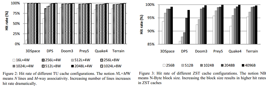
7 DESIGN SPACE EXPLORATION investigate the effects of changing the organization of the GPU caches on the hit rate (Streamer caches, Texture Unit caches, ZST caches and Color Write caches) The simulation results show negligible impact on the hit rate for all the caches, except for the TU and the ZST caches
8 TU CACHE The texture cache is a read-only cache that stores image data that is used for putting images onto triangles, a process called texture mapping. The texture cache has a high hit rate since there is heavy reuse between neighboring pixels temporal locality
9 ZST CACHE Z and Stencil Test caches take advantage of the spatial locality because of the very nature of the depth buffer where neighboring fragments are more likely to be fetched in an X-Y frame grid Depth buffer: When an object is rendered, the depth of a generated pixel (z coordinate) is stored in a buffer (the z-buffer or depth buffer). This buffer is usually arranged as a two-dimensional array (x-y) with one element for each screen pixel.
10
11 DESIGN SPACE EXPLORATION CONT D use the 3DCacti simulator in order to determine the extra cycles incurred due to size increase These 2-layer and 4-layer caches were die-stacked by dividing the word lines. increasing the cache size increases the latency; however, dividing the caches into a number of layers has reduced latency.
12 3D COST MODEL There are a number of techniques for stacking dies of which Wafer-to-Wafer (W2W) and Die-to-Wafer (D2W) techniques are the most common. Unlike W2W, D2W allows for stacking individual dies to another wafer resulting in higher flexibility and higher yield. Die Cost: Cost of fabricating a single die before 3D bonding Bonding Cost: Cost incurred due to bonding (We assume a bonding cost of $150 per wafer) Die Yield: The die area is inversely proportional to the die yield. Bonding Yield(Our 3D bonding cost model is based on the 3D process from our industry partners, with the assumption that the yield of each 3D process step is 99%.) Known-Good-Die testing cost
13 ISO-CYCLE TIME RESULTS Assume iso-cycle time is 0.75 ns. This cycle time captures typical frequency ranges used in current GPUs
14 SCENARIO I a 2D GPU vs a 3Dstacked cache GPU. Both GPUs contain 128 shaders, and both utilize 65nm technology. The first layer in the 3D GPU contains the GPU processing units, while the other two layers contain the partitioned ZST and TU caches 3D architecture achieves up to 45% speed up over the 2D planar architecture Total power: 106.4W Maximum temperature: ºC(hotspot simulation tool)
15 SCENARIO II: HETEROGENEOUS INTEGRATION In the first layer of the 3D design, we implement the GPU units in 65nm technology. However, the second layer uses 45nm technology Working with smaller feature sizes allows us to cram all the caches into one layer saving cost incurred due to bonding. 3D design outperformed 2D by a 19% geometric mean speedup. Total power: 82.1W Maximum temperature: 82.24ºC(hotspot simulation tool)
16 MRAM VS. SRAM Since leakage power(a gradual loss of energy from a charged capacitor) is an important component of power consumption, we consider the impact of utilizing non-volatile Magnetic Random Access Memory (MRAM) that has zero standby power as a candidate for implementing caches. leakage power: a gradual loss of energy from a charged capacitor Standby power: the electric power consumed by electronic and electrical appliances while they are switched off or in a standby mode.
17 MAGNETORESISTIVE RANDOM-ACCESS MEMORY (MRAM) Unlike conventional RAM chip technologies, data in MRAM is not stored as electric charge or current flows, but by magnetic storage elements. The heart of an MRAM memory cell is the magnetic tunnel junction (MTJ), a small device having two ferromagnetic layers separated by a thin dielectric layer as shown below: The resistance of the MTJ is low if they are parallel( 1 ) and high if they are antiparallel( 0 ). Not only does it retain its memory with the power turned off but also there is no constant power-draw. the write process is slower and requires more power to overcome the existing field stored in the junction.

18 MRAM VS. SRAM CONT D For caches with a less number of writes compared to reads, we observed a performance gain. However, due to the slow write times of the MRAM, compared to SRAM, when the number of writes is large, there is performance degradation.
19 MRAM VS. SRAM CONT D The power benefits of MRAM over SRAM makes the former more appealing for power-conserving applications.
20 CONTRIBUTIONS Performance evaluation of 3Dstacked caches on GPUs Comparison between 3D stacked SRAMs and MRAMs in GPUs in terms of power consumptions Power and thermal analysis of proposed architectural designs.
21 Questions?
1. Memory technology & Hierarchy
 1. Memory technology & Hierarchy RAM types Advances in Computer Architecture Andy D. Pimentel Memory wall Memory wall = divergence between CPU and RAM speed We can increase bandwidth by introducing concurrency
Photonic Networks for Data Centres and High Performance Computing
 Photonic Networks for Data Centres and High Performance Computing Philip Watts Department of Electronic Engineering, UCL Yury Audzevich, Nick Barrow-Williams, Robert Mullins, Simon Moore, Andrew Moore
State-of-the-Art Flash Memory Technology, Looking into the Future
 State-of-the-Art Flash Memory Technology, Looking into the Future April 16 th, 2012 大 島 成 夫 (Jeff Ohshima) Technology Executive Memory Design and Application Engineering Semiconductor and Storage Products
Computer Graphics Hardware An Overview
 Computer Graphics Hardware An Overview Graphics System Monitor Input devices CPU/Memory GPU Raster Graphics System Raster: An array of picture elements Based on raster-scan TV technology The screen (and
Low power GPUs a view from the industry. Edvard Sørgård
 Low power GPUs a view from the industry Edvard Sørgård 1 ARM in Trondheim Graphics technology design centre From 2006 acquisition of Falanx Microsystems AS Origin of the ARM Mali GPUs Main activities today
3D IC Design and CAD Challenges
 3D IC Design and CAD Challenges Ruchir Puri IBM T J Watson Research Center Yorktown Heights, NY 10598 Precedent for 3D Integration: When Real Estate Becomes Pricey 1900 Vertical Integration isn t new!
GPU Architecture. Michael Doggett ATI
 GPU Architecture Michael Doggett ATI GPU Architecture RADEON X1800/X1900 Microsoft s XBOX360 Xenos GPU GPU research areas ATI - Driving the Visual Experience Everywhere Products from cell phones to super
Embedded STT-MRAM for Mobile Applications:
 Embedded STT-MRAM for Mobile Applications: Enabling Advanced Chip Architectures Seung H. Kang Qualcomm Inc. Acknowledgments I appreciate valuable contributions and supports from Kangho Lee, Xiaochun Zhu,
State-of-Art (SoA) System-on-Chip (SoC) Design HPC SoC Workshop
 System-on-Chip (SoC) Design HPC SoC Workshop") Photos placed in horizontal position with even amount of white space between photos and header State-of-Art (SoA) System-on-Chip (SoC) Design HPC SoC Workshop Michael Holmes Manager, Mixed Signal ASIC/SoC
Photos placed in horizontal position with even amount of white space between photos and header State-of-Art (SoA) System-on-Chip (SoC) Design HPC SoC Workshop Michael Holmes Manager, Mixed Signal ASIC/SoC
With respect to the way of data access we can classify memories as:
 Memory Classification With respect to the way of data access we can classify memories as: - random access memories (RAM), - sequentially accessible memory (SAM), - direct access memory (DAM), - contents
From physics to products
 From physics to products From MRAM to MLU and beyond memory Magnetic Random Access Memory Magnetic Logic Unit Lucien Lombard Crocus-Technology Overview 1 - The semiconductor industry 2 - Crocus-Technology
361 Computer Architecture Lecture 14: Cache Memory
 1 361 Computer Architecture Lecture 14 Memory cache.1 The Motivation for s Memory System Processor DRAM Motivation Large memories (DRAM) are slow Small memories (SRAM) are fast Make the average access
NAND Flash FAQ. Eureka Technology. apn5_87. NAND Flash FAQ
 What is NAND Flash? What is the major difference between NAND Flash and other Memory? Structural differences between NAND Flash and NOR Flash What does NAND Flash controller do? How to send command to
COMPUTER HARDWARE. Input- Output and Communication Memory Systems
 COMPUTER HARDWARE Input- Output and Communication Memory Systems Computer I/O I/O devices commonly found in Computer systems Keyboards Displays Printers Magnetic Drives Compact disk read only memory (CD-ROM)
Module 2. Embedded Processors and Memory. Version 2 EE IIT, Kharagpur 1
 Module 2 Embedded Processors and Memory Version 2 EE IIT, Kharagpur 1 Lesson 5 Memory-I Version 2 EE IIT, Kharagpur 2 Instructional Objectives After going through this lesson the student would Pre-Requisite
Samsung emcp. WLI DDP Package. Samsung Multi-Chip Packages can help reduce the time to market for handheld devices BROCHURE
 Samsung emcp Samsung Multi-Chip Packages can help reduce the time to market for handheld devices WLI DDP Package Deliver innovative portable devices more quickly. Offer higher performance for a rapidly
GPU(Graphics Processing Unit) with a Focus on Nvidia GeForce 6 Series. By: Binesh Tuladhar Clay Smith
 with a Focus on Nvidia GeForce 6 Series. By: Binesh Tuladhar Clay Smith") GPU(Graphics Processing Unit) with a Focus on Nvidia GeForce 6 Series By: Binesh Tuladhar Clay Smith Overview History of GPU s GPU Definition Classical Graphics Pipeline Geforce 6 Series Architecture Vertex
GPU(Graphics Processing Unit) with a Focus on Nvidia GeForce 6 Series By: Binesh Tuladhar Clay Smith Overview History of GPU s GPU Definition Classical Graphics Pipeline Geforce 6 Series Architecture Vertex
Non-Volatile Memory. Non-Volatile Memory & its use in Enterprise Applications. Contents
 Non-Volatile Memory Non-Volatile Memory & its use in Enterprise Applications Author: Adrian Proctor, Viking Technology [email: adrian.proctor@vikingtechnology.com] This paper reviews different memory technologies,
Bi-directional FlipFET TM MOSFETs for Cell Phone Battery Protection Circuits
 Bi-directional FlipFET TM MOSFETs for Cell Phone Battery Protection Circuits As presented at PCIM 2001 Authors: *Mark Pavier, *Hazel Schofield, *Tim Sammon, **Aram Arzumanyan, **Ritu Sodhi, **Dan Kinzer
Alpha CPU and Clock Design Evolution
 Alpha CPU and Clock Design Evolution This lecture uses two papers that discuss the evolution of the Alpha CPU and clocking strategy over three CPU generations Gronowski, Paul E., et.al., High Performance
Intel s Revolutionary 22 nm Transistor Technology
 Intel s Revolutionary 22 nm Transistor Technology Mark Bohr Intel Senior Fellow Kaizad Mistry 22 nm Program Manager May, 2011 1 Key Messages Intel is introducing revolutionary Tri-Gate transistors on its
Why Hybrid Storage Strategies Give the Best Bang for the Buck
 JANUARY 28, 2014, SAN JOSE, CA Tom Coughlin, Coughlin Associates & Jim Handy, Objective Analysis PRESENTATION TITLE GOES HERE Why Hybrid Storage Strategies Give the Best Bang for the Buck 1 Outline Different
How to Optimize 3D CMP Cache Hierarchy
 3D Cache Hierarchy Optimization Leonid Yavits, Amir Morad, Ran Ginosar Department of Electrical Engineering Technion Israel Institute of Technology Haifa, Israel yavits@tx.technion.ac.il, amirm@tx.technion.ac.il,
In-Memory Databases Algorithms and Data Structures on Modern Hardware. Martin Faust David Schwalb Jens Krüger Jürgen Müller
 In-Memory Databases Algorithms and Data Structures on Modern Hardware Martin Faust David Schwalb Jens Krüger Jürgen Müller The Free Lunch Is Over 2 Number of transistors per CPU increases Clock frequency
Chapter 1 Computer System Overview
 Operating Systems: Internals and Design Principles Chapter 1 Computer System Overview Eighth Edition By William Stallings Operating System Exploits the hardware resources of one or more processors Provides
1.Introduction. Introduction. Most of slides come from Semiconductor Manufacturing Technology by Michael Quirk and Julian Serda.
 .Introduction If the automobile had followed the same development cycle as the computer, a Rolls- Royce would today cost $00, get one million miles to the gallon and explode once a year Most of slides
GPGPU Computing. Yong Cao
 GPGPU Computing Yong Cao Why Graphics Card? It s powerful! A quiet trend Copyright 2009 by Yong Cao Why Graphics Card? It s powerful! Processor Processing Units FLOPs per Unit Clock Speed Processing Power
1 / 25. CS 137: File Systems. Persistent Solid-State Storage
 1 / 25 CS 137: File Systems Persistent Solid-State Storage Technology Change is Coming Introduction Disks are cheaper than any solid-state memory Likely to be true for many years But SSDs are now cheap
Agenda. Michele Taliercio, Il circuito Integrato, Novembre 2001
 Agenda Introduzione Il mercato Dal circuito integrato al System on a Chip (SoC) La progettazione di un SoC La tecnologia Una fabbrica di circuiti integrati 28 How to handle complexity G The engineering
Samsung 2bit 3D V-NAND technology
 Samsung 2bit 3D V-NAND technology Gain more capacity, speed, endurance and power efficiency Traditional NAND technology cannot keep pace with growing data demands Introduction Data traffic continues to
MOSFET TECHNOLOGY ADVANCES DC-DC CONVERTER EFFICIENCY FOR PROCESSOR POWER
 MOSFET TECHNOLOGY ADVANCES DC-DC CONVERTER EFFICIENCY FOR PROCESSOR POWER Naresh Thapar, R.Sodhi, K.Dierberger, G.Stojcic, C.Blake, and D.Kinzer International Rectifier Corporation El Segundo, CA 90245.
Slide Set 8. for ENCM 369 Winter 2015 Lecture Section 01. Steve Norman, PhD, PEng
 Slide Set 8 for ENCM 369 Winter 2015 Lecture Section 01 Steve Norman, PhD, PEng Electrical & Computer Engineering Schulich School of Engineering University of Calgary Winter Term, 2015 ENCM 369 W15 Section
Aeroflex Solutions for Stacked Memory Packaging Increasing Density while Decreasing Area
 Aeroflex Solutions for Stacked Memory Packaging Increasing Density while Decreasing Area Authors: Ronald Lake Tim Meade, Sean Thorne, Clark Kenyon, Richard Jadomski www.aeroflex.com/memories Military and
Static-Noise-Margin Analysis of Conventional 6T SRAM Cell at 45nm Technology
 Static-Noise-Margin Analysis of Conventional 6T SRAM Cell at 45nm Technology Nahid Rahman Department of electronics and communication FET-MITS (Deemed university), Lakshmangarh, India B. P. Singh Department
The Quest for Speed - Memory. Cache Memory. A Solution: Memory Hierarchy. Memory Hierarchy
 The Quest for Speed - Memory Cache Memory CSE 4, Spring 25 Computer Systems http://www.cs.washington.edu/4 If all memory accesses (IF/lw/sw) accessed main memory, programs would run 20 times slower And
Load Balancing & DFS Primitives for Efficient Multicore Applications
 Load Balancing & DFS Primitives for Efficient Multicore Applications M. Grammatikakis, A. Papagrigoriou, P. Petrakis, G. Kornaros, I. Christophorakis TEI of Crete This work is implemented through the Operational
The Evolving NAND Flash Business Model for SSD. Steffen Hellmold VP BD, SandForce
 The Evolving NAND Flash Business Model for SSD Steffen Hellmold VP BD, SandForce Flash Forward: Flash Flash Memory Memory Storage Storage Solutions Solutions Solid State Storage - Vision Solid State Storage
Implementation of Buffer Cache Simulator for Hybrid Main Memory and Flash Memory Storages
 Implementation of Buffer Cache Simulator for Hybrid Main Memory and Flash Memory Storages Soohyun Yang and Yeonseung Ryu Department of Computer Engineering, Myongji University Yongin, Gyeonggi-do, Korea
Homework # 2. Solutions. 4.1 What are the differences among sequential access, direct access, and random access?
 ECE337 / CS341, Fall 2005 Introduction to Computer Architecture and Organization Instructor: Victor Manuel Murray Herrera Date assigned: 09/19/05, 05:00 PM Due back: 09/30/05, 8:00 AM Homework # 2 Solutions
Radeon HD 2900 and Geometry Generation. Michael Doggett
 Radeon HD 2900 and Geometry Generation Michael Doggett September 11, 2007 Overview Introduction to 3D Graphics Radeon 2900 Starting Point Requirements Top level Pipeline Blocks from top to bottom Command
Emerging storage and HPC technologies to accelerate big data analytics Jerome Gaysse JG Consulting
 Emerging storage and HPC technologies to accelerate big data analytics Jerome Gaysse JG Consulting Introduction Big Data Analytics needs: Low latency data access Fast computing Power efficiency Latest
Evaluating STT-RAM as an Energy-Efficient Main Memory Alternative
 1 Evaluating STT-RAM as an Energy-Efficient Main Memory Alternative Emre Kültürsay, Mahmut Kandemir, Anand Sivasubramaniam, and Onur Mutlu The Pennsylvania State University and Carnegie Mellon University
Computer Systems Structure Main Memory Organization
 Computer Systems Structure Main Memory Organization Peripherals Computer Central Processing Unit Main Memory Computer Systems Interconnection Communication lines Input Output Ward 1 Ward 2 Storage/Memory
Memory Basics. SRAM/DRAM Basics
 Memory Basics RAM: Random Access Memory historically defined as memory array with individual bit access refers to memory with both Read and Write capabilities ROM: Read Only Memory no capabilities for
Interconnection technologies
 Interconnection technologies Ron Ho VLSI Research Group Sun Microsystems Laboratories 1 Acknowledgements Many contributors to the work described here > Robert Drost, David Hopkins, Alex Chow, Tarik Ono,
Semiconductor Memories
 Semiconductor Memories Semiconductor memories array capable of storing large quantities of digital information are essential to all digital systems Maximum realizable data storage capacity of a single
Parallel Simplification of Large Meshes on PC Clusters
 Parallel Simplification of Large Meshes on PC Clusters Hua Xiong, Xiaohong Jiang, Yaping Zhang, Jiaoying Shi State Key Lab of CAD&CG, College of Computer Science Zhejiang University Hangzhou, China April
Low Power AMD Athlon 64 and AMD Opteron Processors
 Low Power AMD Athlon 64 and AMD Opteron Processors Hot Chips 2004 Presenter: Marius Evers Block Diagram of AMD Athlon 64 and AMD Opteron Based on AMD s 8 th generation architecture AMD Athlon 64 and AMD
Memory Architecture and Management in a NoC Platform
 Architecture and Management in a NoC Platform Axel Jantsch Xiaowen Chen Zhonghai Lu Chaochao Feng Abdul Nameed Yuang Zhang Ahmed Hemani DATE 2011 Overview Motivation State of the Art Data Management Engine
Samsung 3bit 3D V-NAND technology
 White Paper Samsung 3bit 3D V-NAND technology Yield more capacity, performance and power efficiency Stay abreast of increasing data demands with Samsung's innovative vertical architecture Introduction
Architectures and Platforms
 Hardware/Software Codesign Arch&Platf. - 1 Architectures and Platforms 1. Architecture Selection: The Basic Trade-Offs 2. General Purpose vs. Application-Specific Processors 3. Processor Specialisation
Graphics Cards and Graphics Processing Units. Ben Johnstone Russ Martin November 15, 2011
 Graphics Cards and Graphics Processing Units Ben Johnstone Russ Martin November 15, 2011 Contents Graphics Processing Units (GPUs) Graphics Pipeline Architectures 8800-GTX200 Fermi Cayman Performance Analysis
Computer Architecture
 Computer Architecture Random Access Memory Technologies 2015. április 2. Budapest Gábor Horváth associate professor BUTE Dept. Of Networked Systems and Services ghorvath@hit.bme.hu 2 Storing data Possible
Touchstone -A Fresh Approach to Multimedia for the PC
 Touchstone -A Fresh Approach to Multimedia for the PC Emmett Kilgariff Martin Randall Silicon Engineering, Inc Presentation Outline Touchstone Background Chipset Overview Sprite Chip Tiler Chip Compressed
Flash Memories. João Pela (52270), João Santos (55295) December 22, 2008 IST
, João Santos (55295) December 22, 2008 IST") Flash Memories João Pela (52270), João Santos (55295) IST December 22, 2008 João Pela (52270), João Santos (55295) (IST) Flash Memories December 22, 2008 1 / 41 Layout 1 Introduction 2 How they work 3
Flash Memories João Pela (52270), João Santos (55295) IST December 22, 2008 João Pela (52270), João Santos (55295) (IST) Flash Memories December 22, 2008 1 / 41 Layout 1 Introduction 2 How they work 3
Analyzing Electrical Effects of RTA-driven Local Anneal Temperature Variation
 1 Analyzing Electrical Effects of RTA-driven Local Anneal Temperature Variation Vivek Joshi, Kanak Agarwal*, Dennis Sylvester, David Blaauw Electrical Engineering & Computer Science University of Michigan,
Yaffs NAND Flash Failure Mitigation
 Yaffs NAND Flash Failure Mitigation Charles Manning 2012-03-07 NAND flash is one of very few types of electronic device which are knowingly shipped with errors and are expected to generate further errors
Efficient Interconnect Design with Novel Repeater Insertion for Low Power Applications
 Efficient Interconnect Design with Novel Repeater Insertion for Low Power Applications TRIPTI SHARMA, K. G. SHARMA, B. P. SINGH, NEHA ARORA Electronics & Communication Department MITS Deemed University,
Computer Systems Structure Input/Output
 Computer Systems Structure Input/Output Peripherals Computer Central Processing Unit Main Memory Computer Systems Interconnection Communication lines Input Output Ward 1 Ward 2 Examples of I/O Devices
Architectures and Design Methodologies for Micro and Nanocomputing
 Architectures and Design Methodologies for Micro and Nanocomputing PhD Poster Day, December 4, 2014 Matteo Bollo 1 (ID: 24367, I PhD Year) Tutor: Maurizio Zamboni 1 Collaborators: Mariagrazia Graziano
Writing Applications for the GPU Using the RapidMind Development Platform
 Writing Applications for the GPU Using the RapidMind Development Platform Contents Introduction... 1 Graphics Processing Units... 1 RapidMind Development Platform... 2 Writing RapidMind Enabled Applications...
L20: GPU Architecture and Models
 L20: GPU Architecture and Models scribe(s): Abdul Khalifa 20.1 Overview GPUs (Graphics Processing Units) are large parallel structure of processing cores capable of rendering graphics efficiently on displays.
Flash & DRAM Si Scaling Challenges, Emerging Non-Volatile Memory Technology Enablement - Implications to Enterprise Storage and Server Compute systems
 Flash & DRAM Si Scaling Challenges, Emerging Non-Volatile Memory Technology Enablement - Implications to Enterprise Storage and Server Compute systems Jung H. Yoon, Hillery C. Hunter, Gary A. Tressler
Memory. The memory types currently in common usage are:
 ory ory is the third key component of a microprocessor-based system (besides the CPU and I/O devices). More specifically, the primary storage directly addressed by the CPU is referred to as main memory
On-Chip Interconnection Networks Low-Power Interconnect
 On-Chip Interconnection Networks Low-Power Interconnect William J. Dally Computer Systems Laboratory Stanford University ISLPED August 27, 2007 ISLPED: 1 Aug 27, 2007 Outline Demand for On-Chip Networks
Implementation Of High-k/Metal Gates In High-Volume Manufacturing
 White Paper Implementation Of High-k/Metal Gates In High-Volume Manufacturing INTRODUCTION There have been significant breakthroughs in IC technology in the past decade. The upper interconnect layers of
White Paper: Pervasive Power: Integrated Energy Storage for POL Delivery
 Pervasive Power: Integrated Energy Storage for POL Delivery Pervasive Power Overview This paper introduces several new concepts for micro-power electronic system design. These concepts are based on the
CHAPTER 7: The CPU and Memory
 CHAPTER 7: The CPU and Memory The Architecture of Computer Hardware, Systems Software & Networking: An Information Technology Approach 4th Edition, Irv Englander John Wiley and Sons 2010 PowerPoint slides
Chapter 2: Computer-System Structures. Computer System Operation Storage Structure Storage Hierarchy Hardware Protection General System Architecture
 Chapter 2: Computer-System Structures Computer System Operation Storage Structure Storage Hierarchy Hardware Protection General System Architecture Operating System Concepts 2.1 Computer-System Architecture
ADVANCED PROCESSOR ARCHITECTURES AND MEMORY ORGANISATION Lesson-17: Memory organisation, and types of memory
 ADVANCED PROCESSOR ARCHITECTURES AND MEMORY ORGANISATION Lesson-17: Memory organisation, and types of memory 1 1. Memory Organisation 2 Random access model A memory-, a data byte, or a word, or a double
From Bus and Crossbar to Network-On-Chip. Arteris S.A.
 From Bus and Crossbar to Network-On-Chip Arteris S.A. Copyright 2009 Arteris S.A. All rights reserved. Contact information Corporate Headquarters Arteris, Inc. 1741 Technology Drive, Suite 250 San Jose,
Wafer Level Testing Challenges for Flip Chip and Wafer Level Packages
 Wafer Level Testing Challenges for Flip Chip and Wafer Level Packages by Lim Kok Hwa and Andy Chee STATS ChipPAC Ltd. 5 Yishun Street 23, Singapore 768442 kokhwa.lim@statschippac.com; kenghwee.chee@statschippac.com
Introduction to Digital System Design
 Introduction to Digital System Design Chapter 1 1 Outline 1. Why Digital? 2. Device Technologies 3. System Representation 4. Abstraction 5. Development Tasks 6. Development Flow Chapter 1 2 1. Why Digital
Lecture 11: Multi-Core and GPU. Multithreading. Integration of multiple processor cores on a single chip.
 Lecture 11: Multi-Core and GPU Multi-core computers Multithreading GPUs General Purpose GPUs Zebo Peng, IDA, LiTH 1 Multi-Core System Integration of multiple processor cores on a single chip. To provide
AN1837. Non-Volatile Memory Technology Overview By Stephen Ledford Non-Volatile Memory Technology Center Austin, Texas.
 Order this document by /D Non-Volatile Memory Technology Overview By Stephen Ledford Non-Volatile Memory Technology Center Austin, Texas Introduction Today s microcontroller applications are more sophisticated
Non-Volatile Memory and Its Use in Enterprise Applications
 Non-Volatile Memory and Its Use in Enterprise Applications Contributor: Viking Technology January 2014 About the SNIA The Storage Networking Industry Association (SNIA) is a not for profit global organization,
Thermal Modeling Methodology for Fast and Accurate System-Level Analysis: Application to a Memory-on-Logic 3D Circuit
 Thermal Modeling Methodology for Fast and Accurate System-Level Analysis: Application to a Memory-on-Logic 3D Circuit Cristiano Santos 1,2, Pascal Vivet 1, Philippe Garrault 3, Nicolas Peltier 3, Sylvian
AMD Opteron Quad-Core
 AMD Opteron Quad-Core a brief overview Daniele Magliozzi Politecnico di Milano Opteron Memory Architecture native quad-core design (four cores on a single die for more efficient data sharing) enhanced
Computer Architecture-I
 Computer Architecture-I 1. Die Yield is given by the formula, Assignment 1 Solution Die Yield = Wafer Yield x (1 + (Defects per unit area x Die Area)/a) -a Let us assume a wafer yield of 100% and a 4 for
Design Compiler Graphical Create a Better Starting Point for Faster Physical Implementation
 Datasheet Create a Better Starting Point for Faster Physical Implementation Overview Continuing the trend of delivering innovative synthesis technology, Design Compiler Graphical delivers superior quality
what operations can it perform? how does it perform them? on what kind of data? where are instructions and data stored?
 Inside the CPU how does the CPU work? what operations can it perform? how does it perform them? on what kind of data? where are instructions and data stored? some short, boring programs to illustrate the
Hyper Node Torus: A New Interconnection Network for High Speed Packet Processors
 2011 International Symposium on Computer Networks and Distributed Systems (CNDS), February 23-24, 2011 Hyper Node Torus: A New Interconnection Network for High Speed Packet Processors Atefeh Khosravi,
Dry Film Photoresist & Material Solutions for 3D/TSV
 Dry Film Photoresist & Material Solutions for 3D/TSV Agenda Digital Consumer Market Trends Components and Devices 3D Integration Approaches Examples of TSV Applications Image Sensor and Memory Via Last
2014 EMERGING NON- VOLATILE MEMORY & STORAGE TECHNOLOGIES AND MANUFACTURING REPORT
 2014 EMERGING NON- VOLATILE MEMORY & STORAGE TECHNOLOGIES AND MANUFACTURING REPORT COUGHLIN ASSOCIATES SAN JOSE, CALIFORNIA April 2014 2014 Emerging NV Memory & Storage Technologies and Manufacturing Report
Lecture 030 DSM CMOS Technology (3/24/10) Page 030-1
 Page 030-1") Lecture 030 DSM CMOS Technology (3/24/10) Page 030-1 LECTURE 030 - DEEP SUBMICRON (DSM) CMOS TECHNOLOGY LECTURE ORGANIZATION Outline Characteristics of a deep submicron CMOS technology Typical deep submicron
Lecture 030 DSM CMOS Technology (3/24/10) Page 030-1 LECTURE 030 - DEEP SUBMICRON (DSM) CMOS TECHNOLOGY LECTURE ORGANIZATION Outline Characteristics of a deep submicron CMOS technology Typical deep submicron
Note monitors controlled by analog signals CRT monitors are controlled by analog voltage. i. e. the level of analog signal delivered through the
 DVI Interface The outline: The reasons for digital interface of a monitor the transfer from VGA to DVI. DVI v. analog interface. The principles of LCD control through DVI interface. The link between DVI
Programming NAND devices
 Technical Guide Programming NAND devices Kelly Hirsch, Director of Advanced Technology, Data I/O Corporation Recent Design Trends In the past, embedded system designs have used NAND devices for storing
Energy-Efficient, High-Performance Heterogeneous Core Design
 Energy-Efficient, High-Performance Heterogeneous Core Design Raj Parihar Core Design Session, MICRO - 2012 Advanced Computer Architecture Lab, UofR, Rochester April 18, 2013 Raj Parihar Energy-Efficient,
Advancements in High Frequency, High Resolution Acoustic Micro Imaging for Thin Silicon Applications
 Advancements in High Frequency, High Resolution Acoustic Micro Imaging for Thin Silicon Applications Janet E. Semmens Sonoscan, Inc. 2149 E. Pratt Boulevard Elk Grove Village, IL 60007 USA Phone: (847)
Price/performance Modern Memory Hierarchy
 Lecture 21: Storage Administration Take QUIZ 15 over P&H 6.1-4, 6.8-9 before 11:59pm today Project: Cache Simulator, Due April 29, 2010 NEW OFFICE HOUR TIME: Tuesday 1-2, McKinley Last Time Exam discussion
Solid State Drive Architecture
 Solid State Drive Architecture A comparison and evaluation of data storage mediums Tyler Thierolf Justin Uriarte Outline Introduction Storage Device as Limiting Factor Terminology Internals Interface Architecture
Lecture 18: Interconnection Networks. CMU 15-418: Parallel Computer Architecture and Programming (Spring 2012)
") Lecture 18: Interconnection Networks CMU 15-418: Parallel Computer Architecture and Programming (Spring 2012) Announcements Project deadlines: - Mon, April 2: project proposal: 1-2 page writeup - Fri,
Lecture 18: Interconnection Networks CMU 15-418: Parallel Computer Architecture and Programming (Spring 2012) Announcements Project deadlines: - Mon, April 2: project proposal: 1-2 page writeup - Fri,
Switch Fabric Implementation Using Shared Memory
 Order this document by /D Switch Fabric Implementation Using Shared Memory Prepared by: Lakshmi Mandyam and B. Kinney INTRODUCTION Whether it be for the World Wide Web or for an intra office network, today
Nanotechnologies for the Integrated Circuits
 Nanotechnologies for the Integrated Circuits September 23, 2015 Dr. Bertrand Cambou Professor of Practice NAU, Cybersecurity School of Informatics, Computing, and Cyber-Systems Agenda The Market Silicon
Power Analysis of Link Level and End-to-end Protection in Networks on Chip
 Power Analysis of Link Level and End-to-end Protection in Networks on Chip Axel Jantsch, Robert Lauter, Arseni Vitkowski Royal Institute of Technology, tockholm May 2005 ICA 2005 1 ICA 2005 2 Overview
Understanding LCD Memory and Bus Bandwidth Requirements ColdFire, LCD, and Crossbar Switch
 Freescale Semiconductor Application Note Document Number: AN3606 Rev. 0, 03/2008 Understanding LCD Memory and Bus Bandwidth Requirements ColdFire, LCD, and Crossbar Switch by: Melissa Hunter TSPG Applications
Parallel Programming Survey
 Christian Terboven 02.09.2014 / Aachen, Germany Stand: 26.08.2014 Version 2.3 IT Center der RWTH Aachen University Agenda Overview: Processor Microarchitecture Shared-Memory
The continuum of data management techniques for explicitly managed systems
 The continuum of data management techniques for explicitly managed systems Svetozar Miucin, Craig Mustard Simon Fraser University MCES 2013. Montreal Introduction Explicitly Managed Memory systems lack
How To Teach Computer Graphics
 Computer Graphics Thilo Kielmann Lecture 1: 1 Introduction (basic administrative information) Course Overview + Examples (a.o. Pixar, Blender, ) Graphics Systems Hands-on Session General Introduction http://www.cs.vu.nl/~graphics/
Real-Time Realistic Rendering. Michael Doggett Docent Department of Computer Science Lund university
 Real-Time Realistic Rendering Michael Doggett Docent Department of Computer Science Lund university 30-5-2011 Visually realistic goal force[d] us to completely rethink the entire rendering process. Cook