Memory. Memory structures are critical to any large, complex digital design.
|
|
|
- Ashlee Farmer
- 7 years ago
- Views:
Transcription
1 Memory

2 Memory Memory structures are critical to any large, complex digital design. 2

3 Memory Memory structures are crucial in digital design. ROM, PROM, EPROM, RAM, SRAM, (S)DRAM, RDRAM,.. All memory structures have an address bus and a data bus Possibly other control signals to control output etc. E.g. 4 Bit Address bus with 5 Bit Data Bus 2 4 x 5 ROM/RAM ADDR<3:0> DOUT<4:0> 3

4 Memory Internal organisation Lookup Table of values For each address there is a corresponding data output 16 possible address values with 5 bit output (16 x 5 ROM) ADDR<3:0> ADDR DOUT<4:0> DOUT

5 Memory Usually consider a repository for data or program code. Indexing of the data and ability to both read and write suggests a mailslot analogy. Byte = 8 bits Word = whatever data width you re using But, especially when considering read only, Lookup Table Truth Table ADDR DOUT

6 ROM k-input, n-output Read Only Memory (ROM) could be 2 k x n element lookup table k-input, n-output truth table k-input, n-output combinatorial logic block DOUT(0) = ADDR(3).ADDR(2).ADDR(1).ADDR(0) + ADDR(3).ADDR(2).. Any k-input, n-output combinatorial block is available Benefits Configure once PCB complete Flatten complex logic hierarchy to faster design Simple to create using high level language - no minimisation. 6

7 ROM - VHDL VHDL Code Various forms of coding possible E.g. if addr = 0000 then Or case addr is, when 0000 => (better) A neater approach is to use a table of constants See next slide! Could also easily add in further control signals etc. 7

8 ROM - VHDL use ieee.numeric_std.all; architecture BEHAVIOR of ROM is type romtable is array (0 to 15) of std_logic_vector(4 downto 0); constant romdata : romtable := ( 10101, 11111, etc.) ); begin process (ADDR) begin DOUT <= ROMDATA (to_integer(unsigned(addr))); end process; end BEHAVIOR; 8

9 ROM - VHDL Result after synthesis is simply a combinatorial logic implementation of the ROM i.e. DOUT(0) = ADDR(0) + ADDR(1) In practical terms, memory structures can be implemented on Silicon much more efficiently by use of technology specific implementation E.g. I need a 16 x 4 ROM with the values. As noted above - use high level language to calculate the values. For simulation/ small structures the above approach is feasible! 9

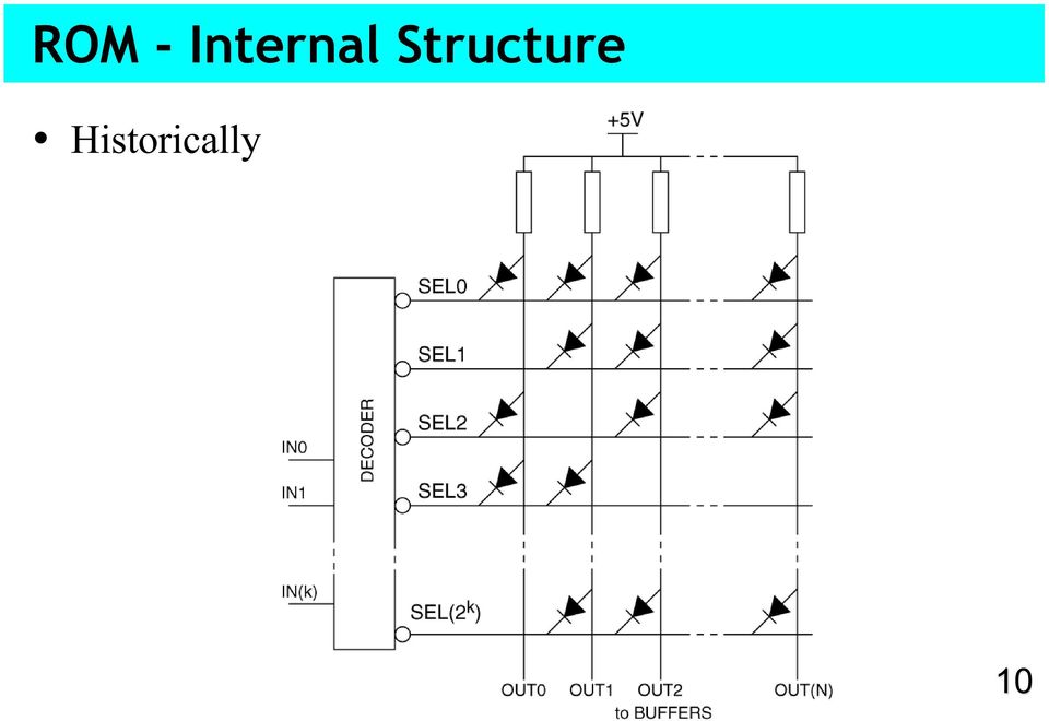
10 ROM - Internal Structure Historically 10
11 ROM - Internal Structure Why not just wires? 11

12 ROM - Internal Structure Modern structure. 12

13 ROM - Internal Structure The problem of decoding A k-input ROM requires a k-to-2 k decoder Such a decoder requires 2 k, k-input NAND gates, k buffers and k inverters, each with fanout of 2 k-1. 1Mbyte memory would obviously require over 1 million 20 input NAND gates, and 40 buffers/inverters with fanout of half a million, or a long (delay ridden) buffer chain. Ugh. And just how does such a beast fit into the system timing. Answer these questions when dealing with RAM. 13
 buffer chain. Ugh. And just how does such a beast fit into the system timing.")
14 Types of ROM - mask ROM Connections between word and bit lines are made by altering one or more interconnect masks in the fabrication process. 14

15 Types of ROM - mask ROM -2 Ideal for high volume, low cost production. Turn around on mask production and NRE (non recurring engineering) costs make them pointless for prototyping. 15
 costs make them")
16 Types of ROM - PROM Connections between word and bit lines destroyed by vaporising fusible links. Bipolar transistors typically used in these devices, so relatively high power, but fast nothing much faster than a wire in a microelectronic circuit! OTP (one time programmable) - obviously. Cheaper than EPROM or EEPROM and so often used in short production runs, or where the contents of the ROM may be altered right up to product launch but then set in stone. 16

17 Types of ROM - PROM - 2 Technology can be employed in the look up tables / fuse maps of OTP PLDs or, more rarely FPGAs. 17

18 Types of ROM - EPROM EPROM: Erasable, Programmable, Read Only Memory EEPROM: Electrically Erasable, Programmable, Read Only Memory flash EEPROM: a hybrid of the two. typically today EEPROM and flash EEPROM are both applied to flash EEPROM technology. 18

19 Types of ROM - EPROM - 2 Non volatile - 70% of charge remains after 10 years 19

20 Types of ROM - EPROM - 3 Device EPROM EEPROM flash EEPROM Channel-Floating 100 nm 10 nm 10 nm Gate Programme Avalanche Breakdown Fowler-Nordheim tunnelling Avalanche Breakdown Programming Time micro s milli s micro s Erasure UV light Fowler-Nordheim tunnelling Fowler-Nordheim tunnelling Erasure Time kilo s milli s / wordmilli s / word Programme/Erasure Cycles

21 E/EPROM Applications Firmware for embedded systems Microcontrollers - staggeringly huge market modems, graphics cards, etc. Embedded OS software for palmtops, set-top boxes, Bootstrap loaders Relatively cheap to produce. As markets expand, economies of scale make cheaper. OTP devices are now usually EPROMs without quartz lids. 21
22 E/EPROM Applications - 2 Technology is often employed in look up tables / fuse maps of PLDs or FPGAs Both PROMs and EEPROMs are readily available from 16 kbyte to 8 Mbyte configurations. Multiple flash EEPROMs can be packaged into flash card solid state memories. Can lever 40 mp3 encoded CD tracks into the largest sold today. 22
23 Random Access Memory Static, Dynamic, Synchronous and Asynchronous
24 RAM - Overview RAM (random access memory) read and write to any location given a valid address Historically term had more meaning when tape drives and punched cards were used for mass storage. Today hard disks are almost random, and modern RAM is not completely random. 24
25 RAM - Overview SRAM (static) Formed from internal latches - 6 transistors per bit. Latch will store information as long as power supplied. Inherently synchronous. Integrable. Fast, 12 ns access time direct from Farnell Fast, 4 ns access time in ECL from Cypress On chip caches, off chip caches, HD caches, 25
26 RAM - Overview DRAM (dynamic) Storage of charge on a capacitor gated by a transistor 1 ish transistor per bit. High packing density, large cheap memory, Cheap + economies of scale = very cheap. Commodity item. Less integrable Seriously faster than hard disk, 70 ns direct from Farnell Main memory These days most DRAM is also synchronous SDRAM 26
27 RAM - Overview SDRAM today PC100, k=64, 64 bit datapath at 100MHz How many bytes per second throughput / bandwidth? How many ns per clock cycle at 100MHz? Didn t we just say it took 70 ns to supply a byte from Farnell? PC133, k=64, 64 bit datapath at 133MHz How many bytes per second throughput / bandwidth? 27
28 RAM - Trends RDRAM (Rambus DRAM) PC600, k=16, at 266MHz, clocked on each edge! PC800, k=16, at 400MHz, clocked on each edge! Bandwidths? History Nintendo 64, Intel i820 chipset (bleugh), Playstation 2, not the Nintendo Dolphin, and practically no-one else. 28
29 RAM - Trends RDRAM Benefits But Fewer pins, so smaller PCB Internal guts does good look-ahead for streamed memory access. Proprietary ($$) However more difficult initial design due to high speed Streamed memory access random access memory Big heatsinks (not really built for your pretty Mac Cube) 29
30 RAM - Trends DDRDRAM (Double data rate DRAM) PC1600, k=64, at 100MHz, clocked on each edge! PC2100, k=64, at 133MHz, clocked on each edge! Benefits Cheaper Lower power consumption Better for truly random access (but not streamed) Already used in graphics cards AMD and almost everyone else apart from Intel. 30
31 RAM - interface Unless specifically designed (dual port), memory cannot be read from and written to at the same time. Instead of read and write, use r/^w (or write enable) and chip select signals. 31
32 Where are we? VHDL VHDL Combinatorial logic Counters, registers, state machines Memory ROM, SRAM, DRAM Arithmetic Logic Unit (ALU) Datapaths Sequencing and Control 32
33 async SRAM - internal structure Single SRAM cell BUG!! 33
34 async SRAM - internal structure 34
35 async SRAM The wrong way 35
36 async SRAM
37 RAM - timing Read process Choose desired word by applying address Ensure r/^w high Push chip select high and wait for a clock edge Read timing (CY7C102A, 256K 4 Static RAM) t AA, Address to valid data (12ns max) t OHA, Data hold from address change (3 ns min) t ACS, chip select to data valid (12 ns max) t CSLZ, chip select to low impedance (3 ns min) t CSHZ, chip select to high impedance (6 ns max) 37
38 RAM - timing 38
39 RAM - timing Write process Choose desired word slot by applying address to address lines Push r/^w low Push chip select low and apply data before it s raised high again. Write timing (CY7C102A) t AS, address set to write start (0 ns min) t CSW, chip enable pulse length (10 ns min) t DS, data setup to wite end (7 ns min) t DH, data hold to write end (0 ns min) all this assuming CS controlled write 39
40 RAM - timing 40
41 RAM - timing Read process similar to ROMs Latches - from schematic obviously no clock But aren t all our devices supposed to be synchronous? Edge triggered flip-flops would double silicon area Designers just accept the hassle in real systems. 41
42 synchronous SRAM - collaring/glue 42
43 sync SRAM Follow the same line as Wakerly Digital Design Principles and Practices - revise from 10.3 Chapter 6 of Mano & Kine Logic and Computer Design Fundamentals is fine as well. 43
44 sync SRAM - read operations 44
45 sync SRAM - write operations Problem? 45
46 sync SRAM - write operations Address delays are naturally longer than data delays. Need to add delay sections to keep the timing correct. Perfectly possible to do but in most memory systems not needed - two stage operation is usually helpful for the rest of the system. 46
47 sync SRAM - write operations Another problem! Need two cycles per memory access 47
48 sync SRAM - write operations 48
49 sync SRAM - write operations? 49
50 sync SRAM - write operations 50
51 sync SRAM - write operations ZBT SRAM (zero burst turnaround) shows an alternate method of solving the problem of the address needing to hang around for two clock cycles. Store it in another register Downside, waste of floorplan area.. Upside, can pipeline writes or interleave reads and writes. Wakerly - p865 Is it worth it? IBM POWER architecture. 51
52 sync SRAM - 1M x 8 bits How do we link multiple memories together? 52
53 sync SRAM - 1M x 16 bits 53
54 sync SRAM - 4M x 8 bits 54
55 DRAM Memory element is entirely different in detail Destructive Read Leakage Need for analogue row latch circuitry to amplify sense signal and feedback refresh. 55
56 DRAM - overall structure P.S. No Clock! 56
57 DRAM - read cycle Address to row address register put row data into row latch Recycle row latch back to row Pull out bit from row and send to output 57
58 DRAM - write cycle Address to row address register put row data into row latch Supply data bit and enable writing Read bit and refresh 58
59 DRAM - refresh cycle Address to row address register put row data into row latch Recycle row latch back to row 59
60 DRAM - refresh cycle 4Mx4bit DRAM requires each bit to be refreshed at least every 64 ms 4096 rows (1024 columns) so 4096 refreshes in 64 ms Available time therefore µs Actual refresh time is 60 ns per row. Less than 1%, so negligible if distributed 60
61 DRAM - refresh cycle Refresh cycle shown needs an external DRAM controller to step through the rows and supply refresh signals at appropriate times More modern method is CAS before RAS refresh (memory uses the otherwise unused CAS before RAS input to initiate a refresh cycle) which is associated with an internal refresh address counter. DRAM controller only chooses refresh times. 61
62 DRAM - other types EDO DRAM Still used in older machines Instead of output tri-state being controlled by CAS line becoming active on read cycle, an output enable signal is used. CAS still controls output timing, OE controls output tri-state Burst mode reads can happen much more quickly as no Z state between each one (extended data out) SDRAM Discussed before, collar some DRAM with synchronisers as in SRAM above, and then play pipelining tricks internally. 62
A N. O N Output/Input-output connection
 Memory Types Two basic types: ROM: Read-only memory RAM: Read-Write memory Four commonly used memories: ROM Flash, EEPROM Static RAM (SRAM) Dynamic RAM (DRAM), SDRAM, RAMBUS, DDR RAM Generic pin configuration:
Memory Basics. SRAM/DRAM Basics
 Memory Basics RAM: Random Access Memory historically defined as memory array with individual bit access refers to memory with both Read and Write capabilities ROM: Read Only Memory no capabilities for
Module 2. Embedded Processors and Memory. Version 2 EE IIT, Kharagpur 1
 Module 2 Embedded Processors and Memory Version 2 EE IIT, Kharagpur 1 Lesson 5 Memory-I Version 2 EE IIT, Kharagpur 2 Instructional Objectives After going through this lesson the student would Pre-Requisite
Memory. The memory types currently in common usage are:
 ory ory is the third key component of a microprocessor-based system (besides the CPU and I/O devices). More specifically, the primary storage directly addressed by the CPU is referred to as main memory
1. Memory technology & Hierarchy
 1. Memory technology & Hierarchy RAM types Advances in Computer Architecture Andy D. Pimentel Memory wall Memory wall = divergence between CPU and RAM speed We can increase bandwidth by introducing concurrency
Computer Architecture
 Computer Architecture Random Access Memory Technologies 2015. április 2. Budapest Gábor Horváth associate professor BUTE Dept. Of Networked Systems and Services ghorvath@hit.bme.hu 2 Storing data Possible
RAM & ROM Based Digital Design. ECE 152A Winter 2012
 RAM & ROM Based Digital Design ECE 152A Winter 212 Reading Assignment Brown and Vranesic 1 Digital System Design 1.1 Building Block Circuits 1.1.3 Static Random Access Memory (SRAM) 1.1.4 SRAM Blocks in
ADVANCED PROCESSOR ARCHITECTURES AND MEMORY ORGANISATION Lesson-17: Memory organisation, and types of memory
 ADVANCED PROCESSOR ARCHITECTURES AND MEMORY ORGANISATION Lesson-17: Memory organisation, and types of memory 1 1. Memory Organisation 2 Random access model A memory-, a data byte, or a word, or a double
Homework # 2. Solutions. 4.1 What are the differences among sequential access, direct access, and random access?
 ECE337 / CS341, Fall 2005 Introduction to Computer Architecture and Organization Instructor: Victor Manuel Murray Herrera Date assigned: 09/19/05, 05:00 PM Due back: 09/30/05, 8:00 AM Homework # 2 Solutions
Chapter 5 :: Memory and Logic Arrays
 Chapter 5 :: Memory and Logic Arrays Digital Design and Computer Architecture David Money Harris and Sarah L. Harris Copyright 2007 Elsevier 5- ROM Storage Copyright 2007 Elsevier 5- ROM Logic Data
Chapter 7 Memory and Programmable Logic
 NCNU_2013_DD_7_1 Chapter 7 Memory and Programmable Logic 71I 7.1 Introduction ti 7.2 Random Access Memory 7.3 Memory Decoding 7.5 Read Only Memory 7.6 Programmable Logic Array 77P 7.7 Programmable Array
Memory unit. 2 k words. n bits per word
 9- k address lines Read n data input lines Memory unit 2 k words n bits per word n data output lines 24 Pearson Education, Inc M Morris Mano & Charles R Kime 9-2 Memory address Binary Decimal Memory contents
Handout 17. by Dr Sheikh Sharif Iqbal. Memory Unit and Read Only Memories
 Handout 17 by Dr Sheikh Sharif Iqbal Memory Unit and Read Only Memories Objective: - To discuss different types of memories used in 80x86 systems for storing digital information. - To learn the electronic
Modeling Sequential Elements with Verilog. Prof. Chien-Nan Liu TEL: 03-4227151 ext:34534 Email: jimmy@ee.ncu.edu.tw. Sequential Circuit
 Modeling Sequential Elements with Verilog Prof. Chien-Nan Liu TEL: 03-4227151 ext:34534 Email: jimmy@ee.ncu.edu.tw 4-1 Sequential Circuit Outputs are functions of inputs and present states of storage elements
With respect to the way of data access we can classify memories as:
 Memory Classification With respect to the way of data access we can classify memories as: - random access memories (RAM), - sequentially accessible memory (SAM), - direct access memory (DAM), - contents
Computer Systems Structure Main Memory Organization
 Computer Systems Structure Main Memory Organization Peripherals Computer Central Processing Unit Main Memory Computer Systems Interconnection Communication lines Input Output Ward 1 Ward 2 Storage/Memory
SOLVING HIGH-SPEED MEMORY INTERFACE CHALLENGES WITH LOW-COST FPGAS
 SOLVING HIGH-SPEED MEMORY INTERFACE CHALLENGES WITH LOW-COST FPGAS A Lattice Semiconductor White Paper May 2005 Lattice Semiconductor 5555 Northeast Moore Ct. Hillsboro, Oregon 97124 USA Telephone: (503)
Computer Architecture
 Computer Architecture Slide Sets WS 2013/2014 Prof. Dr. Uwe Brinkschulte M.Sc. Benjamin Betting Part 11 Memory Management Computer Architecture Part 11 page 1 of 44 Prof. Dr. Uwe Brinkschulte, M.Sc. Benjamin
Computer Performance. Topic 3. Contents. Prerequisite knowledge Before studying this topic you should be able to:
 55 Topic 3 Computer Performance Contents 3.1 Introduction...................................... 56 3.2 Measuring performance............................... 56 3.2.1 Clock Speed.................................
GETTING STARTED WITH PROGRAMMABLE LOGIC DEVICES, THE 16V8 AND 20V8
 GETTING STARTED WITH PROGRAMMABLE LOGIC DEVICES, THE 16V8 AND 20V8 Robert G. Brown All Rights Reserved August 25, 2000 Alta Engineering 58 Cedar Lane New Hartford, CT 06057-2905 (860) 489-8003 www.alta-engineering.com
Technical Note. Micron NAND Flash Controller via Xilinx Spartan -3 FPGA. Overview. TN-29-06: NAND Flash Controller on Spartan-3 Overview
 Technical Note TN-29-06: NAND Flash Controller on Spartan-3 Overview Micron NAND Flash Controller via Xilinx Spartan -3 FPGA Overview As mobile product capabilities continue to expand, so does the demand
The Central Processing Unit:
 The Central Processing Unit: What Goes on Inside the Computer Chapter 4 Objectives Identify the components of the central processing unit and how they work together and interact with memory Describe how
Chapter 6. Inside the System Unit. What You Will Learn... Computers Are Your Future. What You Will Learn... Describing Hardware Performance
 What You Will Learn... Computers Are Your Future Chapter 6 Understand how computers represent data Understand the measurements used to describe data transfer rates and data storage capacity List the components
Introduction to Programmable Logic Devices. John Coughlan RAL Technology Department Detector & Electronics Division
 Introduction to Programmable Logic Devices John Coughlan RAL Technology Department Detector & Electronics Division PPD Lectures Programmable Logic is Key Underlying Technology. First-Level and High-Level
Logical Operations. Control Unit. Contents. Arithmetic Operations. Objectives. The Central Processing Unit: Arithmetic / Logic Unit.
 Objectives The Central Processing Unit: What Goes on Inside the Computer Chapter 4 Identify the components of the central processing unit and how they work together and interact with memory Describe how
Objectives. Units of Memory Capacity. CMPE328 Microprocessors (Spring 2007-08) Memory and I/O address Decoders. By Dr.
 Memory and I/O address Decoders. By Dr.") CMPE328 Microprocessors (Spring 27-8) Memory and I/O address ecoders By r. Mehmet Bodur You will be able to: Objectives efine the capacity, organization and types of the semiconductor memory devices Calculate
CMPE328 Microprocessors (Spring 27-8) Memory and I/O address ecoders By r. Mehmet Bodur You will be able to: Objectives efine the capacity, organization and types of the semiconductor memory devices Calculate
1 / 25. CS 137: File Systems. Persistent Solid-State Storage
 1 / 25 CS 137: File Systems Persistent Solid-State Storage Technology Change is Coming Introduction Disks are cheaper than any solid-state memory Likely to be true for many years But SSDs are now cheap
what operations can it perform? how does it perform them? on what kind of data? where are instructions and data stored?
 Inside the CPU how does the CPU work? what operations can it perform? how does it perform them? on what kind of data? where are instructions and data stored? some short, boring programs to illustrate the
Algorithms and Methods for Distributed Storage Networks 3. Solid State Disks Christian Schindelhauer
 Algorithms and Methods for Distributed Storage Networks 3. Solid State Disks Institut für Informatik Wintersemester 2007/08 Solid State Disks Motivation 2 10 5 1980 1985 1990 1995 2000 2005 2010 PRODUCTION
Chapter 9 Semiconductor Memories. Jin-Fu Li Department of Electrical Engineering National Central University Jungli, Taiwan
 Chapter 9 Semiconductor Memories Jin-Fu Li Department of Electrical Engineering National Central University Jungli, Taiwan Advanced Reliable Systems (ARES) Lab. Jin-Fu Li, EE, NCU 2 Outline Introduction
ECE410 Design Project Spring 2008 Design and Characterization of a CMOS 8-bit Microprocessor Data Path
 ECE410 Design Project Spring 2008 Design and Characterization of a CMOS 8-bit Microprocessor Data Path Project Summary This project involves the schematic and layout design of an 8-bit microprocessor data
Random Access Memory (RAM) Types of RAM. RAM Random Access Memory Jamie Tees SDRAM. Micro-DIMM SO-DIMM
 Types of RAM. RAM Random Access Memory Jamie Tees SDRAM. Micro-DIMM SO-DIMM") Random Access Memory (RAM) Sends/Receives data quickly between CPU This is way quicker than using just the HDD RAM holds temporary data used by any open application or active / running process Multiple
Random Access Memory (RAM) Sends/Receives data quickly between CPU This is way quicker than using just the HDD RAM holds temporary data used by any open application or active / running process Multiple
Semiconductor Memories
 Semiconductor Memories Semiconductor memories array capable of storing large quantities of digital information are essential to all digital systems Maximum realizable data storage capacity of a single
MICROPROCESSOR BCA IV Sem MULTIPLE CHOICE QUESTIONS
 MICROPROCESSOR BCA IV Sem MULTIPLE CHOICE QUESTIONS 1) Which is the microprocessor comprises: a. Register section b. One or more ALU c. Control unit 2) What is the store by register? a. data b. operands
FLASH TECHNOLOGY DRAM/EPROM. Flash. 1980 1982 1984 1986 1988 1990 1992 1994 1996 Year Source: Intel/ICE, "Memory 1996"
 10 FLASH TECHNOLOGY Overview Flash memory technology is a mix of EPROM and EEPROM technologies. The term flash was chosen because a large chunk of memory could be erased at one time. The name, therefore,
Memory Systems. Static Random Access Memory (SRAM) Cell
 Cell") Memory Systems This chapter begins the discussion of memory systems from the implementation of a single bit. The architecture of memory chips is then constructed using arrays of bit implementations coupled
Memory Systems This chapter begins the discussion of memory systems from the implementation of a single bit. The architecture of memory chips is then constructed using arrays of bit implementations coupled
Open Flow Controller and Switch Datasheet
 Open Flow Controller and Switch Datasheet California State University Chico Alan Braithwaite Spring 2013 Block Diagram Figure 1. High Level Block Diagram The project will consist of a network development
RAM. Overview DRAM. What RAM means? DRAM
 Overview RAM In this chapter, you will learn how to Identify the different types of RAM packaging Explain the varieties of DRAM Install RAM properly Perform basic RAM troubleshooting Program Execution
MICROPROCESSOR AND MICROCOMPUTER BASICS
 Introduction MICROPROCESSOR AND MICROCOMPUTER BASICS At present there are many types and sizes of computers available. These computers are designed and constructed based on digital and Integrated Circuit
Contents. Overview... 5-1 Memory Compilers Selection Guide... 5-2
 Memory Compilers 5 Contents Overview... 5-1 Memory Compilers Selection Guide... 5-2 CROM Gen... 5-3 DROM Gen... 5-9 SPSRM Gen... 5-15 SPSRM Gen... 5-22 SPRM Gen... 5-31 DPSRM Gen... 5-38 DPSRM Gen... 5-47
Computers. Hardware. The Central Processing Unit (CPU) CMPT 125: Lecture 1: Understanding the Computer
 CMPT 125: Lecture 1: Understanding the Computer") Computers CMPT 125: Lecture 1: Understanding the Computer Tamara Smyth, tamaras@cs.sfu.ca School of Computing Science, Simon Fraser University January 3, 2009 A computer performs 2 basic functions: 1.
Computers CMPT 125: Lecture 1: Understanding the Computer Tamara Smyth, tamaras@cs.sfu.ca School of Computing Science, Simon Fraser University January 3, 2009 A computer performs 2 basic functions: 1.
Lecture 9: Memory and Storage Technologies
 CS61: Systems Programming and Machine Organization Harvard University, Fall 2009 Lecture 9: Memory and Storage Technologies October 1, 2009 Announcements Lab 3 has been released! You are welcome to switch
A+ Guide to Managing and Maintaining Your PC, 7e. Chapter 1 Introducing Hardware
 A+ Guide to Managing and Maintaining Your PC, 7e Chapter 1 Introducing Hardware Objectives Learn that a computer requires both hardware and software to work Learn about the many different hardware components
Lecture 5: Gate Logic Logic Optimization
 Lecture 5: Gate Logic Logic Optimization MAH, AEN EE271 Lecture 5 1 Overview Reading McCluskey, Logic Design Principles- or any text in boolean algebra Introduction We could design at the level of irsim
Sequential Circuit Design
 Sequential Circuit Design Lan-Da Van ( 倫 ), Ph. D. Department of Computer Science National Chiao Tung University Taiwan, R.O.C. Fall, 2009 ldvan@cs.nctu.edu.tw http://www.cs.nctu.edu.tw/~ldvan/ Outlines
Introduction to Digital System Design
 Introduction to Digital System Design Chapter 1 1 Outline 1. Why Digital? 2. Device Technologies 3. System Representation 4. Abstraction 5. Development Tasks 6. Development Flow Chapter 1 2 1. Why Digital
Random-Access Memory (RAM) The Memory Hierarchy. SRAM vs DRAM Summary. Conventional DRAM Organization. Page 1
 The Memory Hierarchy. SRAM vs DRAM Summary. Conventional DRAM Organization. Page 1") Random-ccess Memor (RM) The Memor Hierarch Topics Storage technologies and trends Localit of reference Caching in the hierarch Ke features RM is packaged as a chip. Basic storage unit is a cell (one bit
Random-ccess Memor (RM) The Memor Hierarch Topics Storage technologies and trends Localit of reference Caching in the hierarch Ke features RM is packaged as a chip. Basic storage unit is a cell (one bit
Chapter 4 System Unit Components. Discovering Computers 2012. Your Interactive Guide to the Digital World
 Chapter 4 System Unit Components Discovering Computers 2012 Your Interactive Guide to the Digital World Objectives Overview Differentiate among various styles of system units on desktop computers, notebook
Chapter 2 Basic Structure of Computers. Jin-Fu Li Department of Electrical Engineering National Central University Jungli, Taiwan
 Chapter 2 Basic Structure of Computers Jin-Fu Li Department of Electrical Engineering National Central University Jungli, Taiwan Outline Functional Units Basic Operational Concepts Bus Structures Software
CHAPTER 7: The CPU and Memory
 CHAPTER 7: The CPU and Memory The Architecture of Computer Hardware, Systems Software & Networking: An Information Technology Approach 4th Edition, Irv Englander John Wiley and Sons 2010 PowerPoint slides
Slide Set 8. for ENCM 369 Winter 2015 Lecture Section 01. Steve Norman, PhD, PEng
 Slide Set 8 for ENCM 369 Winter 2015 Lecture Section 01 Steve Norman, PhD, PEng Electrical & Computer Engineering Schulich School of Engineering University of Calgary Winter Term, 2015 ENCM 369 W15 Section
Chapter 2 Logic Gates and Introduction to Computer Architecture
 Chapter 2 Logic Gates and Introduction to Computer Architecture 2.1 Introduction The basic components of an Integrated Circuit (IC) is logic gates which made of transistors, in digital system there are
NAND Flash FAQ. Eureka Technology. apn5_87. NAND Flash FAQ
 What is NAND Flash? What is the major difference between NAND Flash and other Memory? Structural differences between NAND Flash and NOR Flash What does NAND Flash controller do? How to send command to
Memory ICS 233. Computer Architecture and Assembly Language Prof. Muhamed Mudawar
 Memory ICS 233 Computer Architecture and Assembly Language Prof. Muhamed Mudawar College of Computer Sciences and Engineering King Fahd University of Petroleum and Minerals Presentation Outline Random
1 Gbit, 2 Gbit, 4 Gbit, 3 V SLC NAND Flash For Embedded
 1 Gbit, 2 Gbit, 4 Gbit, 3 V SLC NAND Flash For Embedded Distinctive Characteristics Density 1 Gbit / 2 Gbit / 4 Gbit Architecture Input / Output Bus Width: 8-bits / 16-bits Page Size: x8 = 2112 (2048 +
7a. System-on-chip design and prototyping platforms
 7a. System-on-chip design and prototyping platforms Labros Bisdounis, Ph.D. Department of Computer and Communication Engineering 1 What is System-on-Chip (SoC)? System-on-chip is an integrated circuit
路 論 Chapter 15 System-Level Physical Design
 Introduction to VLSI Circuits and Systems 路 論 Chapter 15 System-Level Physical Design Dept. of Electronic Engineering National Chin-Yi University of Technology Fall 2007 Outline Clocked Flip-flops CMOS
CHAPTER 4 MARIE: An Introduction to a Simple Computer
 CHAPTER 4 MARIE: An Introduction to a Simple Computer 4.1 Introduction 195 4.2 CPU Basics and Organization 195 4.2.1 The Registers 196 4.2.2 The ALU 197 4.2.3 The Control Unit 197 4.3 The Bus 197 4.4 Clocks
Semiconductor Device Technology for Implementing System Solutions: Memory Modules
 Hitachi Review Vol. 47 (1998), No. 4 141 Semiconductor Device Technology for Implementing System Solutions: Memory Modules Toshio Sugano Atsushi Hiraishi Shin ichi Ikenaga ABSTRACT: New technology is producing
Discovering Computers 2011. Living in a Digital World
 Discovering Computers 2011 Living in a Digital World Objectives Overview Differentiate among various styles of system units on desktop computers, notebook computers, and mobile devices Identify chips,
CHAPTER 2: HARDWARE BASICS: INSIDE THE BOX
 CHAPTER 2: HARDWARE BASICS: INSIDE THE BOX Multiple Choice: 1. Processing information involves: A. accepting information from the outside world. B. communication with another computer. C. performing arithmetic
Understanding Memory TYPES OF MEMORY
 Understanding Memory TYPES OF MEMORY In this study unit, you ll learn about physical and logical memory. Physical memory comes in two types, random access memory (RAM) and read-only memory (ROM). Typically,
Low Power AMD Athlon 64 and AMD Opteron Processors
 Low Power AMD Athlon 64 and AMD Opteron Processors Hot Chips 2004 Presenter: Marius Evers Block Diagram of AMD Athlon 64 and AMD Opteron Based on AMD s 8 th generation architecture AMD Athlon 64 and AMD
The 104 Duke_ACC Machine
 The 104 Duke_ACC Machine The goal of the next two lessons is to design and simulate a simple accumulator-based processor. The specifications for this processor and some of the QuartusII design components
150127-Microprocessor & Assembly Language
 Chapter 3 Z80 Microprocessor Architecture The Z 80 is one of the most talented 8 bit microprocessors, and many microprocessor-based systems are designed around the Z80. The Z80 microprocessor needs an
MPC603/MPC604 Evaluation System
 nc. MPC105EVB/D (Motorola Order Number) 7/94 Advance Information MPC603/MPC604 Evaluation System Big Bend Technical Summary This document describes an evaluation system that demonstrates the capabilities
Memory Testing. Memory testing.1
 Memory Testing Introduction Memory Architecture & Fault Models Test Algorithms DC / AC / Dynamic Tests Built-in Self Testing Schemes Built-in Self Repair Schemes Memory testing.1 Memory Market Share in
Switch Fabric Implementation Using Shared Memory
 Order this document by /D Switch Fabric Implementation Using Shared Memory Prepared by: Lakshmi Mandyam and B. Kinney INTRODUCTION Whether it be for the World Wide Web or for an intra office network, today
Memory Elements. Combinational logic cannot remember
 Memory Elements Combinational logic cannot remember Output logic values are function of inputs only Feedback is needed to be able to remember a logic value Memory elements are needed in most digital logic
Advanced Computer Architecture-CS501. Computer Systems Design and Architecture 2.1, 2.2, 3.2
 Lecture Handout Computer Architecture Lecture No. 2 Reading Material Vincent P. Heuring&Harry F. Jordan Chapter 2,Chapter3 Computer Systems Design and Architecture 2.1, 2.2, 3.2 Summary 1) A taxonomy of
MICROPROCESSOR. Exclusive for IACE Students www.iace.co.in iacehyd.blogspot.in Ph: 9700077455/422 Page 1
 MICROPROCESSOR A microprocessor incorporates the functions of a computer s central processing unit (CPU) on a single Integrated (IC), or at most a few integrated circuit. It is a multipurpose, programmable
2.0 Command and Data Handling Subsystem
 2.0 Command and Data Handling Subsystem The Command and Data Handling Subsystem is the brain of the whole autonomous CubeSat. The C&DH system consists of an Onboard Computer, OBC, which controls the operation
Am186ER/Am188ER AMD Continues 16-bit Innovation
 Am186ER/Am188ER AMD Continues 16-bit Innovation 386-Class Performance, Enhanced System Integration, and Built-in SRAM Problem with External RAM All embedded systems require RAM Low density SRAM moving
CHAPTER 16 MEMORY CIRCUITS
 CHPTER 6 MEMORY CIRCUITS Chapter Outline 6. atches and Flip-Flops 6. Semiconductor Memories: Types and rchitectures 6.3 Random-ccess Memory RM Cells 6.4 Sense-mplifier and ddress Decoders 6.5 Read-Only
Counters and Decoders
 Physics 3330 Experiment #10 Fall 1999 Purpose Counters and Decoders In this experiment, you will design and construct a 4-bit ripple-through decade counter with a decimal read-out display. Such a counter
Parts of a Computer. Preparation. Objectives. Standards. Materials. 1 1999 Micron Technology Foundation, Inc. All Rights Reserved
 Parts of a Computer Preparation Grade Level: 4-9 Group Size: 20-30 Time: 75-90 Minutes Presenters: 1-3 Objectives This lesson will enable students to: Identify parts of a computer Categorize parts of a
Microprocessor or Microcontroller?
 Microprocessor or Microcontroller? A little History What is a computer? [Merriam-Webster Dictionary] one that computes; specifically : programmable electronic device that can store, retrieve, and process
Basic Computer Organization
 Chapter 2 Basic Computer Organization Objectives To provide a high-level view of computer organization To describe processor organization details To discuss memory organization and structure To introduce
Hardware: Input, Processing, and Output Devices. A PC in Every Home. Assembling a Computer System
 C H A P T E R 3 Hardware: Input, Processing, and Output Devices A PC in Every Home February 3, 2000 Ford will make available to all 330,000 employees hourly and salaried an HP Pavilion PC, an HP DeskJet
User s Manual HOW TO USE DDR SDRAM
 User s Manual HOW TO USE DDR SDRAM Document No. E0234E30 (Ver.3.0) Date Published April 2002 (K) Japan URL: http://www.elpida.com Elpida Memory, Inc. 2002 INTRODUCTION This manual is intended for users
DDR4 Memory Technology on HP Z Workstations
 Technical white paper DDR4 Memory Technology on HP Z Workstations DDR4 is the latest memory technology available for main memory on mobile, desktops, workstations, and server computers. DDR stands for
Table 1: Address Table
 DDR SDRAM DIMM D32PB12C 512MB D32PB1GJ 1GB For the latest data sheet, please visit the Super Talent Electronics web site: www.supertalentmemory.com Features 184-pin, dual in-line memory module (DIMM) Fast
RAPID PROTOTYPING OF DIGITAL SYSTEMS Second Edition
 RAPID PROTOTYPING OF DIGITAL SYSTEMS Second Edition A Tutorial Approach James O. Hamblen Georgia Institute of Technology Michael D. Furman Georgia Institute of Technology KLUWER ACADEMIC PUBLISHERS Boston
Designing VM2 Application Boards
 Designing VM2 Application Boards This document lists some things to consider when designing a custom application board for the VM2 embedded controller. It is intended to complement the VM2 Datasheet. A
8-Bit Flash Microcontroller for Smart Cards. AT89SCXXXXA Summary. Features. Description. Complete datasheet available under NDA
 Features Compatible with MCS-51 products On-chip Flash Program Memory Endurance: 1,000 Write/Erase Cycles On-chip EEPROM Data Memory Endurance: 100,000 Write/Erase Cycles 512 x 8-bit RAM ISO 7816 I/O Port
1-Mbit (128K x 8) Static RAM
 Static RAM") 1-Mbit (128K x 8) Static RAM Features Pin- and function-compatible with CY7C109B/CY7C1009B High speed t AA = 10 ns Low active power I CC = 80 ma @ 10 ns Low CMOS standby power I SB2 = 3 ma 2.0V Data Retention
1-Mbit (128K x 8) Static RAM Features Pin- and function-compatible with CY7C109B/CY7C1009B High speed t AA = 10 ns Low active power I CC = 80 ma @ 10 ns Low CMOS standby power I SB2 = 3 ma 2.0V Data Retention
CSCA0102 IT & Business Applications. Foundation in Business Information Technology School of Engineering & Computing Sciences FTMS College Global
 CSCA0102 IT & Business Applications Foundation in Business Information Technology School of Engineering & Computing Sciences FTMS College Global Chapter 2 Data Storage Concepts System Unit The system unit
SECTION C [short essay] [Not to exceed 120 words, Answer any SIX questions. Each question carries FOUR marks] 6 x 4=24 marks
![SECTION C [short essay] [Not to exceed 120 words, Answer any SIX questions. Each question carries FOUR marks] 6 x 4=24 marks](/thumbs/35/17285180.jpg "SECTION C [short essay] [Not to exceed 120 words, Answer any SIX questions. Each question carries FOUR marks] 6 x 4=24 marks") UNIVERSITY OF KERALA First Degree Programme in Computer Applications Model Question Paper Semester I Course Code- CP 1121 Introduction to Computer Science TIME : 3 hrs Maximum Mark: 80 SECTION A [Very
UNIVERSITY OF KERALA First Degree Programme in Computer Applications Model Question Paper Semester I Course Code- CP 1121 Introduction to Computer Science TIME : 3 hrs Maximum Mark: 80 SECTION A [Very
OpenSPARC T1 Processor
 OpenSPARC T1 Processor The OpenSPARC T1 processor is the first chip multiprocessor that fully implements the Sun Throughput Computing Initiative. Each of the eight SPARC processor cores has full hardware
AC 2007-2485: PRACTICAL DESIGN PROJECTS UTILIZING COMPLEX PROGRAMMABLE LOGIC DEVICES (CPLD)
") AC 2007-2485: PRACTICAL DESIGN PROJECTS UTILIZING COMPLEX PROGRAMMABLE LOGIC DEVICES (CPLD) Samuel Lakeou, University of the District of Columbia Samuel Lakeou received a BSEE (1974) and a MSEE (1976)
AC 2007-2485: PRACTICAL DESIGN PROJECTS UTILIZING COMPLEX PROGRAMMABLE LOGIC DEVICES (CPLD) Samuel Lakeou, University of the District of Columbia Samuel Lakeou received a BSEE (1974) and a MSEE (1976)
NTE2053 Integrated Circuit 8 Bit MPU Compatible A/D Converter
 NTE2053 Integrated Circuit 8 Bit MPU Compatible A/D Converter Description: The NTE2053 is a CMOS 8 bit successive approximation Analog to Digital converter in a 20 Lead DIP type package which uses a differential
White Paper Utilizing Leveling Techniques in DDR3 SDRAM Memory Interfaces
 White Paper Introduction The DDR3 SDRAM memory architectures support higher bandwidths with bus rates of 600 Mbps to 1.6 Gbps (300 to 800 MHz), 1.5V operation for lower power, and higher densities of 2
8741A UNIVERSAL PERIPHERAL INTERFACE 8-BIT MICROCOMPUTER
 UNIVERSAL PERIPHERAL INTERFACE 8-BIT MICROCOMPUTER 8-Bit CPU plus ROM RAM I O Timer and Clock in a Single Package One 8-Bit Status and Two Data Registers for Asynchronous Slave-to- Master Interface DMA
9/14/2011 14.9.2011 8:38
 Algorithms and Implementation Platforms for Wireless Communications TLT-9706/ TKT-9636 (Seminar Course) BASICS OF FIELD PROGRAMMABLE GATE ARRAYS Waqar Hussain firstname.lastname@tut.fi Department of Computer
CNC FOR EDM MACHINE TOOL HARDWARE STRUCTURE. Ioan Lemeni
 CNC FOR EDM MACHINE TOOL HARDWARE STRUCTURE Ioan Lemeni Computer and Communication Engineering Department Faculty of Automation, Computers and Electronics University of Craiova 13, A.I. Cuza, Craiova,
Using Altera MAX Series as Microcontroller I/O Expanders
 2014.09.22 Using Altera MAX Series as Microcontroller I/O Expanders AN-265 Subscribe Many microcontroller and microprocessor chips limit the available I/O ports and pins to conserve pin counts and reduce
Computer Systems Structure Input/Output
 Computer Systems Structure Input/Output Peripherals Computer Central Processing Unit Main Memory Computer Systems Interconnection Communication lines Input Output Ward 1 Ward 2 Examples of I/O Devices
CSCI 4717 Computer Architecture. Function. Data Storage. Data Processing. Data movement to a peripheral. Data Movement
 CSCI 4717/5717 Computer Architecture Topic: Functional View & History Reading: Sections 1.2, 2.1, & 2.3 Function All computer functions are comprised of four basic operations: Data processing Data storage
UMBC. ISA is the oldest of all these and today s computers still have a ISA bus interface. in form of an ISA slot (connection) on the main board.
 on the main board.") Bus Interfaces Different types of buses: ISA (Industry Standard Architecture) EISA (Extended ISA) VESA (Video Electronics Standards Association, VL Bus) PCI (Periheral Component Interconnect) USB (Universal
Bus Interfaces Different types of buses: ISA (Industry Standard Architecture) EISA (Extended ISA) VESA (Video Electronics Standards Association, VL Bus) PCI (Periheral Component Interconnect) USB (Universal