HCF40181B 4-BIT ARITHMETIC LOGIC UNIT
|
|
|
- Angel Merritt
- 7 years ago
- Views:
Transcription
1 4-BIT ARITHMETIC LOGIC UNIT FULL LOOK-AHEAD CARRY FOR SPEED OPERATIONS ON LONG WORDS GENERATES 16 LOGIC FUNCTIONS OF TWO BOOLEAN VARIABLES GENERATES 16 ARITHMETIC FUNCTIONS OF TWO 4-BIT BINARY WORDS A = B COMPARATOR OUTPUT AVAILABLE RIPPLE-CARRY INPUT AND OUTPUT AVAILABLE TYPICAL ADDITION TIME 200ns AT V DD = 10V STANDARDIZED SYMMETRICAL OUTPUT CHARACTERISTICS QUIESCENT CURRENT SPECIF. UP TO 20V 5V, 10V, AND 15V PARAMETRIC RATINGS INPUT LEAKAGE CURRENT I I = 100nA (MAX) AT V DD = 18V T A = 25 C 100% TESTED FOR QUIESCENT CURRENT MEETS ALL REQUIREMENTS OF JEDEC JESD13B "STANDARD SPECIFICATIONS FOR DESCRIPTION OF B SERIES CMOS DEVICES" DESCRIPTION HCF40181B is a monolithic integrated circuit fabricated in Metal Oxide Semiconductor technology available in SOP packages. HCF40181B is a low-power 4-bit parallel arithmetic logic unit (ALU) capable of providing 16 binary arithmetic operations on two 4-bit words ORDER CODES SOP PACKAGE TUBE T & R SOP HCF40181BM1 HCF40181M013TR and 16 logical functions of two Boolean variables. The mode control input M selects logical (M = High) or arithmetic (M = Low) operations. The four select inputs (S0, S1, S2, and S3) select the desired logical or arithmetic functions, which include AND, OR, NAND, NOR, and exclusive-or and NOR in the logical mode, and addition, subtraction, decrement, left-shift and straight transfer in the arithmetic mode, according to the truth table. HCF40181B operations may be interpreted with either active-low or active-high data at the A and B word inputs and the function outputs F, by using the appropriate truth table. HCF40181B contains logic for full look-ahead carry operations for fast carry generations using the carry-generate and carry propagate outputs G PIN CONNECTION September /10

2 and P for the four bits of HCF40181B. Use of the HCF40182B look-ahead carry generator in conjunction with multiple HCF40181Bs permits high-speed arithmetic operations on long words. A ripple carry output C n+4 is available for use in systems where speed is not of primary importance. Also included in HCF40181B is a comparator output A = B, which assumes a high level whenever the two four-bit input words A and B are equal and the device is in subtract mode. In addition, relative magnitude information may be derived from the carry-in input C n and ripple carry-out output C n+4 by placing the unit in the subtract mode and externally decoding using the information in table II. HCF40181B is similar to industry types MC14581 and INPUT EQUIVALENT CIRCUIT PIN DESCRIPTION PIN No SYMBOL NAME AND FUNCTION 1, 22, 20, 18 B0 to B3 Word B 2, 23, 21, 19 A0 to A3 Word A 6, 5, 4, 3 S0 to S3 Function Select Inputs 9, 10, 11, 13 F0 to F3 Output Function 7 Cn Carry Input 8 M Mode Control 14 A = B Compare Output 15 P Look Ahead Carry Outputs 16 Cn+4 Ripple Carry Output 17 G Look Ahead Carry Outputs 12 V SS Negative Supply Voltage 24 V DD Positive Supply Voltage FUNCTIONAL DIAGRAM ACTIVE-LOW DATA ACTIVE-HIGH DATA 2/10

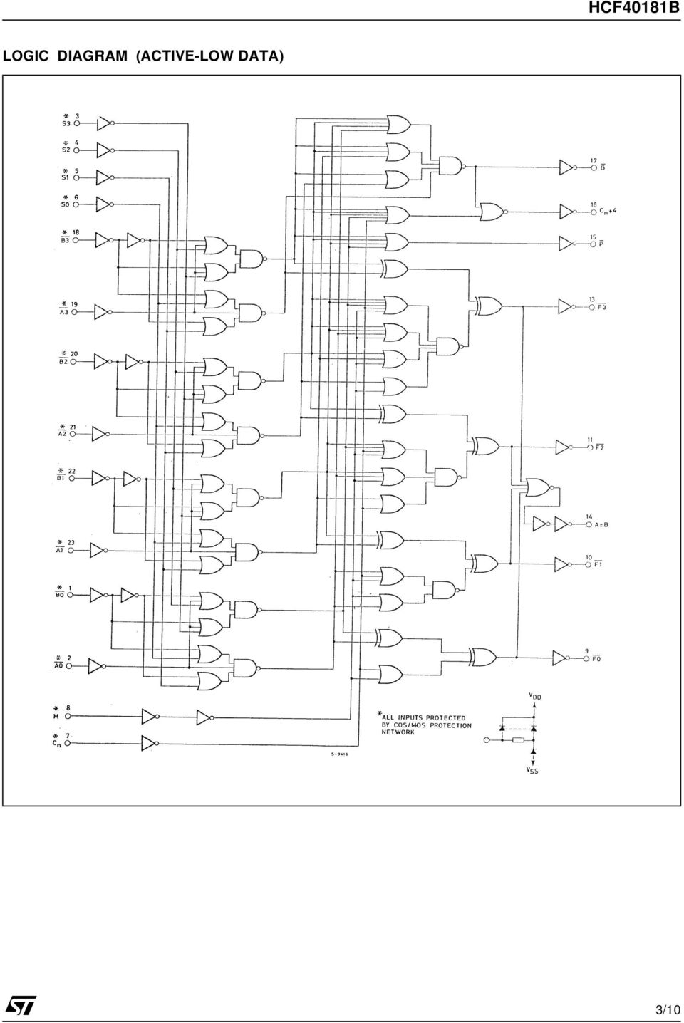
3 LOGIC DIAGRAM (ACTIVE-LOW DATA) 3/10
4 TRUTH TABLE 1 FUNCTION SELECT INPUTS/OUTPUTS ACTIVE LOW INPUTS/OUTPUTS ACTIVE HIGH S3 S1 S2 S0 Logic Function Arithmetic* Function Logic Function Arithmetic* Function (M = H) (M = L, Cn = L) (M = H) (M = L, Cn = H) L L L L A A minus 1 A A L L L H AB AB minus 1 A + B A + B L L H L A + B AB minus 1 AB A + B L L H H Logic 1 minus 1 Logic 0 minus 1 L H L L A + B A plus (A + B) AB A plus AB L H L H B AB plus (A + B) B (A + B) plus AB L H H L A B A minus B minus 1 A B A minus B minus 1 L H H H A + B A + B AB AB minus 1 H L L L AB A plus (A + B) A + B A plus AB H L L H A B A plus B A B A plus B H L H L B AB plus (A + B) B (A + B) plus AB H L H H A + B A + B AB AB minus 1 H H L L Logic 0 A plus A Logic 1 A plus A H H L H AB AB plus A A + B (A + B) plus A H H H L AB AB plus A A + B (A + B) plus A H H H H A A A A minus 1 : Expressed as two s complement. For arithmetic function with Cn in the opposite state, the resulting function is as show plus 1. TRUTH TABLE 2: MAGNITUDE COMPARISON ACTIVE-HIGH DATA ACTIVE-LOW DATA INPUT C n OUTPUT C n + 4 MAGNITUDE INPUT C n OUTPUT C n + 4 MAGNITUDE H H A B L L A B L H A < B H L A < B H L A > B L H A > B L L A B H H A B TRUTH TABLE 3: AC TEST SETUP REFERENCE (ACTIVE-LOW DATA) TEST DELAY TIMES AC PATHS DC DATA INPUTS MODE* INPUTS OUTPUTS TO V SS TO V DD SUM IN to SUM OUT B0 Any F ADD Mode: S0, S3 = V DD ; S1, S2 = V SS. SUBTRACT Mode: S0, S3 = V SS ; S1, S2 = V DD. B1, B2, B3, M, C n All A s ADD SUM IN to P A0 P A1, A2, A3, M, C n All B s ADD SUM IN to G B0 G All A s, M, C n B1, B2, B3 ADD SUM IN to C n + 4 B0 C n + 4 All A s, M, C n B1, B2, B3 ADD C n to SUM OUT C n Any F All A s, M All B s ADD C n to C n +4 C n C n + 4 All A s, M All B s ADD SUM IN to A = B B0 A = B All A s, B1, B2, B3, M C n SUM IN to SUM OUT (logic mode) All B,s Any F All A s, C n M SUBTRACT EXCLUSIVE OR 4/10
 B (A + B) plus AB H L H H A + B A + B AB AB minus 1 H H L L Logic 0 A plus A Logic 1 A plus A H H L H AB AB plus A A + B (A + B) plus A H H H L AB AB plus A A + B (A + B) plus A")
5 ABSOLUTE MAXIMUM RATINGS Symbol Parameter Value Unit V DD Supply Voltage -0.5 to +22 V V I DC Input Voltage -0.5 to V DD V I I DC Input Current ± 10 ma P D Power Dissipation per Package 200 mw Power Dissipation per Output Transistor 100 mw T op Operating Temperature -55 to +125 C T stg Storage Temperature -65 to +150 C Absolute Maximum Ratings are those values beyond which damage to the device may occur. Functional operation under these conditions is not implied. All voltage values are referred to V SS pin voltage. RECOMMENDED OPERATING CONDITIONS Symbol Parameter Value Unit V DD Supply Voltage 3 to 20 V V I Input Voltage 0 to V DD V T op Operating Temperature -55 to 125 C 5/10

6 DC SPECIFICATIONS Test Condition Value Symbol Parameter V I (V) V O (V) I O (µa) V DD (V) T A = 25 C -40 to 85 C -55 to 125 C Min. Typ. Max. Min. Max. Min. Max. Unit I L Quiescent Current 0/ / / / V OH High Level Output 0/5 < Voltage 0/10 < /15 < V OL V IH V IL I OH I OL Low Level Output Voltage High Level Input Voltage Low Level Input Voltage Output Drive Current Output Sink Current 5/0 < /0 < /0 < /4.5 < /9 < /13.5 < /0.5 < /1 < /1.5 < /5 2.5 < /5 4.6 < / < / < /5 0.4 < / < / < I I Input Leakage Current 0/18 Any Input 18 ±10-5 ±0.1 ±1 ±1 µa I OZ 3-State Output Leakage Current 0/18 Any Input 18 ±10-4 ±0.4 ±12 ±12 µa C I Input Capacitance Any Input pf The Noise Margin for both "1" and "0" level is: 1V min. with V DD =5V, 2V min. with V DD =10V, 2.5V min. with V DD =15V µa V V V V ma ma 6/10

7 DYNAMIC ELECTRICAL CHARACTERISTICS (T amb = 25 C, C L = 50pF, R L = 200KΩ, t r = t f = 20 ns) Symbol Parameter Test Condition Value (*) Unit V DD (V) Min. Typ. Max. t PHL t PLH Propagation Delay Time A or B to F (logic mode) A or B to G or P A or B to F, C n+4, or A = B C n to F C n to C n t THL t TLH Transition Time ns ns ns ns ns (*) Typical temperature coefficient for all V DD value is 0.3 %/ C (1) : If more than one unit is cascaded. tr should be made less than or equal to the sum of the transition time and the fixed propagation delay of the output of the driving stage for the estimated capacitive load. TEST CIRCUIT C L = 50pF or equivalent (includes jig and probe capacitance) R L = 200KΩ R T = Z OUT of pulse generator (typically 50Ω) 7/10
 : If more than one unit is cascaded.")
8 WAVEFORM : PROPAGATION DELAY TIMES (f=1mhz; 50% duty cycle) 8/10

9 SO-24 MECHANICAL DATA DIM. mm. inch MIN. TYP MAX. MIN. TYP. MAX. A a a b b C c1 45 (typ.) D E e e F L S 8 (max.) L C c1 a2 A b e3 e s E a1 b1 D F PO13T 9/10
 L C c1 a2 A b e3 e s E a1 b1 D 24 13 F 1 1 2 PO13T 9/10")
10 Information furnished is believed to be accurate and reliable. However, STMicroelectronics assumes no responsibility for the consequences of use of such information nor for any infringement of patents or other rights of third parties which may result from its use. No license is granted by implication or otherwise under any patent or patent rights of STMicroelectronics. Specifications mentioned in this publication are subject to change without notice. This publication supersedes and replaces all information previously supplied. STMicroelectronics products are not authorized for use as critical components in life support devices or systems without express written approval of STMicroelectronics. The ST logo is a registered trademark of STMicroelectronics 2002 STMicroelectronics - Printed in Italy - All Rights Reserved STMicroelectronics GROUP OF COMPANIES Australia - Brazil - Canada - China - Finland - France - Germany - Hong Kong - India - Israel - Italy - Japan - Malaysia - Malta - Morocco Singapore - Spain - Sweden - Switzerland - United Kingdom - United States. 10/10

HCF4001B QUAD 2-INPUT NOR GATE
 QUAD 2-INPUT NOR GATE PROPAGATION DELAY TIME: t PD = 50ns (TYP.) at V DD = 10V C L = 50pF BUFFERED INPUTS AND OUTPUTS STANDARDIZED SYMMETRICAL OUTPUT CHARACTERISTICS QUIESCENT CURRENT SPECIFIED UP TO 20V
HCF4028B BCD TO DECIMAL DECODER
 BCD TO DECIMAL DECODER BCD TO DECIMAL DECODING OR BINARY TO OCTAL DECODING HIGH DECODED OUTPUT DRIVE CAPABILITY "POSITIVE LOGIC" INPUTS AND OUTPUTS: DECODED OUTPUTS GO HIGH ON SELECTION MEDIUM SPEED OPERATION
HCF4010B HEX BUFFER/CONVERTER (NON INVERTING)
") HEX BUFFER/CONVERTER (NON INVERTING) PROPAGATION DELAY TIME: t PD = 50ns (Typ.) at V DD = 10V C L = 50pF HIGH TO LOW LEVEL LOGIC CONVERSION MULTIPLEXER: 1 TO 6 OR 6 TO 1 HIGH "SINK" AND "SOURCE" CURRENT
HEX BUFFER/CONVERTER (NON INVERTING) PROPAGATION DELAY TIME: t PD = 50ns (Typ.) at V DD = 10V C L = 50pF HIGH TO LOW LEVEL LOGIC CONVERSION MULTIPLEXER: 1 TO 6 OR 6 TO 1 HIGH "SINK" AND "SOURCE" CURRENT
Obsolete Product(s) - Obsolete Product(s)
 - Obsolete Product(s)") SYNCHRONOUS PROGRAMMABLE 4-BIT BINARY COUNTER WITH ASYNCHRONOUS CLEAR INTERNAL LOOK-AHEAD FOR FAST COUNTING CARRY OUTPUT FOR CASCADING SYNCHRONOUSLY PROGRAMMABLE LOW-POWER TTL COMPATIBILITY STANDARDIZED
SYNCHRONOUS PROGRAMMABLE 4-BIT BINARY COUNTER WITH ASYNCHRONOUS CLEAR INTERNAL LOOK-AHEAD FOR FAST COUNTING CARRY OUTPUT FOR CASCADING SYNCHRONOUSLY PROGRAMMABLE LOW-POWER TTL COMPATIBILITY STANDARDIZED
HCF4081B QUAD 2 INPUT AND GATE
 QUAD 2 INPUT AND GATE MEDIUM SPEED OPERATION : t PD = 60ns (Typ.) at 10 QUIESCENT CURRENT SPECIFIED UP TO 20 5, 10 AND 15 PARAMETRIC RATINGS INPUT LEAKAGE CURRENT I I = 100nA (MAX) AT DD = 18 T A = 25
HCF4070B QUAD EXCLUSIVE OR GATE
 QUAD EXCLUSIE OR GATE MEDIUM-SPEED OPERATION t PHL = t PLH = 70ns (Typ.) at CL = 50 pf and DD = 10 QUIESCENT CURRENT SPECIFIED UP TO 20 5, 10 AND 15 PARAMETRIC RATINGS INPUT LEAKAGE CURRENT I I = 100nA
HCF4056B BCD TO 7 SEGMENT DECODER /DRIVER WITH STROBED LATCH FUNCTION
 BCD TO 7 SEGMENT DECODER /DRIVER WITH STROBED LATCH FUNCTION QUIESCENT CURRENT SPECIF. UP TO 20V OPERATION OF LIQUID CRYSTALS WITH CMOS CIRCUITS PROVIDES ULTRA LOW POWER DISPLAY. EQUIVALENT AC OUTPUT DRIVE
HCC/HCF4032B HCC/HCF4038B
 HCC/HCF4032B HCC/HCF4038B TRIPLE SERIAL ADDERS INERT INPUTS ON ALL ADDERS FOR SUM COMPLEMENTING APPLICATIONS FULLY STATIC OPERATION...DC TO 10MHz (typ.) @ DD = 10 BUFFERED INPUTS AND OUTPUTS SINGLE-PHASE
Description. Table 1. Device summary. Order code Temperature range Package Packaging Marking
 14-stage ripple carry binary counter/divider and oscillator Applications Automotive Industrial Computer Consumer Description Datasheet - production data Features Medium speed operation Common reset Fully
HCC/HCF4027B DUAL-J-K MASTER-SLAVE FLIP-FLOP
 DUAL-J-K MASTER-SLAVE FLIP-FLOP. SET-RESET CAPABILITY STATIC FLIP-FLOP OPERATION - RETAINS STATE INDEFINITELY WITH CLOCK LEVEL EITHER HIGH OR LOW MEDIUM SPEED OPERATION - 16MHz (typ. clock toggle rate
HCC4541B HCF4541B PROGRAMMABLE TIMER
 HCC4541B HCF4541B PROGRAMMABLE TIMER 16 STAGE BINARI COUNTER LOW SYMMETRICAL OUTPUT RESISTANCE, TYPICALLY 100 OHM AT DD = 15 OSCILLATOR FREQUENCY RANGE : DC TO 100kHz AUTO OR MASTER RESET DISABLES OSCIL-
. MEDIUM SPEED OPERATION - 8MHz (typ.) @ . MULTI-PACKAGE PARALLEL CLOCKING FOR HCC4029B HCF4029B PRESETTABLE UP/DOWN COUNTER BINARY OR BCD DECADE
 @ . MULTI-PACKAGE PARALLEL CLOCKING FOR HCC4029B HCF4029B PRESETTABLE UP/DOWN COUNTER BINARY OR BCD DECADE") HCC4029B HCF4029B PRESETTABLE UP/DOWN COUNTER BINARY OR BCD DECADE. MEDIUM SPEED OPERATION - 8MHz (typ.) @ CL = 50pF AND DD-SS = 10. MULTI-PACKAGE PARALLEL CLOCKING FOR SYNCHRONOUS HIGH SPEED OUTPUT RES-
HCC4029B HCF4029B PRESETTABLE UP/DOWN COUNTER BINARY OR BCD DECADE. MEDIUM SPEED OPERATION - 8MHz (typ.) @ CL = 50pF AND DD-SS = 10. MULTI-PACKAGE PARALLEL CLOCKING FOR SYNCHRONOUS HIGH SPEED OUTPUT RES-
CD4001BC/CD4011BC Quad 2-Input NOR Buffered B Series Gate Quad 2-Input NAND Buffered B Series Gate
 CD4001BC/CD4011BC Quad 2-Input NOR Buffered B Series Gate Quad 2-Input NAND Buffered B Series Gate General Description The CD4001BC and CD4011BC quad gates are monolithic complementary MOS (CMOS) integrated
.LOW POWER DISSIPATION .HIGH NOISE IMMUNITY M74HC154 4 TO 16 LINE DECODER/DEMULTIPLEXER. HIGH SPEED tpd = 15 ns (TYP.) at VCC =5V
 at VCC =5V") . HIGH SPEED tpd = 15 ns (TYP.) at VCC =5V.LOW POWER DISSIPATION I CC =4µA (MAX.) at T A =25 C.HIGH NOISE IMMUNITY VNIH =VNIL =28%VCC (MIN.) OUTPUT DRIVE CAPABILITY 15 LSTTL LOADS SYMMETRICAL OUTPUT IMPEDANCE
. HIGH SPEED tpd = 15 ns (TYP.) at VCC =5V.LOW POWER DISSIPATION I CC =4µA (MAX.) at T A =25 C.HIGH NOISE IMMUNITY VNIH =VNIL =28%VCC (MIN.) OUTPUT DRIVE CAPABILITY 15 LSTTL LOADS SYMMETRICAL OUTPUT IMPEDANCE
Order code Temperature range Package Packaging
 ST485B ST485C Low power RS-485/RS-422 transceiver Features Low quiescent current: 300 µa Designed for RS-485 interface application - 7 V to 12 V common mode input voltage range Driver maintains high impedance
. HIGH SPEED .LOW POWER DISSIPATION .COMPATIBLE WITH TTL OUTPUTS M54HCT27 M74HCT27 TRIPLE 3-INPUT NOR GATE. tpd = 9 ns (TYP.
 M54HCT27 M74HCT27 TRIPLE 3-INPUT NOR GATE. HIGH SPEED tpd = 9 ns (TYP.) AT VCC =5V.LOW POWER DISSIPATION I CC =1µA (MAX.) AT T A =25 C.COMPATIBLE WITH TTL OUTPUTS VIH = 2V (MIN.) VIL = 0.8V (MAX) OUTPUT
CD4013BC Dual D-Type Flip-Flop
 CD4013BC Dual D-Type Flip-Flop General Description The CD4013B dual D-type flip-flop is a monolithic complementary MOS (CMOS) integrated circuit constructed with N- and P-channel enhancement mode transistors.
CD4001BC/CD4011BC Quad 2-Input NOR Buffered B Series Gate Quad 2-Input NAND Buffered B Series Gate
 Quad 2-Input NOR Buffered B Series Gate Quad 2-Input NAND Buffered B Series Gate General Description The CD4001BC and CD4011BC quad gates are monolithic complementary MOS (CMOS) integrated circuits cotructed
Description. Table 1. Device summary. Order code Temperature range Package Packing Marking
 8-bit shift register with output latches (3-state) Applicatio Datasheet - production data SO16 TSSOP16 Automotive Industrial Computer Coumer Features High speed: f MAX = 59 MHz (typ.) at V CC = 6 V Low
CD4008BM CD4008BC 4-Bit Full Adder
 CD4008BM CD4008BC 4-Bit Full Adder General Description The CD4008B types consist of four full-adder stages with fast look-ahead carry provision from stage to stage Circuitry is included to provide a fast
LF00AB/C SERIES VERY LOW DROP VOLTAGE REGULATORS WITH INHIBIT
 LF00AB/C SERIES ERY LOW DROP OLTAGE REGULATORS WITH INHIBIT ERY LOW DROPOUT OLTAGE (5) ERY LOW QUIESCENT CURRENT (TYP. 50 µa IN OFF MODE, 500µA INON MODE) OUTPUT CURRENT UP TO 500 ma LOGIC-CONTROLLED ELECTRONIC
TDA2822 DUAL POWER AMPLIFIER SUPPLY VOLTAGE DOWN TO 3 V LOW CROSSOVER DISTORSION LOW QUIESCENT CURRENT BRIDGE OR STEREO CONFIGURATION
 TDA2822 DUAL POER AMPLIFIER SUPPLY VOLTAGE DON TO 3 V. LO CROSSOVER DISTORSION LO QUIESCENT CURRENT BRIDGE OR STEREO CONFIGURATION DESCRIPTION The TDA2822 is a monolithic integrated circuit in 12+2+2 powerdip,
CD4027BC Dual J-K Master/Slave Flip-Flop with Set and Reset
 October 1987 Revised March 2002 CD4027BC Dual J-K Master/Slave Flip-Flop with Set and Reset General Description The CD4027BC dual J-K flip-flops are monolithic complementary MOS (CMOS) integrated circuits
CD4043BC CD4044BC Quad 3-STATE NOR R/S Latches Quad 3-STATE NAND R/S Latches
 CD4043BC CD4044BC Quad 3-STATE NOR R/S Latches Quad 3-STATE NAND R/S Latches General Description The CD4043BC are quad cross-couple 3-STATE CMOS NOR latches, and the CD4044BC are quad cross-couple 3- STATE
ADJUSTABLE VOLTAGE AND CURRENT REGULATOR
 L200 ADJUSTABLE VOLTAGE AND CURRENT REGULATOR ADJUSTABLE OUTPUT CURRENT UP TO 2 A (GUARANTEED UP TO Tj = 150 C) ADJUSTABLE OUTPUT VOLTAGE DOWN TO 2.85 V INPUT OVERVOLTAGE PROTECTION (UP TO 60 V, 10 ms)
TL084 TL084A - TL084B
 A B GENERAL PURPOSE JFET QUAD OPERATIONAL AMPLIFIERS WIDE COMMONMODE (UP TO V + CC ) AND DIFFERENTIAL VOLTAGE RANGE LOW INPUT BIAS AND OFFSET CURRENT OUTPUT SHORTCIRCUIT PROTECTION HIGH INPUT IMPEDANCE
ST202 5V POWERED MULTI-CHANNEL RS-232 DRIVERS AND RECEIVERS
 5V POWERED MULTI-CHANNEL RS-232 DRIVERS AND RECEIVERS SUPPLY VOLTAGE RANGE: 4.5 TO 5.5V SUPPLY CURRENT NO LOAD (TYP): 1.5mA TRASMITTER OUTPUT VOLTAGE SWING (TYP): ± 9V TRANSITION SLEW RATE (TYP.): 12V/µs
MC14008B. 4-Bit Full Adder
 4-Bit Full Adder The MC4008B 4bit full adder is constructed with MOS PChannel and NChannel enhancement mode devices in a single monolithic structure. This device consists of four full adders with fast
.OPERATING SUPPLY VOLTAGE UP TO 46 V
 L298 DUAL FULL-BRIDGE DRIVER.OPERATING SUPPLY VOLTAGE UP TO 46 V TOTAL DC CURRENT UP TO 4 A. LOW SATURATION VOLTAGE OVERTEMPERATURE PROTECTION LOGICAL "0" INPUT VOLTAGE UP TO 1.5 V (HIGH NOISE IMMUNITY)
MM74HC174 Hex D-Type Flip-Flops with Clear
 Hex D-Type Flip-Flops with Clear General Description The MM74HC174 edge triggered flip-flops utilize advanced silicon-gate CMOS technology to implement D-type flipflops. They possess high noise immunity,
74AC139 74ACT139 Dual 1-of-4 Decoder/Demultiplexer
 Dual 1-of-4 Decoder/Demultiplexer General Description The AC/ACT139 is a high-speed, dual 1-of-4 decoder/ demultiplexer. The device has two independent decoders, each accepting two inputs and providing
STGW40NC60V N-CHANNEL 50A - 600V - TO-247 Very Fast PowerMESH IGBT
 N-CHANNEL 50A - 600V - TO-247 Very Fast PowerMESH IGBT Table 1: General Features STGW40NC60V 600 V < 2.5 V 50 A HIGH CURRENT CAPABILITY HIGH FREQUENCY OPERATION UP TO 50 KHz LOSSES INCLUDE DIODE RECOVERY
LM833 LOW NOISE DUAL OPERATIONAL AMPLIFIER
 LOW NOISE DUAL OPERATIONAL AMPLIFIER LOW VOLTAGE NOISE: 4.5nV/ Hz HIGH GAIN BANDWIDTH PRODUCT: 15MHz HIGH SLEW RATE: 7V/µs LOW DISTORTION:.2% EXCELLENT FREQUENCY STABILITY ESD PROTECTION 2kV DESCRIPTION
IRF740 N-CHANNEL 400V - 0.46Ω - 10A TO-220 PowerMESH II MOSFET
 N-CHANNEL 400V - 0.46Ω - 10A TO-220 PowerMESH II MOSFET TYPE V DSS R DS(on) I D IRF740 400 V < 0.55 Ω 10 A TYPICAL R DS (on) = 0.46Ω EXCEPTIONAL dv/dt CAPABILITY 100% AVALANCHE TESTED LOW GATE CHARGE VERY
CD40174BC CD40175BC Hex D-Type Flip-Flop Quad D-Type Flip-Flop
 Hex D-Type Flip-Flop Quad D-Type Flip-Flop General Description The CD40174BC consists of six positive-edge triggered D- type flip-flops; the true outputs from each flip-flop are externally available. The
4-bit binary full adder with fast carry CIN + (A1 + B1) + 2(A2 + B2) + 4(A3 + B3) + 8(A4 + B4) = = S1 + 2S2 + 4S3 + 8S4 + 16COUT
 + 2(A2 + B2) + 4(A3 + B3) + 8(A4 + B4) = = S1 + 2S2 + 4S3 + 8S4 + 16COUT") Rev. 03 11 November 2004 Product data sheet 1. General description 2. Features The is a high-speed Si-gate CMOS device and is pin compatible with low power Schottky TTL (LSTTL). The is specified in compliance
Rev. 03 11 November 2004 Product data sheet 1. General description 2. Features The is a high-speed Si-gate CMOS device and is pin compatible with low power Schottky TTL (LSTTL). The is specified in compliance
L297 STEPPER MOTOR CONTROLLERS
 L297 STEPPER MOTOR CONTROLLERS NORMAL/WAVE DRIVE HALF/FULL STEP MODES CLOCKWISE/ANTICLOCKWISE DIRECTION SWITCHMODE LOAD CURRENT REGULA- TION PROGRAMMABLE LOAD CURRENT FEW EXTERNAL COMPONENTS RESET INPUT
MM74HC273 Octal D-Type Flip-Flops with Clear
 MM74HC273 Octal D-Type Flip-Flops with Clear General Description The MM74HC273 edge triggered flip-flops utilize advanced silicon-gate CMOS technology to implement D-type flipflops. They possess high noise
ULN2801A, ULN2802A, ULN2803A, ULN2804A
 ULN2801A, ULN2802A, ULN2803A, ULN2804A Eight Darlington array Datasheet production data Features Eight Darlington transistors with common emitters Output current to 500 ma Output voltage to 50 V Integral
. HIGH SPEED .LOW POWER DISSIPATION .HIGH NOISE IMMUNITY M54/M74HC190 M54/M74HC191 4 BIT SYNCHRONOUS UP/DOWN COUNTERS. fmax = 48 MHz (TYP.
 M54/M74HC190 M54/M74HC191 4 BIT SYNCHRONOUS UP/DOWN COUNTERS. HIGH SPEED fmax = 48 MHz (TYP.) AT VCC =5V.LOW POWER DISSIPATION I CC =4µA (MAX.) AT T A =25 C.HIGH NOISE IMMUNITY VNIH =VNIL =28%VCC (MIN.)
74AC138 74ACT138 1-of-8 Decoder/Demultiplexer
 1-of-8 Decoder/Demultiplexer General Description The AC/ACT138 is a high-speed 1-of-8 decoder/demultiplexer. This device is ideally suited for high-speed bipolar memory chip select address decoding. The
STW20NM50 N-CHANNEL 550V @ Tjmax - 0.20Ω - 20ATO-247 MDmesh MOSFET
 N-CHANNEL 550V @ Tjmax - 0.20Ω - 20ATO-247 MDmesh MOSFET TYPE V DSS (@Tjmax) R DS(on) I D STW20NM50 550V < 0.25Ω 20 A TYPICAL R DS (on) = 0.20Ω HIGH dv/dt AND AVALANCHE CAPABILITIES 100% AVALANCHE TESTED
BD241A BD241C. NPN power transistors. Features. Applications. Description. NPN transistors. Audio, general purpose switching and amplifier transistors
 BD241A BD241C NPN power transistors Features. NPN transistors Applications Audio, general purpose switching and amplifier transistors Description The devices are manufactured in Planar technology with
HEF4011B. 1. General description. 2. Features and benefits. 3. Ordering information. 4. Functional diagram. Quad 2-input NAND gate
 Rev. 6 10 December 2015 Product data sheet 1. General description 2. Features and benefits 3. Ordering information The is a quad 2-input NAND gate. The outputs are fully buffered for the highest noise
INTEGRATED CIRCUITS. 74LVC08A Quad 2-input AND gate. Product specification IC24 Data Handbook. 1997 Jun 30
 INTEGRATED CIRCUITS IC24 Data Handbook 1997 Jun 30 FEATURES Wide supply voltage range of 1.2 V to 3.6 V In accordance with JEDEC standard no. 8-1A Inputs accept voltages up to 5.5 V CMOS low power consumption
DM74LS191 Synchronous 4-Bit Up/Down Counter with Mode Control
 August 1986 Revised February 1999 DM74LS191 Synchronous 4-Bit Up/Down Counter with Mode Control General Description The DM74LS191 circuit is a synchronous, reversible, up/ down counter. Synchronous operation
CD4013BC Dual D-Type Flip-Flop
 Dual D-Type Flip-Flop General Description The CD4013B dual D-type flip-flop is a monolithic complementary MOS (CMOS) integrated circuit cotructed with N- and P-channel enhancement mode traistors. Each
TL074 TL074A - TL074B
 A B LOW NOISE JFET QUAD OPERATIONAL AMPLIFIERS WIDE COMMONMODE (UP TO V + CC ) AND DIFFERENTIAL VOLTAGE RANGE LOW INPUT BIAS AND OFFSET CURRENT LOW NOISE e n = 15nV/ Hz (typ) OUTPUT SHORTCIRCUIT PROTECTION
MM74HCT373 MM74HCT374 3-STATE Octal D-Type Latch 3-STATE Octal D-Type Flip-Flop
 3-STATE Octal D-Type Latch 3-STATE Octal D-Type Flip-Flop General Description The MM74HCT373 octal D-type latches and MM74HCT374 Octal D-type flip flops advanced silicongate CMOS technology, which provides
CD4027BM CD4027BC Dual J-K Master Slave Flip-Flop with Set and Reset
 CD4027BM CD4027BC Dual J-K Master Slave Flip-Flop with Set and Reset General Description These dual J-K flip-flops are monolithic complementary MOS (CMOS) integrated circuits constructed with N- and P-
MM74HC4538 Dual Retriggerable Monostable Multivibrator
 MM74HC4538 Dual Retriggerable Monostable Multivibrator General Description The MM74HC4538 high speed monostable multivibrator (one shots) is implemented in advanced silicon-gate CMOS technology. They feature
DDSL01. Secondary protection for DSL lines. Features. Description
 Secondary protection for DSL lines Features Stand off voltage: 30 V Surge capability: I pp = 30 A 8/20 µs Low capacitance device: 4.5 pf at 2 V RoHS package Low leakage current: 0.5 µa at 25 C 3 2 Description
INTEGRATED CIRCUITS. For a complete data sheet, please also download:
 INTEGRATED CIRCUITS DATA SHEET For a complete data sheet, please also download: The IC06 74HC/HCT/HCU/HCMOS Logic Family Specifications The IC06 74HC/HCT/HCU/HCMOS Logic Package Information The IC06 74HC/HCT/HCU/HCMOS
1-of-4 decoder/demultiplexer
 Rev. 6 1 April 2016 Product data sheet 1. General description 2. Features and benefits 3. Applications The contains two 1-of-4 decoders/demultiplexers. Each has two address inputs (na0 and na1, an active
L4940 series VERY LOW DROP 1.5 A REGULATORS
 L4940 series VERY LOW DROP 1.5 A REGULATORS PRECISE 5 V, 8.5 V, 10 V, 12 V OUTPUTS LOW DROPOUT VOLTAGE (500 typ at 1.5A) VERY LOW QUIESCENT CURRENT THERMAL SHUTDOWN SHORT CIRCUIT PROTECTION REVERSE POLARITY
MC33079. Low noise quad operational amplifier. Features. Description
 Low noise quad operational amplifier Datasheet production data Features Low voltage noise: 4.5 nv/ Hz High gain bandwidth product: 15 MHz High slew rate: 7 V/µs Low distortion: 0.002% Large output voltage
MM74HC14 Hex Inverting Schmitt Trigger
 MM74HC14 Hex Inverting Schmitt Trigger General Description The MM74HC14 utilizes advanced silicon-gate CMOS technology to achieve the low power dissipation and high noise immunity of standard CMOS, as
TDA7448 6 CHANNEL VOLUME CONTROLLER 1 FEATURES 2 DESCRIPTION. Figure 1. Package
 6 CHANNEL CONTROLLER FEATURES 6 CHANNEL INPUTS 6 CHANNEL OUTPUTS ATTENUATION RANGE OF 0 TO -79dB CONTROL IN.0dB STEPS 6 CHANNEL INDEPENDENT CONTROL ALL FUNCTION ARE PROGRAMMABLE VIA SERIAL BUS DESCRIPTION
STN3NF06L. N-channel 60 V, 0.07 Ω, 4 A, SOT-223 STripFET II Power MOSFET. Features. Application. Description
 N-channel 60 V, 0.07 Ω, 4 A, SOT-223 STripFET II Power MOSFET Features Type V DSS (@Tjmax) Exceptional dv/dt capability Avalanche rugged technology 100% avalanche tested R DS(on) max STN3NF06L 60 V < 0.1
L78MxxAB L78MxxAC. Precision 500 ma regulators. Features. Description
 L78MxxAB L78MxxAC Precision 500 ma regulators Features Output current to 0.5 A Output voltages of 5; 6; 8; 9; 10; 12; 15; 18; 24 V Thermal overload protection Short circuit protection Output transition
STP80NF55-08 STB80NF55-08 STB80NF55-08-1 N-CHANNEL 55V - 0.0065 Ω - 80A D2PAK/I2PAK/TO-220 STripFET II POWER MOSFET
 STP80NF55-08 STB80NF55-08 STB80NF55-08-1 N-CHANNEL 55V - 0.0065 Ω - 80A D2PAK/I2PAK/TO-220 STripFET II POWER MOSFET TYPE V DSS R DS(on) I D STB80NF55-08/-1 STP80NF55-08 55 V 55 V
VNP5N07 "OMNIFET": FULLY AUTOPROTECTED POWER MOSFET
 "OMNIFET": FULLY AUTOPROTECTED POWER MOSFET TYPE Vclamp RDS(on) Ilim VNP5N07 70 V 0.2 Ω 5 A LINEAR CURRENT LIMITATION THERMAL SHUT DOWN SHORT CIRCUIT PROTECTION INTEGRATED CLAMP LOW CURRENT DRAWN FROM
ULN2001, ULN2002 ULN2003, ULN2004
 ULN2001, ULN2002 ULN2003, ULN2004 Seven Darlington array Datasheet production data Features Seven Darlingtons per package Output current 500 ma per driver (600 ma peak) Output voltage 50 V Integrated suppression
DM74121 One-Shot with Clear and Complementary Outputs
 June 1989 Revised July 2001 DM74121 One-Shot with Clear and Complementary Outputs General Description The DM74121 is a monostable multivibrator featuring both positive and negative edge triggering with
LM134-LM234-LM334. Three terminal adjustable current sources. Features. Description
 Three terminal adjustable current sources Features Operates from 1V to 40V 0.02%/V current regulation Programmable from 1µA to 10mA ±3% initial accuracy Description The LM134/LM234/LM334 are 3-terminal
Description SO-8. series. Furthermore, in the 8-pin configuration Very low-dropout voltage (0.2 V typ.)
") ery low-dropout voltage regulator with inhibit function TO-92 Bag TO-92 Tape and reel Ammopack 1 2 3 SO-8 Description Datasheet - production data The is a very low-dropout voltage regulator available in
ery low-dropout voltage regulator with inhibit function TO-92 Bag TO-92 Tape and reel Ammopack 1 2 3 SO-8 Description Datasheet - production data The is a very low-dropout voltage regulator available in
L293B L293E PUSH-PULL FOUR CHANNEL DRIVERS. OUTPUT CURRENT 1A PER CHANNEL PEAK OUTPUT CURRENT 2A PER CHANNEL (non repetitive) INHIBIT FACILITY
 INHIBIT FACILITY") L293B L293E PUSH-PULL FOUR CHANNEL DRIVERS OUTPUT CURRENT 1A PER CHANNEL PEAK OUTPUT CURRENT 2A PER CHANNEL (non repetitive) INHIBIT FACILITY. HIGH NOISE IMMUNITY SEPARATE LOGIC SUPPLY OVERTEMPERATURE
L293B L293E PUSH-PULL FOUR CHANNEL DRIVERS OUTPUT CURRENT 1A PER CHANNEL PEAK OUTPUT CURRENT 2A PER CHANNEL (non repetitive) INHIBIT FACILITY. HIGH NOISE IMMUNITY SEPARATE LOGIC SUPPLY OVERTEMPERATURE
2STBN15D100. Low voltage NPN power Darlington transistor. Features. Application. Description
 Low voltage NPN power Darlington transistor Features Good h FE linearity High f T frequency Monolithic Darlington configuration with integrated antiparallel collector-emitter diode TAB Application Linear
Symbol Parameter Value Unit V DS Drain-source Voltage (V GS =0) 50 V V DGR Drain- gate Voltage (R GS =20kΩ) 50 V
 50 V V DGR Drain- gate Voltage (R GS =20kΩ) 50 V") BUZ71A N - CHANNEL 50V - 0.1Ω - 13A TO-220 STripFET POWER MOSFET TYPE V DSS R DS(on) I D BUZ71A 50 V < 0.12 Ω 13 A TYPICAL RDS(on) = 0.1 Ω AVALANCHE RUGGED TECHNOLOGY 100% AVALANCHE TESTED HIGH CURRENT
BUZ71A N - CHANNEL 50V - 0.1Ω - 13A TO-220 STripFET POWER MOSFET TYPE V DSS R DS(on) I D BUZ71A 50 V < 0.12 Ω 13 A TYPICAL RDS(on) = 0.1 Ω AVALANCHE RUGGED TECHNOLOGY 100% AVALANCHE TESTED HIGH CURRENT
STP60NF06FP. N-channel 60V - 0.014Ω - 30A TO-220FP STripFET II Power MOSFET. General features. Description. Internal schematic diagram.
 N-channel 60V - 0.014Ω - 30A TO-220FP STripFET II Power MOSFET General features Type V DSS R DS(on) I D STP60NF06FP 60V
1-800-831-4242
 Distributed by: www.jameco.com 1-800-831-4242 The content and copyrights of the attached material are the property of its owner. DM74LS161A DM74LS163A Synchronous 4-Bit Binary Counters General Description
DM74LS00 Quad 2-Input NAND Gate
 DM74LS00 Quad 2-Input NAND Gate General Description This device contains four independent gates each of which performs the logic NAND function. Ordering Code: August 1986 Revised March 2000 Order Number
BD238. Low voltage PNP power transistor. Features. Applications. Description. Low saturation voltage PNP transistor
 Low voltage PNP power transistor Features Low saturation voltage PNP transistor Applications Audio, power linear and switching applications Description The device is manufactured in planar technology with
LM337. Three-terminal adjustable negative voltage regulators. Features. Description
 Three-terminal adjustable negative voltage regulators Datasheet - production data current limit, thermal overload protection and safe area protection. All overload protection circuitry remains fully functional
Symbol Parameter Value Unit V i-o Input-output Differential Voltage 40 V I O Output Current Intenrally Limited Top
 LM117/217 LM317 1.2V TO 37V VOLTAGE REGULATOR OUTPUT VOLTAGE RANGE : 1.2 TO 37V OUTPUT CURRENT IN EXCESS OF 1.5A 0.1% LINE AND LOAD REGULATION FLOATING OPERATION FOR HIGH VOLTAGES COMPLETE SERIES OF PROTECTIONS
STM6315. Open drain microprocessor reset. Features
 Open drain microprocessor reset Features Low supply current of 1.5µA (typ) ±1.8% reset threshold accuracy (25 C) Guaranteed RST assertion down to V CC = 1.0V Open drain RST output can exceed V CC Power
STP60NF06. N-channel 60V - 0.014Ω - 60A TO-220 STripFET II Power MOSFET. General features. Description. Internal schematic diagram.
 N-channel 60V - 0.014Ω - 60A TO-220 STripFET II Power MOSFET General features Type V DSS R DS(on) I D STP60NF06 60V
BUX48/48A BUV48A/V48AFI
 BUX48/48A BU48A/48AFI HIGH POWER NPN SILICON TRANSISTORS STMicroelectronics PREFERRED SALESTYPES NPN TRANSISTOR HIGH OLTAGE CAPABILITY HIGH CURRENT CAPABILITY FAST SWITCHING SPEED APPLICATIONS SWITCH MODE
Description. Table 1. Device summary
 2 A positive voltage regulator IC Description Datasheet - production data Features TO-220 Output current up to 2 A Output voltages of 5; 7.5; 9; 10; 12; 15; 18; 24 V Thermal protection Short circuit protection
DM74LS169A Synchronous 4-Bit Up/Down Binary Counter
 Synchronous 4-Bit Up/Down Binary Counter General Description This synchronous presettable counter features an internal carry look-ahead for cascading in high-speed counting applications. Synchronous operation
Table 1. Absolute maximum ratings (T amb = 25 C) Symbol Parameter Value Unit. ISO 10605 - C = 330 pf, R = 330 Ω : Contact discharge Air discharge
 Symbol Parameter Value Unit. ISO 10605 - C = 330 pf, R = 330 Ω : Contact discharge Air discharge") Automotive dual-line Transil, transient voltage suppressor (TVS) for CAN bus Datasheet - production data Complies with the following standards ISO 10605 - C = 150 pf, R = 330 Ω : 30 kv (air discharge)
Automotive dual-line Transil, transient voltage suppressor (TVS) for CAN bus Datasheet - production data Complies with the following standards ISO 10605 - C = 150 pf, R = 330 Ω : 30 kv (air discharge)
DM74184 DM74185A BCD-to-Binary and Binary-to-BCD Converters
 DM74184 DM74185A BCD-to-Binary and Binary-to-BCD Converters General Description These monolithic converters are derived from the 256-bit read only memories DM5488 and DM7488 Emitter connections are made
74AC191 Up/Down Counter with Preset and Ripple Clock
 74AC191 Up/Down Counter with Preset and Ripple Clock General Description The AC191 is a reversible modulo 16 binary counter. It features synchronous counting and asynchronous presetting. The preset feature
DM74LS151 1-of-8 Line Data Selector/Multiplexer
 1-of-8 Line Data Selector/Multiplexer General Description This data selector/multiplexer contains full on-chip decoding to select the desired data source. The DM74LS151 selects one-of-eight data sources.
Quad 2-input NAND Schmitt trigger
 Rev. 9 15 December 2015 Product data sheet 1. General description 2. Features and benefits 3. Applications The is a quad two-input NAND gate. Each input has a Schmitt trigger circuit. The gate switches
STW34NB20 N-CHANNEL 200V - 0.062 Ω - 34A TO-247 PowerMESH MOSFET
 N-CHANNEL 200V - 0.062 Ω - 34A TO-247 PowerMESH MOSFET Table 1. General Features Figure 1. Package Type V DSS R DS(on) I D STW34NB20 200 V < 0.075 Ω 34 A FEATURES SUMMARY TYPICAL R DS(on) = 0.062 Ω EXTREMELY
5495A DM7495 4-Bit Parallel Access Shift Registers
 5495A DM7495 4-Bit Parallel Access Shift Registers General Description These 4-bit registers feature parallel and serial inputs parallel outputs mode control and two clock inputs The registers have three
CD4511BM CD4511BC BCD-to-7 Segment Latch Decoder Driver
 CD4511BM CD4511BC BCD-to-7 Segment Latch Decoder Driver General Description The CD4511BM CD4511BC BCD-to-seven segment latch decoder driver is constructed with complementary MOS (CMOS) enhancement mode
STP62NS04Z N-CHANNEL CLAMPED 12.5mΩ - 62A TO-220 FULLY PROTECTED MESH OVERLAY MOSFET
 N-CHANNEL CLAMPED 12.5mΩ - 62A TO-220 FULLY PROTECTED MESH OVERLAY MOSFET TYPE V DSS R DS(on) I D STP62NS04Z CLAMPED
SG2525A SG3525A REGULATING PULSE WIDTH MODULATORS
 SG2525A SG3525A REGULATING PULSE WIDTH MODULATORS 8 TO 35 V OPERATION 5.1 V REFERENCE TRIMMED TO ± 1 % 100 Hz TO 500 KHz OSCILLATOR RANGE SEPARATE OSCILLATOR SYNC TERMINAL ADJUSTABLE DEADTIME CONTROL INTERNAL
ESDLIN1524BJ. Transil, transient voltage surge suppressor diode for ESD protection. Features. Description SOD323
 Transil, transient voltage surge suppressor diode for ESD protection Datasheet production data Features Max peak pulse power 160 W (8/0 µs) Asymmetrical bidirectional device Stand-off voltage: 15 and 4
3-to-8 line decoder, demultiplexer with address latches
 Rev. 7 29 January 2016 Product data sheet 1. General description The is a high-speed Si-gate CMOS device and is pin compatible with low-power Schottky TTL (LSTTL). The is specified in compliance with JEDEC
L78M00 SERIES POSITIVE VOLTAGE REGULATORS. www.tvsat.com.pl
 SERIES POSITIVE VOLTAGE REGULATORS OUTPUT CURRENT TO 0.5A OUTPUT VOLTAGES OF 5; 6; 8; 9; 10; 12; 15; 18; 20; 24V THERMAL OVERLOAD PROTECTION SHORT CIRCUIT PROTECTION OUTPUT TRANSISTOR SOA PROTECTION DESCRIPTION
DM74LS193 Synchronous 4-Bit Binary Counter with Dual Clock
 September 1986 Revised March 2000 DM74LS193 Synchronous 4-Bit Binary Counter with Dual Clock General Description The DM74LS193 circuit is a synchronous up/down 4-bit binary counter. Synchronous operation
CD4093BM CD4093BC Quad 2-Input NAND Schmitt Trigger
 CD4093BM CD4093BC Quad 2-Input NAND Schmitt Trigger General Description The CD4093B consists of four Schmitt-trigger circuits Each circuit functions as a 2-input NAND gate with Schmitt-trigger action on
BD135 - BD136 BD139 - BD140
 BD135 - BD136 BD139 - BD140 Complementary low voltage transistor Features Products are pre-selected in DC current gain Application General purpose Description These epitaxial planar transistors are mounted
STP55NF06L STB55NF06L - STB55NF06L-1
 General features STP55NF06L STB55NF06L - STB55NF06L-1 N-channel 60V - 0.014Ω - 55A TO-220/D 2 PAK/I 2 PAK STripFET II Power MOSFET Type V DSS R DS(on) I D STP55NF06L 60V
UA741. General-purpose single operational amplifier. Features. Applications. Description. N DIP8 (plastic package)
") General-purpose single operational amplifier Datasheet - production data N DIP8 (plastic package) D SO8 (plastic micropackage) Pin connections (top view) 1 - Offset null 1 2 - Inverting input 3 - Non-inverting
General-purpose single operational amplifier Datasheet - production data N DIP8 (plastic package) D SO8 (plastic micropackage) Pin connections (top view) 1 - Offset null 1 2 - Inverting input 3 - Non-inverting
5485 DM5485 DM7485 4-Bit Magnitude Comparators
 5485 DM5485 DM7485 4-Bit Magnitude Comparators General Description These 4-bit magnitude comparators perform comparison of straight binary or BCD codes Three fully-decoded decisions about two 4-bit words
MC34063A MC34063E DC-DC CONVERTER CONTROL CIRCUITS
 MC34063A MC34063E DC-DC CONVERTER CONTROL CIRCUITS OUTPUT SWITCH CURRENT IN EXCESS OF 1.5A 2% REFERENCE ACCURACY LOW QUIESCENT CURRENT: 2.5mA (TYP.) OPERATING FROM 3V TO 40V FREQUENCY OPERATION TO 100KHz