ENEE 307 Electronic Circuit Design Laboratory Spring A. Iliadis Electrical Engineering Department University of Maryland College Park MD 20742
|
|
|
- Anastasia Lynch
- 7 years ago
- Views:
Transcription
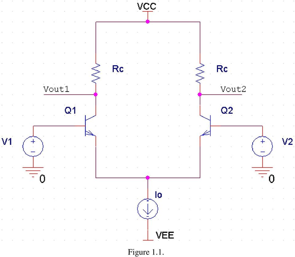
1 1.1. Differential Amplifiers ENEE 307 Electronic Circuit Design Laboratory Spring 2012 A. Iliadis Electrical Engineering Department University of Maryland College Park MD Differential Amplifiers Differential amplifiers are the heart of most circuits today and can be used as pre-amplification stages, Op-Amps, modulators-demodulators, sensor elements etc. Before coming to this lab you should have your PSPICE design ready to show to your TA And have studied Differential Amps in Chapter 8 (pp , ) of Sedra and Smith 6 th Edition. Include your PSPICE design results in your report. In this Lab you are required to design using SPICE a single stage and a double stage differential amp, build the circuit, and measure the characteristics of the final version of the circuit. The 3904 npn BJT will be your active transistor element and you may choose any passive component values given by PSPICE (resistor, capacitors etc) and that you deem appropriate to make your circuit work under the given specifications. The diff amp generates an output signal proportional to the difference between the two independent input signals. It consists basically of two MATCHED transistors biased by a current source which is another transistor usually part of a current mirror, as shown in Fig It is important therefore, when you build your circuit to make sure that you use two transistors with closely matched betas. This you will accomplish by measuring the transistors characteristics in the curve tracer or by simply using a multimeter to measure beta. Before coming to the lab, study the diff amps and current mirrors in the reference books of your course outline. Then use SPICE at the lab to design your circuit. Produce theoretical (PSPICE) inputoutput signal characteristics using sinusoidal signals, single ended output differential and common mode gains, differential output differential and common mode gains, and the common mode rejection ratio CMRR. Realize your circuit and measure same quantities as above. Compare your theoretical and experimental results. Explain discrepancies. Reviewing the definitions of the diff-amp parameters, v 1 and v 2 input voltages can be expressed in differential and common mode as: v id = v 1 - v 2 and v ic = [v 1 + v 2 ]/2 [1.1.1]
 of Sedra and Smith 6 th Edition.")
2 And it follows that for pure differential input (i.e. v ic = 0 ) v 1 = - v 2, and for pure common mode input (i.e. v id = 0) v 1 = v 2. The gain expressions are derived the usual small signal linear analysis, and once the gains are known then the output voltages can be found for any combination of v 1 and v 2. Two different types of gain can be extracted: 1. The single-ended differential mode output gain A d1 and A d2, measured at each output terminal and the ground is given as: A d1 = - g m R C /2 and A d2 = + g m R C /2 [1.1.2] The single-ended common mode output gain A c1 and A c2, measured at each output terminal and the ground is given as: A c1 = - [g m R C ]/[1+2 g m r oc ] and A c2 = - [g m R C ]/[1+2 g m r oc ] [1.1.3] where r oc is the resistance of your current bias i.e. the resistance of transistor Q 3 of the current mirror. 2. The differential (measured between the two output terminals) differential mode output given as: A dd = A d1 - A d2 = g m R C and [1.1.4] the differential (measured between the two output terminals) common mode output given as: A cd = A c1 - A c2 = 0 [1.1.5] [1.1.4],[1.1.5] are valid only if the two collector resistances are exactly equal. The primary function of the diff-amp is to enhance the difference between the two inputs and supress the common mode component. Hence a figure of merit for the diff-amp is the common-mode rejection ratio which must be as large as possible and it is defined as follows: CMRR = 20log A d / A c [1.1.6] 1.2. Single stage diff-amp Design and build a single stage diff-amp (Fig. 1.1) with a linear output response in the frequency range of 20Hz to 20KHz. Use V CC = 10V and V EE = -10V Measure voltages and currents, diff and common mode gains, open and closed circuit gains, CMRR, and frequency response What can you change in the simple circuit to significantly improve its gain? (Current mirror

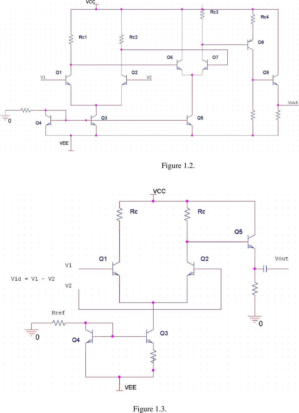
3 active load) Multistage diff-amp Design and build a two stage diff-amp (Fig. 1.2) with a linear output response in the frequency range of 20Hz to 20KHz. Target a minimum open circuit voltage gain of 1000 V/V, and a closedcircuit gain of 100 V/V. Design for low power consumption Measure the parameters of your circuit as above What approach would you take to increase the frequency range of your diff-amp? 1.4. Design a simple op-amp Design and build a simple op-amp circuit (Fig. 1.3) with the same specs as your single stage diff-amp Measure the parameters and characteristics of the op-amp Extra credit: Design and build a non-inverting Miller integrator: v o (t) = 2/RC_v i (t) dt Design and build a full-wave rectifier.
 with the same specs as your single stage diff-amp. 1.4.2. Measure the parameters and characteristics of the op-amp. 1.5. Extra credit: 1.5.1. Design and build a non-inverting Miller integrator: v o (t) = 2/RC_v i (t) dt.")
4 Figure 1.1.
5 Figure

6 Figure 1.3. Figure 1.2.
LABORATORY 2 THE DIFFERENTIAL AMPLIFIER
 LABORATORY 2 THE DIFFERENTIAL AMPLIFIER OBJECTIVES 1. To understand how to amplify weak (small) signals in the presence of noise. 1. To understand how a differential amplifier rejects noise and common
Objectives The purpose of this lab is build and analyze Differential amplifiers based on NPN transistors (or NMOS transistors).
.") 1 Lab 03: Differential Amplifiers (BJT) (20 points) NOTE: 1) Please use the basic current mirror from Lab01 for the second part of the lab (Fig. 3). 2) You can use the same chip as the basic current mirror;
1 Lab 03: Differential Amplifiers (BJT) (20 points) NOTE: 1) Please use the basic current mirror from Lab01 for the second part of the lab (Fig. 3). 2) You can use the same chip as the basic current mirror;
Chapter 8 Differential and Multistage Amplifiers. EE 3120 Microelectronics II
 1 Chapter 8 Differential and Multistage Amplifiers Operational Amplifier Circuit Components 2 1. Ch 7: Current Mirrors and Biasing 2. Ch 9: Frequency Response 3. Ch 8: Active-Loaded Differential Pair 4.
CHAPTER 10 OPERATIONAL-AMPLIFIER CIRCUITS
 CHAPTER 10 OPERATIONAL-AMPLIFIER CIRCUITS Chapter Outline 10.1 The Two-Stage CMOS Op Amp 10.2 The Folded-Cascode CMOS Op Amp 10.3 The 741 Op-Amp Circuit 10.4 DC Analysis of the 741 10.5 Small-Signal Analysis
Transistor Characteristics and Single Transistor Amplifier Sept. 8, 1997
 Physics 623 Transistor Characteristics and Single Transistor Amplifier Sept. 8, 1997 1 Purpose To measure and understand the common emitter transistor characteristic curves. To use the base current gain
3.4 - BJT DIFFERENTIAL AMPLIFIERS
 BJT Differential Amplifiers (6/4/00) Page 1 3.4 BJT DIFFERENTIAL AMPLIFIERS INTRODUCTION Objective The objective of this presentation is: 1.) Define and characterize the differential amplifier.) Show the
Physics 623 Transistor Characteristics and Single Transistor Amplifier Sept. 13, 2006
 Physics 623 Transistor Characteristics and Single Transistor Amplifier Sept. 13, 2006 1 Purpose To measure and understand the common emitter transistor characteristic curves. To use the base current gain
Lecture 18: Common Emitter Amplifier. Maximum Efficiency of Class A Amplifiers. Transformer Coupled Loads.
 Whites, EE 3 Lecture 18 Page 1 of 10 Lecture 18: Common Emitter Amplifier. Maximum Efficiency of Class A Amplifiers. Transformer Coupled Loads. We discussed using transistors as switches in the last lecture.
MAS.836 HOW TO BIAS AN OP-AMP
 MAS.836 HOW TO BIAS AN OP-AMP Op-Amp Circuits: Bias, in an electronic circuit, describes the steady state operating characteristics with no signal being applied. In an op-amp circuit, the operating characteristic
The BJT Differential Amplifier. Basic Circuit. DC Solution
 c Copyright 010. W. Marshall Leach, Jr., Professor, Georgia Institute of Technology, School of Electrical and Computer Engineering. The BJT Differential Amplifier Basic Circuit Figure 1 shows the circuit
Chapter 12: The Operational Amplifier
 Chapter 12: The Operational Amplifier 12.1: Introduction to Operational Amplifier (Op-Amp) Operational amplifiers (op-amps) are very high gain dc coupled amplifiers with differential inputs; they are used
Frequency Response of Filters
 School of Engineering Department of Electrical and Computer Engineering 332:224 Principles of Electrical Engineering II Laboratory Experiment 2 Frequency Response of Filters 1 Introduction Objectives To
Laboratory 4: Feedback and Compensation
 Laboratory 4: Feedback and Compensation To be performed during Week 9 (Oct. 20-24) and Week 10 (Oct. 27-31) Due Week 11 (Nov. 3-7) 1 Pre-Lab This Pre-Lab should be completed before attending your regular
OPERATIONAL AMPLIFIERS. o/p
 OPERATIONAL AMPLIFIERS 1. If the input to the circuit of figure is a sine wave the output will be i/p o/p a. A half wave rectified sine wave b. A fullwave rectified sine wave c. A triangular wave d. A
OBJECTIVE QUESTIONS IN ANALOG ELECTRONICS
 1. The early effect in a bipolar junction transistor is caused by (a) fast turn-on (c) large collector-base reverse bias (b)fast turn-off (d) large emitter-base forward bias 2. MOSFET can be used as a
Common Base BJT Amplifier Common Collector BJT Amplifier
 Common Base BJT Amplifier Common Collector BJT Amplifier Common Collector (Emitter Follower) Configuration Common Base Configuration Small Signal Analysis Design Example Amplifier Input and Output Impedances
Operational Amplifier - IC 741
 Operational Amplifier - IC 741 Tabish December 2005 Aim: To study the working of an 741 operational amplifier by conducting the following experiments: (a) Input bias current measurement (b) Input offset
Unit/Standard Number. High School Graduation Years 2010, 2011 and 2012
 1 Secondary Task List 100 SAFETY 101 Demonstrate an understanding of State and School safety regulations. 102 Practice safety techniques for electronics work. 103 Demonstrate an understanding of proper
Op amp DC error characteristics and the effect on high-precision applications
 Op amp DC error characteristics and the effect on high-precision applications Srudeep Patil, Member of Technical Staff, Maxim Integrated - January 01, 2014 This article discusses the DC limitations of
Electronics. Discrete assembly of an operational amplifier as a transistor circuit. LD Physics Leaflets P4.2.1.1
 Electronics Operational Amplifier Internal design of an operational amplifier LD Physics Leaflets Discrete assembly of an operational amplifier as a transistor circuit P4.2.1.1 Objects of the experiment
Content Map For Career & Technology
 Content Strand: Applied Academics CT-ET1-1 analysis of electronic A. Fractions and decimals B. Powers of 10 and engineering notation C. Formula based problem solutions D. Powers and roots E. Linear equations
Analog Signal Conditioning
 Analog Signal Conditioning Analog and Digital Electronics Electronics Digital Electronics Analog Electronics 2 Analog Electronics Analog Electronics Operational Amplifiers Transistors TRIAC 741 LF351 TL084
School of Engineering Department of Electrical and Computer Engineering
 1 School of Engineering Department of Electrical and Computer Engineering 332:223 Principles of Electrical Engineering I Laboratory Experiment #4 Title: Operational Amplifiers 1 Introduction Objectives
Current vs. Voltage Feedback Amplifiers
 Current vs. ltage Feedback Amplifiers One question continuously troubles the analog design engineer: Which amplifier topology is better for my application, current feedback or voltage feedback? In most
LAB VII. BIPOLAR JUNCTION TRANSISTOR CHARACTERISTICS
 LAB VII. BIPOLAR JUNCTION TRANSISTOR CHARACTERISTICS 1. OBJECTIVE In this lab, you will study the DC characteristics of a Bipolar Junction Transistor (BJT). 2. OVERVIEW You need to first identify the physical
LAB VIII. BIPOLAR JUNCTION TRANSISTOR CHARACTERISTICS
 LAB VIII. BIPOLAR JUNCTION TRANSISTOR CHARACTERISTICS 1. OBJECTIVE In this lab, you will study the DC characteristics of a Bipolar Junction Transistor (BJT). 2. OVERVIEW In this lab, you will inspect the
6.101 Final Project Report Class G Audio Amplifier
 6.101 Final Project Report Class G Audio Amplifier Mark Spatz 4/3/2014 1 1 Introduction For my final project, I designed and built a 150 Watt audio amplifier to replace the underpowered and unreliable
Lab #9: AC Steady State Analysis
 Theory & Introduction Lab #9: AC Steady State Analysis Goals for Lab #9 The main goal for lab 9 is to make the students familar with AC steady state analysis, db scale and the NI ELVIS frequency analyzer.
Common Emitter BJT Amplifier Design Current Mirror Design
 Common Emitter BJT Amplifier Design Current Mirror Design 1 Some Random Observations Conditions for stabilized voltage source biasing Emitter resistance, R E, is needed. Base voltage source will have finite
Differential Amplifier Offset. Causes of dc voltage and current offset Modeling dc offset R C
 ESE39 ntroduction to Microelectronics Differential Amplifier Offset Causes of dc voltage and current offset Modeling dc offset mismatch S mismatch β mismatch transistor mismatch dc offsets in differential
Lab 7: Operational Amplifiers Part I
 Lab 7: Operational Amplifiers Part I Objectives The objective of this lab is to study operational amplifier (op amp) and its applications. We will be simulating and building some basic op amp circuits,
Fig. 1 :Block diagram symbol of the operational amplifier. Characteristics ideal op-amp real op-amp
 Experiment: General Description An operational amplifier (op-amp) is defined to be a high gain differential amplifier. When using the op-amp with other mainly passive elements, op-amp circuits with various
BJT Characteristics and Amplifiers
 BJT Characteristics and Amplifiers Matthew Beckler beck0778@umn.edu EE2002 Lab Section 003 April 2, 2006 Abstract As a basic component in amplifier design, the properties of the Bipolar Junction Transistor
Transistor Amplifiers
 Physics 3330 Experiment #7 Fall 1999 Transistor Amplifiers Purpose The aim of this experiment is to develop a bipolar transistor amplifier with a voltage gain of minus 25. The amplifier must accept input
Bipolar Transistor Amplifiers
 Physics 3330 Experiment #7 Fall 2005 Bipolar Transistor Amplifiers Purpose The aim of this experiment is to construct a bipolar transistor amplifier with a voltage gain of minus 25. The amplifier must
ANADOLU UNIVERSITY DEPARTMENT OF ELECTRICAL AND ELECTRONICS ENGINEERING
 ANADOLU UNIVERSITY DEPARTMENT OF ELECTRICAL AND ELECTRONICS ENGINEERING EEM 102 INTRODUCTION TO ELECTRICAL ENGINEERING EXPERIMENT 9: DIODES AND DC POWER SUPPLY OBJECTIVE: To observe how a diode functions
LM 358 Op Amp. If you have small signals and need a more useful reading we could amplify it using the op amp, this is commonly used in sensors.
 LM 358 Op Amp S k i l l L e v e l : I n t e r m e d i a t e OVERVIEW The LM 358 is a duel single supply operational amplifier. As it is a single supply it eliminates the need for a duel power supply, thus
Lab 5 Operational Amplifiers
 Lab 5 Operational Amplifiers By: Gary A. Ybarra Christopher E. Cramer Duke University Department of Electrical and Computer Engineering Durham, NC. Purpose The purpose of this lab is to examine the properties
Common-Emitter Amplifier
 Common-Emitter Amplifier A. Before We Start As the title of this lab says, this lab is about designing a Common-Emitter Amplifier, and this in this stage of the lab course is premature, in my opinion,
TS321 Low Power Single Operational Amplifier
 SOT-25 Pin Definition: 1. Input + 2. Ground 3. Input - 4. Output 5. Vcc General Description The TS321 brings performance and economy to low power systems. With high unity gain frequency and a guaranteed
Fully Differential CMOS Amplifier
 ECE 511 Analog Electronics Term Project Fully Differential CMOS Amplifier Saket Vora 6 December 2006 Dr. Kevin Gard NC State University 1 Introduction In this project, a fully differential CMOS operational
LAB 12: ACTIVE FILTERS
 A. INTRODUCTION LAB 12: ACTIVE FILTERS After last week s encounter with op- amps we will use them to build active filters. B. ABOUT FILTERS An electric filter is a frequency-selecting circuit designed
Lecture 30: Biasing MOSFET Amplifiers. MOSFET Current Mirrors.
 Whites, EE 320 Lecture 30 Page 1 of 8 Lecture 30: Biasing MOSFET Amplifiers. MOSFET Current Mirrors. There are two different environments in which MOSFET amplifiers are found, (1) discrete circuits and
Rectifier circuits & DC power supplies
 Rectifier circuits & DC power supplies Goal: Generate the DC voltages needed for most electronics starting with the AC power that comes through the power line? 120 V RMS f = 60 Hz T = 1667 ms) = )sin How
Pulse Width Modulation (PWM) LED Dimmer Circuit. Using a 555 Timer Chip
 LED Dimmer Circuit. Using a 555 Timer Chip") Pulse Width Modulation (PWM) LED Dimmer Circuit Using a 555 Timer Chip Goals of Experiment Demonstrate the operation of a simple PWM circuit that can be used to adjust the intensity of a green LED by varying
Pulse Width Modulation (PWM) LED Dimmer Circuit Using a 555 Timer Chip Goals of Experiment Demonstrate the operation of a simple PWM circuit that can be used to adjust the intensity of a green LED by varying
Lecture 060 Push-Pull Output Stages (1/11/04) Page 060-1. ECE 6412 - Analog Integrated Circuits and Systems II P.E. Allen - 2002
 Page 060-1. ECE 6412 - Analog Integrated Circuits and Systems II P.E. Allen - 2002") Lecture 060 PushPull Output Stages (1/11/04) Page 0601 LECTURE 060 PUSHPULL OUTPUT STAGES (READING: GHLM 362384, AH 226229) Objective The objective of this presentation is: Show how to design stages that
Lecture 060 PushPull Output Stages (1/11/04) Page 0601 LECTURE 060 PUSHPULL OUTPUT STAGES (READING: GHLM 362384, AH 226229) Objective The objective of this presentation is: Show how to design stages that
Bipolar Junction Transistors
 Bipolar Junction Transistors Physical Structure & Symbols NPN Emitter (E) n-type Emitter region p-type Base region n-type Collector region Collector (C) B C Emitter-base junction (EBJ) Base (B) (a) Collector-base
LABORATORY MANUAL DEPARTMENT OF ELECTRICAL & COMPUTER ENGINEERING
 LABORATORY MANUAL DEPARTMENT OF ELECTRICAL & COMPUTER ENGINEERING UNIVERSITY OF CENTRAL FLORIDA EEL 4309 Electronics II Revised January 2012 Table of Contents Safety: Introduction: Experiment #1: Experiment
Bipolar Junction Transistor Basics
 by Kenneth A. Kuhn Sept. 29, 2001, rev 1 Introduction A bipolar junction transistor (BJT) is a three layer semiconductor device with either NPN or PNP construction. Both constructions have the identical
AC 2009-2024: STUDENT OUTLOOK TOWARD MEDIA-BASED MODULES IN ELECTRONICS AND NETWORK ANALYSIS
 AC 2009-2024: STUDENT OUTLOOK TOWARD MEDIA-BASED MODULES IN ELECTRONICS AND NETWORK ANALYSIS Jean-Claude Thomassian, State University of New York, Maritime College Dr. Jean-Claude Thomassian received his
Diode Circuits. Operating in the Reverse Breakdown region. (Zener Diode)
") Diode Circuits Operating in the Reverse Breakdown region. (Zener Diode) In may applications, operation in the reverse breakdown region is highly desirable. The reverse breakdown voltage is relatively insensitive
Diode Circuits Operating in the Reverse Breakdown region. (Zener Diode) In may applications, operation in the reverse breakdown region is highly desirable. The reverse breakdown voltage is relatively insensitive
BJT AC Analysis. by Kenneth A. Kuhn Oct. 20, 2001, rev Aug. 31, 2008
 by Kenneth A. Kuhn Oct. 20, 2001, rev Aug. 31, 2008 Introduction This note will discuss AC analysis using the beta, re transistor model shown in Figure 1 for the three types of amplifiers: common-emitter,
Transistor amplifiers: Biasing and Small Signal Model
 Transistor amplifiers: iasing and Small Signal Model Transistor amplifiers utilizing JT or FT are similar in design and analysis. Accordingly we will discuss JT amplifiers thoroughly. Then, similar FT
Lecture 24: Oscillators. Clapp Oscillator. VFO Startup
 Whites, EE 322 Lecture 24 Page 1 of 10 Lecture 24: Oscillators. Clapp Oscillator. VFO Startup Oscillators are circuits that produce periodic output voltages, such as sinusoids. They accomplish this feat
Low Cost Pure Sine Wave Solar Inverter Circuit
 Low Cost Pure Sine Wave Solar Inverter Circuit Final Report Members: Cameron DeAngelis and Luv Rasania Professor: Yicheng Lu Advisor: Rui Li Background Information: Recent rises in electrical energy costs
Step Response of RC Circuits
 Step Response of RC Circuits 1. OBJECTIVES...2 2. REFERENCE...2 3. CIRCUITS...2 4. COMPONENTS AND SPECIFICATIONS...3 QUANTITY...3 DESCRIPTION...3 COMMENTS...3 5. DISCUSSION...3 5.1 SOURCE RESISTANCE...3
BJT Amplifier Circuits
 JT Amplifier ircuits As we have developed different models for D signals (simple large-signal model) and A signals (small-signal model), analysis of JT circuits follows these steps: D biasing analysis:
Chapter 19 Operational Amplifiers
 Chapter 19 Operational Amplifiers The operational amplifier, or op-amp, is a basic building block of modern electronics. Op-amps date back to the early days of vacuum tubes, but they only became common
Op-Amp Simulation EE/CS 5720/6720. Read Chapter 5 in Johns & Martin before you begin this assignment.
 Op-Amp Simulation EE/CS 5720/6720 Read Chapter 5 in Johns & Martin before you begin this assignment. This assignment will take you through the simulation and basic characterization of a simple operational
How To Calculate The Power Gain Of An Opamp
 A. M. Niknejad University of California, Berkeley EE 100 / 42 Lecture 8 p. 1/23 EE 42/100 Lecture 8: Op-Amps ELECTRONICS Rev C 2/8/2012 (9:54 AM) Prof. Ali M. Niknejad University of California, Berkeley
PHYSICS 111 LABORATORY Experiment #3 Current, Voltage and Resistance in Series and Parallel Circuits
 PHYSCS 111 LABORATORY Experiment #3 Current, Voltage and Resistance in Series and Parallel Circuits This experiment is designed to investigate the relationship between current and potential in simple series
BIPOLAR JUNCTION TRANSISTORS
 CHAPTER 3 BIPOLAR JUNCTION TRANSISTORS A bipolar junction transistor, BJT, is a single piece of silicon with two back-to-back P-N junctions. However, it cannot be made with two independent back-to-back
Designing Microphone Preamplifiers. By Gary K. Hebert 129 th AES Convention San Francisco CA, November 2010
 Designing Microphone Preamplifiers By Gary K. Hebert 129 th AES Convention San Francisco CA, November 2010 The Tutorial Overview Section 1 Support Circuitry Section 2 The Amplifier 2 Simple Block Diagram
Precision Diode Rectifiers
 by Kenneth A. Kuhn March 21, 2013 Precision half-wave rectifiers An operational amplifier can be used to linearize a non-linear function such as the transfer function of a semiconductor diode. The classic
Homework Assignment 03
 Question 1 (2 points each unless noted otherwise) Homework Assignment 03 1. A 9-V dc power supply generates 10 W in a resistor. What peak-to-peak amplitude should an ac source have to generate the same
TL084 TL084A - TL084B
 A B GENERAL PURPOSE JFET QUAD OPERATIONAL AMPLIFIERS WIDE COMMONMODE (UP TO V + CC ) AND DIFFERENTIAL VOLTAGE RANGE LOW INPUT BIAS AND OFFSET CURRENT OUTPUT SHORTCIRCUIT PROTECTION HIGH INPUT IMPEDANCE
TL074 TL074A - TL074B
 A B LOW NOISE JFET QUAD OPERATIONAL AMPLIFIERS WIDE COMMONMODE (UP TO V + CC ) AND DIFFERENTIAL VOLTAGE RANGE LOW INPUT BIAS AND OFFSET CURRENT LOW NOISE e n = 15nV/ Hz (typ) OUTPUT SHORTCIRCUIT PROTECTION
Lab 1: Introduction to PSpice
 Lab 1: Introduction to PSpice Objectives A primary purpose of this lab is for you to become familiar with the use of PSpice and to learn to use it to assist you in the analysis of circuits. The software
Laboratory Manual. ELEN-325 Electronics
 Laboratory Manual ELEN-325 Electronics Department of Electrical & Computer Engineering Texas A&M University Prepared by: Dr. Jose Silva-Martinez (jsilva@ece.tamu.edu) Rida Assaad (rida@ece.tamu.edu) Raghavendra
Linear Optocoupler, High Gain Stability, Wide Bandwidth
 ishay Semiconductors Linear Optocoupler, High Gain Stability, Wide Bandwidth i9 DESCRIPTION The linear optocoupler consists of an AlGaAs IRLED irradiating an isolated feedback and an output PIN photodiode
APPLICATION NOTES: Dimming InGaN LED
 APPLICATION NOTES: Dimming InGaN LED Introduction: Indium gallium nitride (InGaN, In x Ga 1-x N) is a semiconductor material made of a mixture of gallium nitride (GaN) and indium nitride (InN). Indium
Figure 1: Common-base amplifier.
 The Common-Base Amplifier Basic Circuit Fig. 1 shows the circuit diagram of a single stage common-base amplifier. The object is to solve for the small-signal voltage gain, input resistance, and output
Analog Electronics I. Laboratory
 Analog Electronics I Laboratory Exercise 1 DC Power Supply Circuits Aim of the exercise The aim of this laboratory exercise is to become familiar with rectifying circuits and voltage stabilization techniques
Differential Charge Amplifier
 Electronics Differential Type 58A... The differential charge amplifier is used for signal conversion of piezoelectric sensors with differential output. Executions Aluminum die-cast enclosure (IP64) Plastic
Multipurpose Analog PID Controller
 Multipurpose Analog PID Controller Todd P. Meyrath Atom Optics Laboratory Center for Nonlinear Dynamics University of Texas at Austin c 00 March 4, 00 revised December 0, 00 See disclaimer This analog
DEGREE: Bachelor in Biomedical Engineering YEAR: 2 TERM: 2 WEEKLY PLANNING
 SESSION WEEK COURSE: Electronic Technology in Biomedicine DEGREE: Bachelor in Biomedical Engineering YEAR: 2 TERM: 2 WEEKLY PLANNING DESCRIPTION GROUPS (mark X) SPECIAL ROOM FOR SESSION (Computer class
PIEZO FILTERS INTRODUCTION
 For more than two decades, ceramic filter technology has been instrumental in the proliferation of solid state electronics. A view of the future reveals that even greater expectations will be placed on
Fundamentals of Power Electronics. Robert W. Erickson University of Colorado, Boulder
 Robert W. Erickson University of Colorado, Boulder 1 1.1. Introduction to power processing 1.2. Some applications of power electronics 1.3. Elements of power electronics Summary of the course 2 1.1 Introduction
LM833 LOW NOISE DUAL OPERATIONAL AMPLIFIER
 LOW NOISE DUAL OPERATIONAL AMPLIFIER LOW VOLTAGE NOISE: 4.5nV/ Hz HIGH GAIN BANDWIDTH PRODUCT: 15MHz HIGH SLEW RATE: 7V/µs LOW DISTORTION:.2% EXCELLENT FREQUENCY STABILITY ESD PROTECTION 2kV DESCRIPTION
See Horenstein 4.3 and 4.4
 EE 462: Laboratory # 4 DC Power Supply Circuits Using Diodes by Drs. A.V. Radun and K.D. Donohue (2/14/07) Department of Electrical and Computer Engineering University of Kentucky Lexington, KY 40506 Updated
Reading: HH Sections 4.11 4.13, 4.19 4.20 (pgs. 189-212, 222 224)
") 6 OP AMPS II 6 Op Amps II In the previous lab, you explored several applications of op amps. In this exercise, you will look at some of their limitations. You will also examine the op amp integrator and
6 OP AMPS II 6 Op Amps II In the previous lab, you explored several applications of op amps. In this exercise, you will look at some of their limitations. You will also examine the op amp integrator and
Digital to Analog Converter. Raghu Tumati
 Digital to Analog Converter Raghu Tumati May 11, 2006 Contents 1) Introduction............................... 3 2) DAC types................................... 4 3) DAC Presented.............................
Design of a Fully Differential Two-Stage CMOS Op-Amp for High Gain, High Bandwidth Applications
 Design of a Fully Differential Two-Stage CMOS Op-Amp for High Gain, High Bandwidth Applications Rajkumar S. Parihar Microchip Technology Inc. Rajkumar.parihar@microchip.com Anu Gupta Birla Institute of
Voltage Divider Bias
 Voltage Divider Bias ENGI 242 ELEC 222 BJT Biasing 3 For the Voltage Divider Bias Configurations Draw Equivalent Input circuit Draw Equivalent Output circuit Write necessary KVL and KCL Equations Determine
The full wave rectifier consists of two diodes and a resister as shown in Figure
 The Full-Wave Rectifier The full wave rectifier consists of two diodes and a resister as shown in Figure The transformer has a centre-tapped secondary winding. This secondary winding has a lead attached
Understanding the Terms and Definitions of LDO Voltage Regulators
 Application Report SLVA79 - October 1999 Understanding the Terms and Definitions of ltage Regulators Bang S. Lee Mixed Signal Products ABSTRACT This report provides an understanding of the terms and definitions
*For stability of the feedback loop, the differential gain must vary as
 ECE137a Lab project 3 You will first be designing and building an op-amp. The op-amp will then be configured as a narrow-band amplifier for amplification of voice signals in a public address system. Part
GenTech Practice Questions
 GenTech Practice Questions Basic Electronics Test: This test will assess your knowledge of and ability to apply the principles of Basic Electronics. This test is comprised of 90 questions in the following
Single Supply Op Amp Circuits Dr. Lynn Fuller
 ROCHESTER INSTITUTE OF TECHNOLOGY MICROELECTRONIC ENGINEERING Single Supply Op Amp Circuits Dr. Lynn Fuller Webpage: http://people.rit.edu/lffeee 82 Lomb Memorial Drive Rochester, NY 146235604 Tel (585)
Laboratory #5: RF Filter Design
 EEE 194 RF Laboratory Exercise 5 1 Laboratory #5: RF Filter Design I. OBJECTIVES A. Design a third order low-pass Chebyshev filter with a cutoff frequency of 330 MHz and 3 db ripple with equal terminations
Lab Equipment: Using Your Tools. 2008 Oregon State University ECE 322 Manual Page 1
 SECTION ONE Lab Equipment: Using Your Tools 2008 Oregon State University ECE 322 Manual Page 1 Section One: Lab Equipment (Using Your Tools) SECTION OVERVIEW This section will be a review on lab equipment
NJM2068 LOW-NOISE DUAL OPERATIONAL AMPLIFIER
 LOW-NOISE DUAL OPERATIONAL AMPLIFIER NJM26 GENERAL DESCRIPTION The NJM26 is a high performance, low noise dual operational amplifier. This amplifier features popular pin-out, superior noise performance,
PIN CONFIGURATION FEATURES ORDERING INFORMATION ABSOLUTE MAXIMUM RATINGS. D, F, N Packages
 DESCRIPTION The µa71 is a high performance operational amplifier with high open-loop gain, internal compensation, high common mode range and exceptional temperature stability. The µa71 is short-circuit-protected
6.101 Final Project Proposal Class G Audio Amplifier. Mark Spatz
 6.101 Final Project Proposal Class G Audio Amplifier Mark Spatz 1 1 Introduction For my final project, I will be constructing a 30V audio amplifier capable of delivering about 150 watts into a network
The basic cascode amplifier consists of an input common-emitter (CE) configuration driving an output common-base (CB), as shown above.
 configuration driving an output common-base (CB), as shown above.") Cascode Amplifiers by Dennis L. Feucht Two-transistor combinations, such as the Darlington configuration, provide advantages over single-transistor amplifier stages. Another two-transistor combination
Cascode Amplifiers by Dennis L. Feucht Two-transistor combinations, such as the Darlington configuration, provide advantages over single-transistor amplifier stages. Another two-transistor combination
BJT Amplifier Circuits
 JT Amplifier ircuits As we have developed different models for D signals (simple large-signal model) and A signals (small-signal model), analysis of JT circuits follows these steps: D biasing analysis:
Massachusetts Institute of Technology Department of Electrical Engineering and Computer Science. 6.002 Electronic Circuits Spring 2007
 Massachusetts Institute of Technology Department of Electrical Engineering and Computer Science 6.002 Electronic Circuits Spring 2007 Lab 4: Audio Playback System Introduction In this lab, you will construct,
Transistor Models. ampel
 Transistor Models Review of Transistor Fundamentals Simple Current Amplifier Model Transistor Switch Example Common Emitter Amplifier Example Transistor as a Transductance Device - Ebers-Moll Model Other
Differential Amplifier Common & Differential Modes
 Differential Amplifier Common & Differential Modes Common & Differential Modes BJT Differential Amplifier Diff. Amp Voltage Gain and Input Impedance Small Signal Analysis Differential Mode Small Signal
Making Accurate Voltage Noise and Current Noise Measurements on Operational Amplifiers Down to 0.1Hz
 Author: Don LaFontaine Making Accurate Voltage Noise and Current Noise Measurements on Operational Amplifiers Down to 0.1Hz Abstract Making accurate voltage and current noise measurements on op amps in