Laserbearbeitung von dünnen Schichten auf Rolle-zu-Rolle-Anlagen
|
|
|
- Nigel Boone
- 7 years ago
- Views:
Transcription
1 Laserbearbeitung von dünnen Schichten auf Rolle-zu-Rolle-Anlagen Dr. Frank Allenstein 3D-Micromac AG

2 3D-Micromac At a Glance 141 employees in R&D, manufacturing and service Worldwide more than 300 industrial installations Since 1994 experience in laser technology Numerous worldwide patents Sales partner for Micromachining products Japan China Hikali KK Süss Microtech (Shanghai) Ltd. Micro Power Semiconductor Ltd. Sanwa Technologies Ltd. Korea Raytec Korea Ltd Taiwan Ascent Technologies Ltd. Superbin Ltd. USA 3D-Micromac America Corp. Sales partner ophthalmic, worldwide Laser 2000 GmbH Sales partner microsintering technology EOS GmbH

3 3D-Micromac microflex Center Move in: May 2012 Construction time: 7 months Office and production area: 2000 m 2 Total invested amount: 3.0 million

4 microflex Evolution 2003: start of R2R process development and web handling 2006: first machine prototype 2010: microflex V1.0 with basic modularity 2011: microflex Rollto-Roll system for the industrial production of RFID antennas 2012: microflex V2.0 with a complex modular setup 2012: microflex R&D line at 3DMM

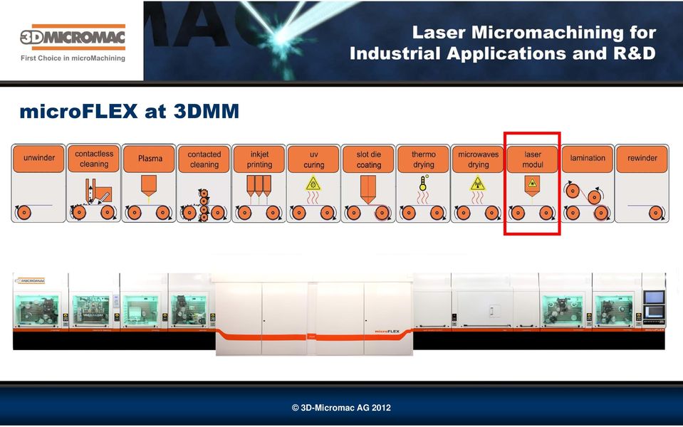
5 microflex at 3DMM
6 Laser Processing Fixed Optics

7 Laser Processing Scanner

8 Applications Laser Thin-Film Ablation Organic Photovoltaics Laser Thin-Film Ablation OLEDs Summary

9 Laser Thin-Film Ablation Organic Photovoltaics

10 Organic Photovoltaics Ag P3HT : PCBM PEDOT : PSS ITO Substrate light Organic Solar Cell conventional stack layout

11 Experimental Setup laser source beam path 2D scanner f-theta lens 2D-scanner performance parameters Repeatability < 22µrad Tracking error: 0.18 ms Long term drift < 0.6 mrad vacuum exhaust

12 Experimental Setup Laser Sources Laser Wavelength in nm Pulse duration Repetition rate in khz Average power in W Machining speed in mm/s ns laser 1064 ~ 30 ns ps laser 1064/532/355 < 12 ps fs - laser 1024/512 < 500 fs

13 ITO on Glass

14 ns Laser Wavelength λ = 1064 nm ITO layer on glass substrate: Cracks in substrate ITO layer melted ITO layer on PET foil substrate: PET foil massively damaged Huge ITO bulges at the cutting edges microscope image microscope image

15 ps Laser Wavelength λ = 1064 nm Glass substrate DEKTAK image ITO substrate ITO bulge within range of RA ITO nm No heat affected zone No melting of ITO No cracks in substrate Good edge quality Large process window microscope image -120 substrate

16 ps Laser Wavelength λ = 532 nm Glass substrate DEKTAK image ITO substrate ITO bulge within range of RA ITO nm 0-60 Almost no heat affected zone No melting of ITO No cracks in substrate Good edge quality, comparable to 1064 nm microscope image -120 substrate

17 ps Laser Wavelength λ = 355 nm Glass substrate DEKTAK image ITO substrate ITO microscope image bulge between nm ITO nm 0-60 Small heat affected zone No melting of ITO No cracks in substrate Good edge quality -120 substrate microscope image

18 fs Laser Wavelength λ = 1024 nm Glass substrate No bulge Result comparable to ps microscope image SEM microscope

19 ITO on PET Film
20 ps Laser Wavelength λ = 1064 nm PET film substrate (thickness ~50 µm) DEKTAK image microscope image nm No heat affected zone ITO bulge less than 20 nm! 40 Good edge quality substrate ITO ITO 0 Small debris in proximity to the scribed area -40 Large process window microscope image Slight delamination of ITO at the substrate -80 REM microscope cutting edge

21 ps Laser Wavelength λ = 532 nm PET film substrate (thickness ~50 µm) DEKTAK image ITO bulge nm nm 40 Small heat affected zone Average edge quality heat affected zone substrate ITO ITO 0-40 Some debris in and around machining area microscope microscope image image -80 substrate
22 ps Laser Wavelength λ = 355 nm PET film substrate (thickness ~50 µm) Heat affected zone ITO substrate Damaged substrate due to high absorption Low edge quality due to chipping of ITO microscope image
23 fs Laser Wavelength λ = 1024 nm PET-foil substrate (thickness ~50 µm) Minimal damage to PET film Smooth cutting edge No delamination of ITO layer microscope image SEM microscope
24 Conclusions to Scribing of ITO Indium tin oxide λ = 1064 nm excellent scribing quality on both glass and film λ = 532 nm λ = 355 nm good scribes on glass but shows higher bulging on film good scribes on glass but damages foil due to high absorption λ = 1064 nm is to be preferred Best scribing quality on both glass and film High output powers available Relatively inexpensive laser source available ps laser for scribing on glass substrates fs laser for scribing on polymer substrates
25 Applications Laser Thin-Film Ablation Organic Photovoltaics Laser Thin-Film Ablation OLEDs Summary
26 Laser Thin-Film Ablation OLEDs
27 OLED Layout and Scribing P1 Scribe: Isolation cut in back electrode P2 Scribe: Selective ablation of organic stack P3 Scribe: Isolation cut in front contact
28 Experimental Setup laser source beam path 2D scanner f-theta lens 2D-scanner performance parameters Repeatability < 22µrad Tracking error: 0.18 ms Long term drift < 0.6 mrad vacuum exhaust
29 Experimental Setup Laser Source Ultra-short pulse picosecond laser Pulse repetition rate up to 1 MHz Pulse duration < 12 ps Average power up to 50 W (@1064 nm) Wavelengths 1064/532/355 nm
30 P1 Scribe: ps Laser Wavelength λ = 1064 nm Ablation of back contact metal layer not possible without ablation of passivation layer optical microscopy
31 P1 Scribe: ps Laser Wavelength λ = 532 nm surface profile Markspeed mm/s Bulge < 20 nm Selective ablation of metal back contact Almost no debris generated optical microscopy
32 P1 Scribe: ps Laser Wavelength λ = 355 nm Markspeed mm/s ITO Bulge < 50 nm Selective ablation of metal back substrate electrode Smooth cutting edge surface profile optical microscopy
33 P2 Scribe: ps Laser Wavelength λ = 1064 nm Markspeed mm/s No bulge observed Good edge quality Back electrode not fully uncovered surface profile optical microscopy
34 P2 Scribe: ps Laser Wavelength λ = 532 nm Markspeed mm/s Bulge < 10 nm Good edge quality Back electrode fully uncovered surface profile optical microscopy
35 P2 Scribe: ps Laser Wavelength λ = 355 nm Markspeed mm/s Bulge < 10 nm Back electrode fully uncovered Organic stack step wise ablated at surface profile cutting edge optical microscopy
36 P3 Scribe: ps Laser Wavelength λ = 1064 nm Markspeed mm/s Bulge < 20 nm Good edge quality Stepwise ablation of multiple layers surface profile OLED stack not fully ablated optical microscopy
37 P3 Scribe: ps Laser Wavelength λ = 532 nm Markspeed mm/s Bulge < 30 nm Good edge quality OLED stack fully ablated surface profile optical microscopy
38 P3 Scribe: ps Laser Wavelength λ = 355 nm Markspeed mm/s Delamination of brittle metal layer Markspeed mm/s Generation of large bulge (~100 nm) surface profile optical microscopy
39 Conclusions to Laser Scribing of OLEDs with ps-laser P1 Scribe: ps-laser with green wavelength is recommended Maximum achievable machining speed approximately mm/s. P2 Scribe: ps-laser with green wavelength is recommended Maximum achievable machining speed approximately mm/s. P3 Scribe: ps-laser with IR or green wavelength is recommended Maximum achievable machining speed approximately mm/s.
40 Applications Laser Thin-Film Ablation Organic Photovoltaics Laser Thin-Film Ablation OLEDs Summary
41 Summary This looks quite simple, doesn t it? Several things can be learned: 1. There is a difference between the ablation from foil and glass 2. The necessary power (fluence) is usually smaller on foil than on glass And it is getting even more complicated
42 Experiment 1 Three different stacks with identical top layer Experiment with single pulses with a 1064 nm ps-laser Layer to be ablated: always 120 nm thick Fluence
43 Experiment 2 Equal stack with different top layer thicknesses In comparison the layer thickness has only few impact on the other side 120nm 240nm Fluence
44 Vielen Dank für Ihre Aufmerksamkeit! 3D-Micromac AG Technologie-Campus Chemnitz Telefon: / Fax: / info@3d-micromac.com Internet:
High power picosecond lasers enable higher efficiency solar cells.
 White Paper High power picosecond lasers enable higher efficiency solar cells. The combination of high peak power and short wavelength of the latest industrial grade Talisker laser enables higher efficiency
Laboratory #3 Guide: Optical and Electrical Properties of Transparent Conductors -- September 23, 2014
 Laboratory #3 Guide: Optical and Electrical Properties of Transparent Conductors -- September 23, 2014 Introduction Following our previous lab exercises, you now have the skills and understanding to control
Laser drilling up to15,000 holes/sec in silicon wafer for PV solar cells
 Laser drilling up to15,000 holes/sec in silicon wafer for PV solar cells Rahul Patwa* a, Hans Herfurth a, Guenther Mueller b and Khan Bui b a Fraunhofer Center for Laser Technology, 48170 Port Street,
Advanced Laser Microfabrication in High Volume Manufacturing
 Advanced Laser Microfabrication in High Volume Manufacturing IPG Photonics Microsystems Division 220 Hackett Hill Road, Manchester NH, 03102USA E-mail: jbickley@ipgphotonics.com There is increased interest
INVESTIGATION OF DIFFERENT LASER CUTTING STRATEGIES FOR SIZING OF LI-ION BATTERY ELECTRODES M804
 INVESTIGATION OF DIFFERENT LASER CUTTING STRATEGIES FOR SIZING OF LI-ION BATTERY ELECTRODES M804 Rahul Patwa 1, Hans Herfurth 1, Stefan Heinemann 1, Jyoti Mazumder 2, Dongkyoung Lee 2 1 Fraunhofer Center
histaris Inline Sputtering Systems
 vistaris histaris Inline Sputtering Systems Inline Sputtering Systems with Vertical Substrate Transport Modular System for Different Applications VISTARIS Sputtering Systems The system with the brand name
1. INTRODUCTION ABSTRACT
 MultiWave Hybrid Laser Processing of Micrometer Scale Features for Flexible Electronics Applications J. Hillman, Y. Sukhman, D. Miller, M. Oropeza and C. Risser Universal Laser Systems, 7845 E. Paradise
For Touch Panel and LCD Sputtering/PECVD/ Wet Processing
 production Systems For Touch Panel and LCD Sputtering/PECVD/ Wet Processing Pilot and Production Systems Process Solutions with over 20 Years of Know-how Process Technology at a Glance for Touch Panel,
Organic semiconductors
 Plastic (Organic) Solar Cells: Accomplishments, Challenges, and Strategies Sumit Chaudhary Assistant Professor Department of Electrical and Computer Engineering Materials Science and Engineering Iowa State
Laser Concepts for Industrial Thin Film PV Production
 Laser Concepts for Industrial Thin Film PV Production Michael Haase Nachname Carl BaaselVorname Lasertechnik GmbH & Co. KG Position Starnberg / Günding Starnberg 06. September 2006 January, 27th. - 28th.
EFFICIENT USE OF SHORT PULSE WIDTH LASER FOR MAXIMUM MATERIAL REMOVAL RATE Paper# M602
 EFFICIENT USE OF SHORT PULSE WIDTH LASER FOR MAXIMUM MATERIAL REMOVAL RATE Paper# M602 Ashwini Tamhankar and Rajesh Patel Spectra-Physics Lasers, Newport Corporation, 3635 Peterson Way, Santa Clara, CA
Laser Based Micro and Nanoscale Manufacturing and Materials Processing
 Laser Based Micro and Nanoscale Manufacturing and Materials Processing Faculty: Prof. Xianfan Xu Email: xxu@ecn.purdue.edu Phone: (765) 494-5639 http://widget.ecn.purdue.edu/~xxu Research Areas: Development
THE FUTURE OF MEDICAL MANUFACTURING LASER SOLUTIONS FOR THE MEDICAL DEVICE TECHNOLOGY
 THE FUTURE OF MEDICAL MANUFACTURING LASER SOLUTIONS FOR THE MEDICAL DEVICE TECHNOLOGY WE THINK LASER Laser Solutions for Medical Device Manufacturing When Precision Matters Most BIOPSY FORCEPS CRT LEAD
Millijoules high master-slave pulse ratio 532 nm picosecond laser
 Millijoules high master-slave pulse ratio 532 nm picosecond laser Zhao You Fan Zhongwei 1, Bai Zhenao 12, Zhang Guoxin 2, Lian Fuqiang 12, Zhao You 3, Shen Ming 3 1 Academy of Opto-Electronics, Chinese
Corning HPFS 7979, 7980, 8655 Fused Silica. Optical Materials Product Information Specialty Materials Division
 Corning HPFS 7979, 7980, 8655 Fused Silica Optical Materials Product Information Specialty Materials Division HPFS 7979, 7980 and 8655 Fused Silica HPFS Fused Silica glasses are known throughout the industry
OLED Status quo and Merck s position
 OLED Status quo and Merck s position Merck Information Day 2013 A Deep Dive into Merck s LC&OLED Business Dr. Udo Heider Vice President OLED Darmstadt, Germany June 26, 2013 Disclaimer Remarks All comparative
Real-world applications of intense light matter interaction beyond the scope of classical micromachining.
 Dr. Lukas Krainer lk@onefive.com CEO Real-world applications of intense light matter interaction beyond the scope of classical micromachining. 1 Management & Company Company Based in Zürich, Switzerland
Light management for photovoltaics. Ando Kuypers, TNO Program manager Solar
 Light management for photovoltaics Ando Kuypers, TNO Program manager Solar Global energy consumption: 500 ExaJoule/Year Solar irradiation on earth sphere: 5.000.000 ExaJoule/year 2 Capturing 0,01% covers
Prospects of Laser Polishing for Small and Complexly Shaped Parts
 Prospects of Laser Polishing for Small and Complexly Shaped Parts High Speed / High Precision Laser Microfabrication June 18, 2014 Fraunhofer Institute for Laser Technology ILT Steinbachstraße 15 52074
Laser hole drilling and texturing (for joining) of composites
 of composites") AILU Workshop: Laser processing of polymer, metal and cerramic composites Laser hole drilling and texturing (for joining) of composites Dr Paul French Photonics in Engineering Research Group General Engineering
AILU Workshop: Laser processing of polymer, metal and cerramic composites Laser hole drilling and texturing (for joining) of composites Dr Paul French Photonics in Engineering Research Group General Engineering
LASER ENGRAVING REFLECTIVE METALS TO CREATE SCANNER READABLE BARCODES Paper P516
 LASER ENGRAVING REFLECTIVE METALS TO CREATE SCANNER READABLE BARCODES Paper P516 Paul M Harrison, Jozef Wendland, Matthew Henry Powerlase Ltd, Imperial House, Link 10, Napier Way, Crawley, West Sussex,
Advancements in High Frequency, High Resolution Acoustic Micro Imaging for Thin Silicon Applications
 Advancements in High Frequency, High Resolution Acoustic Micro Imaging for Thin Silicon Applications Janet E. Semmens Sonoscan, Inc. 2149 E. Pratt Boulevard Elk Grove Village, IL 60007 USA Phone: (847)
Single Mode Fiber Lasers
 Single Mode Fiber Lasers for Industrial and Scientific Applications T h e P o w e r t o T r a n s f o r m T M IPG s Single Mode Fiber Lasers Advantages IPG's YLR-SM Series represents a break-through generation
Silicon Wafer Solar Cells
 Silicon Wafer Solar Cells Armin Aberle Solar Energy Research Institute of Singapore (SERIS) National University of Singapore (NUS) April 2009 1 1. PV Some background Photovoltaics (PV): Direct conversion
Solar Photovoltaic (PV) Cells
 Cells") Solar Photovoltaic (PV) Cells A supplement topic to: Mi ti l S Micro-optical Sensors - A MEMS for electric power generation Science of Silicon PV Cells Scientific base for solar PV electric power generation
Solar Photovoltaic (PV) Cells A supplement topic to: Mi ti l S Micro-optical Sensors - A MEMS for electric power generation Science of Silicon PV Cells Scientific base for solar PV electric power generation
Optical Hyperdoping: Transforming Semiconductor Band Structure for Solar Energy Harvesting
 Optical Hyperdoping: Transforming Semiconductor Band Structure for Solar Energy Harvesting 3G Solar Technologies Multidisciplinary Workshop MRS Spring Meeting San Francisco, CA, 5 April 2010 Michael P.
Results Overview Wafer Edge Film Removal using Laser
 Results Overview Wafer Edge Film Removal using Laser LEC- 300: Laser Edge Cleaning Process Apex Beam Top Beam Exhaust Flow Top Beam Scanning Top & Top Bevel Apex Beam Scanning Top Bevel, Apex, & Bo+om
Zero Width Glass Cutting with CO 2 Laser
 Zero Width Glass Cutting with CO 2 Laser Mohammed Naeem GSI Group, Laser Division Cosford Lane, Swift Valley Rugby mnaeem@gsig.com Introduction Laser cutting of glass in not a novel technique, excellent
Development of certified reference material of thin film for thermal diffusivity
 Development of certified reference material of thin film for thermal diffusivity Takashi Yagi, Thermophysical properties section, NMIJ/AIST Joshua Martin MML, National Institute of Standards and Technology
Pulsed laser deposition of organic materials
 Pulsed laser deposition of organic materials PhD theses Gabriella Kecskeméti Department of Optics and Quantum Electronics University of Szeged Supervisor: Dr. Béla Hopp senior research fellow Department
FRAUNHOFER IPMS: WE SHAPE THE LIGHT. PRODUCTS AND FIELDS OF APPLICATION
 FRAUNHOFER IPMS: WE SHAPE THE LIGHT. PRODUCTS AND FIELDS OF APPLICATION DR. HARALD SCHENK 10.03.2010 AGENDA Fraunhofer- Gesellschaft Fraunhofer-IPMS in Profile Products and Fields of Application AGENDA
Microstructuring of resist double layers by a femtosecond laser ablation and UV lithography hybrid process
 Microstructuring of resist double layers by a femtosecond laser ablation and UV lithography hybrid process Tamara Pacher 1, Adrian Prinz 2, Stefan Partel 1, Sandra Stroj 1 1 Josef-Ressel-Center for material
SpeedLight 2D. for efficient production of printed circuit boards
 laser direct imaging SpeedLight 2D laser direct imaging platform for efficient production of printed circuit boards MANZ AG /// Manz SpeedLight 2D /// 2 History of the development of Manz SpeedLight 2D
Reactive Fusion Cutting When gas used reacts with gas (usually oxygen) burn reaction adds energy to effect Steel typically 60% added energy Titanium
 burn reaction adds energy to effect Steel typically 60% added energy Titanium") Reactive Fusion Cutting When gas used reacts with gas (usually oxygen) burn reaction adds energy to effect Steel typically 60% added energy Titanium 90% added energy However can reaction can chemically
Reactive Fusion Cutting When gas used reacts with gas (usually oxygen) burn reaction adds energy to effect Steel typically 60% added energy Titanium 90% added energy However can reaction can chemically
ADVANCED DIRECT IMAGING. by ALTIX
 ADVANCED DIRECT IMAGING by ALTIX ADVANCED DIRECT IMAGING by ALTIX No need for phototools and films preparation processes ALDS Advanced high power Leds with high resolution DMD System Fully Intuitive Human
OLED - Technologie der Zukunft
 OLED - Technologie der Zukunft Dr. Manfred Weigand MERCK KGaA, Darmstadt, Germany Cleanzone 2014 Cathode Ray Tube (CRT) Source: Peter Littmann Source: Patrick Schindler Source: Bundesarchiv, Bild 183-H0812-0031-001
Major LED manufacturing trends and challenges to support the general lighting application
 Major LED manufacturing trends and challenges to support the general lighting application Semicon Russia 2011, June 1st! Ralph Zoberbier Director Product Management Aligner Content" 1. SUSS MicroTec Introduction
T.M.M. TEKNIKER MICROMACHINING
 T.M.M. TEKNIKER MICROMACHINING Micro and Nanotechnology Dapartment FUNDACION TEKNIKER Avda. Otaola. 20 Tel. +34 943 206744 Fax. +34 943 202757 20600 Eibar http://www.tekniker.es TMM FACILITIES -Clean Room
Holographically corrected microscope with a large working distance (as appears in Applied Optics, Vol. 37, No. 10, 1849-1853, 1 April 1998)
") Holographically corrected microscope with a large working distance (as appears in Applied Optics, Vol. 37, No. 10, 1849-1853, 1 April 1998) Geoff Andersen and R. J. Knize Laser and Optics Research Center
Holographically corrected microscope with a large working distance (as appears in Applied Optics, Vol. 37, No. 10, 1849-1853, 1 April 1998) Geoff Andersen and R. J. Knize Laser and Optics Research Center
Neuere Entwicklungen zur Herstellung optischer Schichten durch reaktive. Wolfgang Hentsch, Dr. Reinhard Fendler. FHR Anlagenbau GmbH
 Neuere Entwicklungen zur Herstellung optischer Schichten durch reaktive Sputtertechnologien Wolfgang Hentsch, Dr. Reinhard Fendler FHR Anlagenbau GmbH Germany Contents: 1. FHR Anlagenbau GmbH in Brief
Innovative Wafer and Interconnect Technologies - Enabling High Volume Low Cost RFID Solutions
 Innovative Wafer and Interconnect Technologies - Enabling High Volume Low Cost RFID Solutions Innovative Wafer & Interconnect Technologies Outline Low cost RFID Tags & Labels Standard applications and
Faszination Licht. Entwicklungstrends im LED Packaging. Dr. Rafael Jordan Business Development Team. Dr. Rafael Jordan, Business Development Team
 Faszination Licht Entwicklungstrends im LED Packaging Dr. Rafael Jordan Business Development Team Agenda Introduction Hermetic Packaging Large Panel Packaging Failure Analysis Agenda Introduction Hermetic
Acoustic GHz-Microscopy: Potential, Challenges and Applications
 Acoustic GHz-Microscopy: Potential, Challenges and Applications A Joint Development of PVA TePLa Analytical Systems GmbH and Fraunhofer IWM-Halle Dr. Sebastian Brand (Ph.D.) Fraunhofer CAM Fraunhofer Institute
Crystallization of Amorphous Silicon Using Xenon Flash Lamp Annealing
 Crystallization of Amorphous Silicon Using Xenon Flash Lamp Annealing Henry Hellbusch 2/5/2016 RIT - Corning - Crystallization of A-Si with FLA 1 Purpose Thin Film Transistors (TFT) on glass are utilized
Flexible Mehrlagen-Schaltungen in Dünnschichttechnik:
 Flexible Mehrlagen-Schaltungen in Dünnschichttechnik: Technologie-Plattform für Intelligente Implantate A. Kaiser, S. Löffler, K. Rueß, P. Matej, C. Herbort, B. Holl, G. Bauböck Cicor Advanced Microelectronics
TruMicro: Power meets precision. Machine tools / Power tools Laser technology / Electronics
 TruMicro: Power meets precision. Machine tools / Power tools Laser technology / Electronics Great results on a small scale. Contents Great results on a small scale. 2 Cold material processing. 4 Our expertise
ADVANCED LAER TECHNOLOGY
 Since 1999 www.kortherm.co.kr ADVANCED LAER TECHNOLOGY Advanced Laserr Technology at KORTherm Science S Since founded in 1999 we put our endeavor intto building a specialized business, focusing on the
Femtosecond laser-induced silicon surface morphology in water confinement
 Microsyst Technol (2009) 15:1045 1049 DOI 10.1007/s00542-009-0880-8 TECHNICAL PAPER Femtosecond laser-induced silicon surface morphology in water confinement Yukun Han Æ Cheng-Hsiang Lin Æ Hai Xiao Æ Hai-Lung
REPAIR CONCEPT SUPPORTED BY LASER REMOVAL AND INDUCTIVE HEATING
 28 TH INTERNATIONAL CONGRESS OF THE AERONAUTICAL SCIENCES REPAIR CONCEPT SUPPORTED BY LASER REMOVAL AND INDUCTIVE HEATING Markus Kaden*, Rüdiger Keck* *German Aerospace Center markus.kaden@dlr.de;ruediger.keck@dlr.de
Quasi-Continuous Wave (CW) UV Laser Xcyte Series
 UV Laser Xcyte Series") COMMERCIAL LASERS Quasi-Continuous Wave (CW) UV Laser Xcyte Series Key Features 355 nm outputs available Quasi-CW UV output Field-proven Direct-Coupled Pump (DCP ) TEM00 mode quality Light-regulated output
COMMERCIAL LASERS Quasi-Continuous Wave (CW) UV Laser Xcyte Series Key Features 355 nm outputs available Quasi-CW UV output Field-proven Direct-Coupled Pump (DCP ) TEM00 mode quality Light-regulated output
FOR HIGH-TECH PRODUCTION
 AUTOMATION & METROLOGY AUTOMATION & METROLOGY SOLUTIONS FOR HIGH-TECH PRODUCTION key technologies for multiple industries MANZ AG /// hightech solutions /// 5 2015 Acquisition of KLEO, a company of the
Femtosecond Laser Micromachining
 Femtosecond Laser Micromachining 02/03/2010 Spring 2010 MSE503 Seminar Deepak Rajput Center for Laser Applications University of Tennessee Space Institute Tullahoma, Tennessee 37388-9700 Email: drajput@utsi.edu
Design qualification and type approval of PV modules
 Design qualification and type approval of PV modules TÜV Immissionsschutz und Energiesysteme GmbH Test Centre for Energy technologies May 2003 Design qualification and type approval of PV-modules in accordance
Pump-probe experiments with ultra-short temporal resolution
 Pump-probe experiments with ultra-short temporal resolution PhD candidate: Ferrante Carino Advisor:Tullio Scopigno Università di Roma ƒla Sapienza 22 February 2012 1 Pump-probe experiments: generalities
F ormation of Very Low Resistance Contact for Silicon Photovoltaic Cells. Baomin Xu, Scott Limb, Alexandra Rodkin, Eric Shrader, and Sean Gamer
 F ormation of Very Low Resistance Contact for Silicon Photovoltaic Cells Baomin Xu, Scott Limb, Alexandra Rodkin, Eric Shrader, and Sean Gamer Palo Alto Research Center, 3333 Coyote Hill Road, Palo Alto,
Time resolved study of femtosecond laser induced micromodifications inside transparent brittle materials
 9th International Conference on Photonic Technologies LANE 2016 Time resolved study of femtosecond laser induced micromodifications inside transparent brittle materials F. Hendricks a, *, V.V. Matylitsky
Get PCB Prototypes Sooner with In-House Rapid PCB Prototyping
 Get PCB Prototypes Sooner with In-House Rapid PCB Prototyping Save Time with In-House Prototyping In-house circuit board prototyping eliminates waiting for external suppliers. With LPKF systems and solutions,
Overview of Optical Recording Technology- Current Status and Near Term Projections
 Overview of Optical Recording Technology- Current Status and Near Term Projections Koichi Sadashige Sadashige Associates 15 Amherst Rd, Voorhees NJ 08043-4901 Phone: +1-856-767-2644, FAX: +1-856-767-1462
FAST and CURIOUS A brief introduction to ultrafast lasers and their applications
 FAST and CURIOUS A brief introduction to ultrafast lasers and their applications Dr. Maria Ana Cataluna m.a.cataluna@dundee.ac.uk School of Engineering, Physics and Mathematics University of Dundee How
MicroScan. Excimer laser system for all types of vision corrections OPTOSYSTEMS LTD.
 MicroScan Excimer laser system for all types of vision corrections OPTOSYSTEMS LTD. МicroScan is a new generation excimer laser system for all types of vision corrections: myopia, hypermetropia, astigmatism.
Any Material - Any Process Superior Reliability & Performance
 Lasers for Materials Processing Any Material - Any Process Superior Reliability & Performance Delivering the Right Las er for Your Application Materials processing experts today face a wide range of choices
Exploring the deposition of oxides on silicon for photovoltaic cells by pulsed laser deposition
 Applied Surface Science 186 2002) 453±457 Exploring the deposition of oxides on silicon for photovoltaic cells by pulsed laser deposition Lianne M. Doeswijk a,*, Hugo H.C. de Moor b, Horst Rogalla a, Dave
Description and Investigation of Size Effects in the Scaling of a Hot Forging Process into the Microscale
 Description and Investigation of Size Effects in the Scaling of a Hot Forging Process into the Microscale J.P. Wulfsberg 1, M. Terzi 1 1 Laboratory of Production Engineering, Helmut-Schmidt-University
Applied Surface Science 8118 (2002) 1 5
 1 5") 3 Radioactive oxide removal by XeCl laser 4 Ph. Delaporte a,*, M. Gastaud a, W. Marine b, M. Sentis a, O. Uteza a, 5 P. Thouvenot c, J.L. Alcaraz c, J.M. Le Samedy c, D. Blin d 6 a Lasers, Plasmas and
3 Radioactive oxide removal by XeCl laser 4 Ph. Delaporte a,*, M. Gastaud a, W. Marine b, M. Sentis a, O. Uteza a, 5 P. Thouvenot c, J.L. Alcaraz c, J.M. Le Samedy c, D. Blin d 6 a Lasers, Plasmas and
Ultimate code quality on a wide variety of substrates. Coding and marking sample guide. CO2 Laser
 Ultimate code quality on a wide variety of substrates Coding and marking sample guide CO2 Laser Achieving the best laser mark is all about the specification process. Laser marking systems can generate
Scanning Near Field Optical Microscopy: Principle, Instrumentation and Applications
 Scanning Near Field Optical Microscopy: Principle, Instrumentation and Applications Saulius Marcinkevičius Optics, ICT, KTH 1 Outline Optical near field. Principle of scanning near field optical microscope
Light management for photovoltaics using surface nanostructures
 Light management for photovoltaics using surface nanostructures Roberta De Angelis Department of Industrial Engineering and INSTM, University of Rome Tor Vergata New Materials For Optoelectronics webnemo.uniroma2.it
High Power Fiber Laser Technology
 High Power Fiber Laser Technology Bill Shiner VP Industrial September 10, 2013 IDOE LSO Workshop Global Production Facilities Production Facilities and World Headquarters Oxford, Massachusetts Production
Investigation of the Optical Properties of Liquid Deposition CuSO 4 Thin Film
 015 IJSRST Volume 1 Issue 5 Print ISSN: 395-6011 Online ISSN: 395-60X Themed Section: Science and Technology Investigation of the Optical Properties of Liquid Deposition CuSO 4 Thin Film Nafie A. Almuslet
METHODS FOR PULSED LASER DEPOSITION OF LARGE-AREA FILMS USING MORE THAN ONE TARGET
 Laser Physics 0 International Journal of Modern Physics: Conference Series Vol. 5 (0) 70 78 World Scientific Publishing Company DOI: 0.4/S009450078 METHODS FOR PULSED LASER DEPOSITION OF LARGE-AREA FILMS
Optical coherence tomography as a tool for non destructive quality control of multi-layered foils
 Optical coherence tomography as a tool for non destructive quality control of multi-layered foils Günther Hannesschläger, Alexandra Nemeth, Christian Hofer, Christian Goetzloff, Jens Reussner, Karin Wiesauer,
Michalina Góra, Jan Marczak, Antoni Rycyk, Piotr Targowski APPLICATION OF OPTICAL COHERENCE TOMOGRAPHY TO MONITORING OF LASER ABLATION OF VARNISH
 Michalina Góra, Jan Marczak, Antoni Rycyk, Piotr Targowski APPLICATION OF OPTICAL COHERENCE TOMOGRAPHY TO MONITORING OF LASER ABLATION OF VARNISH Institute of Physics, Nicolaus Copernicus University, Toruń,
PCB Laser Technology for Rigid and Flex HDI Via Formation, Structuring, Routing
 Abstract PCB Laser Technology for Rigid and Flex HDI Via Formation, Structuring, Routing Dr. Dieter J. Meier, Stephan H. Schmidt* LPKF Laser & Electronics AG Garbsen, Germany and Wilsonville, OR* A new
Materials for Organic Electronic. Jeremy Burroughes FRS FREng
 Materials for Organic Electronic Applications Jeremy Burroughes FRS FREng Introduction Organic Thin Film Transistors Organic Solar Cells and Photodiodes All Printed OLED Summary 4k2k 56 Displays Panasonic
Ultrahigh-efficiency solar cells based on nanophotonic design
 Ultrahigh-efficiency solar cells based on nanophotonic design Albert Polman Piero Spinelli Jorik van de Groep Claire van Lare Bonna Newman Erik Garnett Marc Verschuuren Ruud Schropp Wim Sinke Center for
Coating Thickness and Composition Analysis by Micro-EDXRF
 Application Note: XRF Coating Thickness and Composition Analysis by Micro-EDXRF www.edax.com Coating Thickness and Composition Analysis by Micro-EDXRF Introduction: The use of coatings in the modern manufacturing
UV-NIR LASER BEAM PROFILER
 CinCam CMOS - Technical Data - CMOS-1201 CMOS-1202 CMOS-1203 CMOS-1204 Standard Series Standard Series Standard Series Standard Series SENSOR DATA Format: 1/2 1/1.8 1/1.8 1/2.5 Active area (without cover
Mass production, R&D Failure analysis. Fault site pin-pointing (EM, OBIRCH, FIB, etc. ) Bottleneck Physical science analysis (SEM, TEM, Auger, etc.
 Bottleneck Physical science analysis (SEM, TEM, Auger, etc.") Failure Analysis System for Submicron Semiconductor Devices 68 Failure Analysis System for Submicron Semiconductor Devices Munetoshi Fukui Yasuhiro Mitsui, Ph. D. Yasuhiko Nara Fumiko Yano, Ph. D. Takashi
Failure Analysis System for Submicron Semiconductor Devices 68 Failure Analysis System for Submicron Semiconductor Devices Munetoshi Fukui Yasuhiro Mitsui, Ph. D. Yasuhiko Nara Fumiko Yano, Ph. D. Takashi
Analysis of Blind Microvias Forming Process in Multilayer Printed Circuit Boards
 POLAND XXXII International Conference of IMAPS - CPMT IEEE Poland Pułtusk - 4 September 008 Analysis of Blind Microvias Forming Process in Multilayer Printed Circuit Boards Janusz Borecki ), Jan Felba
film stretching production lines and components Specialty Machinery Quality creates value MF 1
 film stretching production lines and components Quality creates value Specialty Machinery MF 1 Film stretching Lines and Equipment Film Stretching lines ahead of standard with custom-made systems Sheets
Figure 1 Wafer with Notch
 Glass Wafer 2 SCHOTT is an international technology group with more than 125 years of experience in the areas of specialty glasses, materials and advanced technologies. With our high-quality products and
DIODE PUMPED CRYSTALASER
 DIODE PUMPED CRYSTALASER Ultra-compact CW & Pulsed Turnkey Systems UV Visible to IR High Reliability High Stability High Efficiency TEMoo & SLM Low Noise Low Cost ULTRA-COMPACT DIODE-PUMPED CRYSTAL LASER
Laser beam sintering of coatings and structures
 Laser beam sintering of coatings and structures Anne- Maria Reinecke, Peter Regenfuß, Maren Nieher, Sascha Klötzer, Robby Ebert, Horst Exner Laserinstitut Mittelsachsen e.v. an der Hochschule Mittweida,
Design and Test of Fast Laser Driver Circuits
 Design and Test of Fast Laser Driver Circuits Since the invention of the laser by Theodore H Maiman 50 years ago, lasers have found widespread applications in various technological fields, such as telecommunications,
HIGH POWER FREE SPACE AND FIBER PIGTAILED ISOLATORS
 NEW HIGH POWER FREE SPACE AND FIBER PIGTAILED ISOLATORS Features: New! Reduced size and cost versions Reliable high power handling: As much as 80 Watts High Isolation, up to 50dB isolation possible from
ROFIN FL SERIES. High Brightness Fiber Lasers Precise, Fast and Reliable.
 LASER MACRO ROFIN FL SERIES High Brightness Fiber Lasers Precise, Fast and Reliable. T H E P O W E R O F L I G H T ROFIN FL SERIES THE PRODUCT Ideal Beam Quality for Every Application The high brightness
Applications. Blue IF 039, Green IF 062, Yellow IF 022, Orange IF 041, Red IF 090,Dark Red IF 091 IR pass IF 092, IF098, IF 093 Surface 1 5/2 0.
 Color Filters Blue, Green, Yellow, Orange, Red & NIR Color Filters Blue and Green filters, transmitts wavelength in a corresponding color as seen by the human eye, while yellow, orange and red are long
Nanotribology of Hard Thin Film Coatings: A Case Study Using the G200 Nanoindenter
 Nanotribology of Hard Thin Film Coatings: A Case Study Using the G200 Nanoindenter Application Note Introduction Thin film coatings are extensively used in various applications, such as microelectronics,
F L E X F L E X. Each year worldwide flex circuit demand increases, due primarily LA S E R PRO C E S S I N G O F. Polyimide requires special methods,
 Polyimide requires special methods, LA S E R PRO C E S S I N G O F F L E X F L E X BY SRI VENKAT Each year worldwide flex circuit demand increases, due primarily to the advantages flex offers in space
Designing and Manufacturing Femtoseconds Ultra-broadband Lasers: Proven, Hands-free Reliability
 Technical Note Designing and Manufacturing Femtoseconds Ultra-broadband Lasers: Proven, Hands-free Reliability This whitepaper reviews how design choices, manufacturing steps and testing protocols substantially
ASI OEM Outdoor Solar Modules
 SOLAR PHOTOVOLTAICS ASI OEM OUTDOOR E ASI OEM Outdoor Solar Modules for innovative autarchic electronic devices More Energy Double-stacked cells Stable performance Reliability and Quality Made in Germany
Why Using Laser for Dust Removal from Tokamaks
 1 FTP/P1-25 Why Using Laser for Dust Removal from Tokamaks Ph. Delaporte 1), A. Vatry 1), 2), D. Grojo 1), M. Sentis 1), C. Grisolia 2) 1) Laboratoire Lasers, Plasmas et Procédés Photoniques, campus de
OLED display. Ying Cao
 OLED display Ying Cao Outline OLED basics OLED display A novel method of fabrication of flexible OLED display Potentials of OLED Suitable for thin, lightweight, printable displays Broad color range Good
Reactive Mesogens. Brighter, Clearer Communication
 Reactive Mesogens Brighter, Clearer Communication Statement Merck is the world leader in manufacturing and marketing liquid crystals (LCs). The anisotropic optical behaviour of LCs is the fundamental underlying
Micro-machining with ultrashort laser pulses: From basic understanding to technical applications
 Micro-machining with ultrashort laser pulses: From basic understanding to technical applications Friedrich Dausinger a, Helmut Hügel a, Vitali Konov b a Stuttgart University, Institut für Strahlwerkzeuge
Precision Work on the Human Eye
 Precision Work on the Human Eye Piezo-Based Nanopositioning Systems for Ophthalmology Page 1 of 5 Introduction Human beings are visual animals, in other words, they acquire most information visually. It
Thin Is In, But Not Too Thin!
 Thin Is In, But Not Too Thin! K.V. Ravi Crystal Solar, Inc. Abstract The trade-off between thick (~170 microns) silicon-based PV and thin (a few microns) film non-silicon and amorphous silicon PV is addressed
Nordson EFD Solutions: Fluid Positioning & Precision Dispensing in Mobile Device and Wearables Manufacturing
 Nordson EFD Solutions: Fluid Positioning & Precision Dispensing in Mobile Device and Wearables Manufacturing Introduction As consumers demand thinner, lighter, more sophisticated and durable mobile devices
Design qualification and type approval of PV modules acc. to IEC 61215:2005 / IEC 61646:2008
 Design qualification and type approval of PV modules acc. to IEC 61215:2005 / IEC 61646:2008 TÜV Rheinland Immissionsschutz und Energiesysteme GmbH Renewable Energies 2009-01-22 January 2009 Design qualification