EM 437 COMMUNICATION SYSTEMS II LABORATORY MANUAL FALL
|
|
|
- Bernice Montgomery
- 7 years ago
- Views:
Transcription
1 EM 437 COMMUNICATION SYSTEMS II LABORATORY MANUAL FALL

2 TABLE OF CONTENTS page LABORATORY RULES...3 CHAPTER 1: PULSE CODE MODULATION Introduction The Apparatus The Modulation Process Quantising Noise References...8 CHAPTER 2: SAMPLING AND TIME DIVISION MULTIPLEX Introduction The Apparatus The Sampling Process-Theory Time Division Multiplexing Observation of Signals References...15 Appendix 1. Convolution...16 EXPERIMENT 1 : PCM CODING...17 EXPERIMENT 2 : PCM QUANTISING LEVELS...20 EXPERIMENT 3 : PCM QUANTISING NOISE...22 EXPERIMENT 4: SAMPLING AND TIME DIVISION MULTIPLEX

3 Gazi University Department of Electrical and Electronics Engineering EM437 Communication Systems II Lab. LABORATORY RULES Everyone should attend experiments on the determined days and hours. If one does not attend more than one experiment he/she will take the grade DY. There will be four experiments. Reports should include: Name and number of writer Name, purpose, theory and the procedure of experiment Comments of writer There will be a quiz for every experiment. Grading will be as follows: Experiments : 25% Quiz : 25% Performance : 10% Final Examination : 40% 3

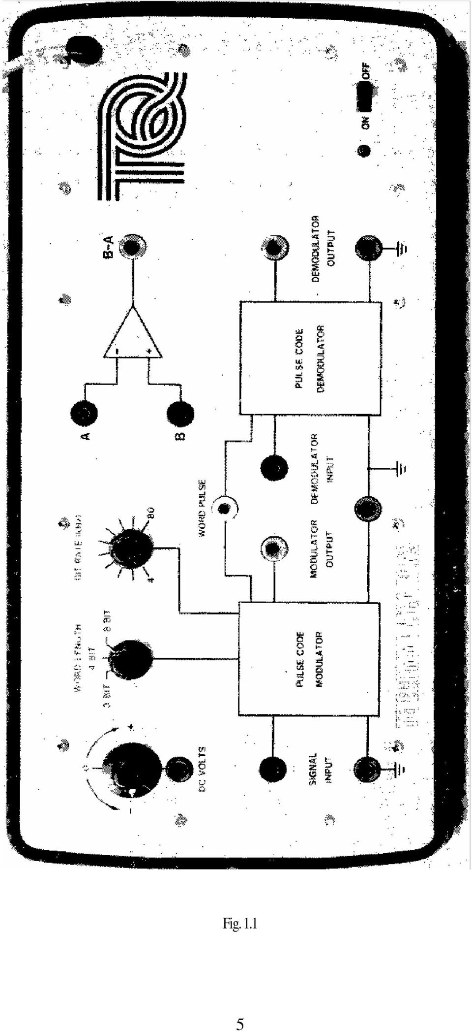
4 CHAPTER 1: PULSE CODE MODULATION Introduction Pulse Code Modulation(PCM) is by far the most important digital modulation method. It is used extensively in data and communication channels and is widely used for transmission of telephony between exchanges. In fact the words analogue-to-digital conversion (A/D) often imply PCM although other A/D methods such as delta modulation are possible. In PCM the analogue signal is first sampled and the amplitude of each sample is used to encode a stream of pulses. The coding used is often binary because binary electronic devices are cheap The Apparatus Fig.1.1 shows the apparatus, which comprises a pulse code modulator and demodulator. The input to the modulator can have a signal of any waveform or amplitude applied to it, and a separate d.c. level control is supplied on the equipment. A choice of 3,4 or 8 bit encoding is available at the modulator. The signal can be reconstituted by the pulse code demodulator. A difference amplifier is also supplied to allow the signal into the p.c.m modulator to be compared with the signal out of the p.c.m demodulator in order to establish the loss of information(i.e. added noise) as a function of the encoding, frequency and amplitude of the input signal. The following additional apparatus is required: (a) Audio Signal Generator (b) Oscilloscope The Modulation Process The signal to be transmitted is first sampled. As demonstrated in the experiment E15g(Sampling and Time Division Multiplex), the sampling rate should be at least twice the highest frequency in the waveform, otherwise aliasing distortion will occur. Each sample is then encoded into an m-bit binary word. The choice of the number of bits per word(m) is rather important and as usual there is a conflict between opposing considerations. On the one hand m bits means that there can only be 2 m possible codes to described the sample amplitude. On the other hand large values of a m mean that a higher bit rate is needed to transmit the required number of samples per second. Thus the system design requires that the minimum value of m be chosen which is consistent with adequate the signal with an m bit code. If m is chosen to be 3 then there 8 possible amplitude levels, thus, Code Level

5 Fig
6 A 3-bit code means therefore that signal only be described by 8 voltages. This may be demonstrated on the apparatus using the d.c. supply provided. This should be connected to the signal input and the code at the modulator output can be observed on the oscilloscope. It is necessary to identify the beginning of a code word and this is achieved by simultaneously displaying the word pulse. The decoded d.c voltage levels can be observed at the demodulator output after connecting the demodulator to the modulator. In this way the voltage levels for each of the 8 possibilities can be established. The experiment should be repeated for a 4-bit code with its 16 possibilities, and an 8 bit code with its 256 possibilities Quantising Noise When a 3-bit word is being used there are only 8 possible amplitudes that can be transmitted and there is therefore an error between the actual level of the signal and the transmitted signal. The process of making the amplitudes of the samples correspond to discrete levels is termed quantising and the amplitude errors introduced constitute quantising noise. Fig.1.2 shows an analogue signal and its quantised version. The error signal, also shown, is the quantised signal subtracted from the analogue signal. If the voltage difference between the quantising levels is s then the error signal is a sawtoothlike waveform of peak-to-peak amplitude s. the mean square value of such a waveform is s 2 /12 and so this quantifies the noise in PCM systems. The fact that this noise waveform contains very high frequencies does not affect the amount of noise falling into the signal board because of the sampling process. Now we have to decide what the value of s is. Suppose that level 0 in a 3-bit system is V c volts and level 7 is +V c volts then the value of s is 2 V c /7, or in general s= 2 V c / (2 m -1). (1.1) Signal S Quantised signal S Error signal Fig

7 The quantising noise N Q is thus given by : 2 2 s 4V c N Q =.. (1.2) 2m 12 12x 2 +Vc -Vc A B C The signal to noise ratio obviously depends also on the amplitude of the signal. Fig 1.3 shows the quantising levels for a 3-bit code with waveforms of 3 different amplitudes. Waveform A does not use the whole of the amplitudes available and is, therefore, unnecessarily small. Waveform C is too large because it spends a significant time out of the range of the quantising levels and therefore becomes severely clipped. Waveform B is just right. For a sine wave, therefore, it is easy to decide that the amplitude should be V c. the mean square value (s) of the sine wave is V c /2 and so the signal to quantising noise ratio becomes: s N Q 3 2m x = 2. (1.3) 2 The signal to noise ratio for various values of m are shown as follows (note the approximation in equation 1.2 causes errors for low values of m): m S/N Q (db)

8 For signals with noise-like characteristics the problem is more difficult because it is not so easy to decide what the optimum amplitude should be. For speech signals there is the additional problem that some people talk loudly and others talk more quietly. Often the quantising grids are unevenly spaced giving a process called companding and this more nearly matches the quantising grid to the statistics of the signal. The quantising of a sinusoidal signal can be observed by applying a signal of 100 Hz to the signal input and adjusting the oscilloscope for stable triggering. The modulator output can be seen to be cyclically reading through the code alphabet. By connecting the modulator output to the demodulator input and observing the demodulator output, the quantising effect of the pulse code modulation process can be clearly seen. The amplitude of the signal should now be increased so that it exceeds the extreme levels as determined by the d.c. test. Clipping of the sinusoidal signal can now be observed, high amplitudes leading to longer times during which the sinusoid is clipped. Applying a sinusoidal signal to both the signal input to terminal B of the difference amplifier, and connecting the demodulator output to terminal A, allows the quantising noise to be examined. The observed shapes should be explained as the amplitude, bits per word, bit rate and input signal frequency are varied. If an r.m.s. meter is available it can be used to measure the quantising noise power and the signal input power. This measurement can be made for various input amplitudes and a graph plotted of signal to noise ratio versus input amplitude. As explained above this should peak when the signal amplitude is near V c and the signal to noise ratio is then given by equation References 1. P.B. Johns T.R. Rowbotham, Communications Systems Analysis, Butterworth J.A. Betts, Signal Processing, Modulation and Noise, English Universities

9 CHAPTER 2: SAMPLING AND TIME DIVISION MULTIPLEX Introduction In all telecommunications networks there is a need to interconnect switching centers and telephone exchanges as economically as possible. Usually the volume of traffic over these routes makes it attractive to transmit as much information as possible over each cable. Clearly if the distance between transmitter and receiver is short the cost of the terminal equipment which combines information channels may exceed the cost of the installing extra cable pairs, thus there are certain distances below which limits can be set on the number of telephone channels it is worthwhile to combine for the purposes of transmission. Although it might appear that the economist could draw a continuous curve relating distance to the number of telephone channels, it must also be borne in mind that it is more economic to develop and manufacture a small range of products rather than a large, flexible range. Channel combining (multiplexing) equipment operating in the frequency domain is known as frequency division multiplexing(f.d.m) while in the time domain it is known as time division multiplexing(t.d.m). The quantum of telephone channels in F.D.M. is the group, which comprises twelve telephone channels, and that for T.D.M. is either twenty-four or thirty telephone channels. The common European standard has now been agreed as thirty channels, which corresponds to 2048 kbit/s. Further agreed orders in the hierarchy are at information rates of 8448 kbit/s, kbit per second and kbit per second. The basic processes in building this hierarchy from an analog telephone channel occupying 300Hz to 3400Hz are sampling at 8kHz, 8-bit encoding(as described in the pulse code modulation experiment), and time division multiplexing of 30 of these 64 kbit/s channels. This experiment investigates the first and last of these processes The Apparatus The apparatus is shown in fig.2.1. It comprises a sampling source, which may varied in frequency or sample pulse width, a multiplexer and a demultiplexer. The multiplexer accepts two or four input channels, samples each, and interleaves the samples. The signal on one of these channels is a waveform containing approximately the first and third harmonics of a 1kHz signal. The output from the multiplexer may be observed, or may be transmitted into the demultiplexer which separates the two channels, and passes the pulse train of each through a low pass filter to reconstitute the original signals. An oscilloscope and an audio signal generator are required in addition to the apparatus The Sampling Process-Theory In certain communication processes, such as pulse code modulation system described in Chapter 1, it is necessary to sample a waveform at regular intervals in order to communicate discrete information rather than continuous information. The process of sampling is equivalent to multiplying the waveform to be sampled by a series of regularly spaced delta functions as shown in fig.2.2. Such a series of delta pulses is termed the sampling function which has the interesting property that an infinite series of delta pulses in the time domain has a spectrum which is also an infinite delta series in the frequency domain. Communications engineers often have to work simultaneously in both the frequency and the time domain, and probably the best known rule which connects manipulations in these two domains is that a multiplication of waveforms in the time domain transforms in the convolution of their corresponding amplitude spectra in the frequency domain. Convolution may sound as if it s a difficult process, and indeed may be so mathematically, but it is in fact a simple geometrical process which is described in more detail in the appendix to this chapter. Thus if sampling the multiplication of the analog waveform by a delta series in the time domain, the spectrum of the sample signal is the convolution of the analog waveform spectrum with another delta series. This is shown in fig

10 Fig

11 t (a)waveform t (b) Sampling function t ( c ) = ( a ) x ( b ) Fig
 x ( b ) Fig.")
12 -fm fm f f 1/T fm f Fig. 2.3 If T is the interval between pulses in the time domain, i.e. in fig.2.2, then the corresponding interval between the frequencies which contain signal energy is 1/T. Consider an analog waveform which has a spectrum which extends from zero Hz to an upper limit of f m Hz. It can now be seen that provided 1/T is greater than 2f m then a complete replica of the spectrum of the sampled signal lies below the frequency 1/2T and the introduction of a low pass filter would restore the original signal unchanged. If, however, the frequency 1/T is less than 2f m then overlap of the spectra of the sampled signal will occur resulting in distortion. This mechanism of distortion is sometimes referred to as aliasing and is shown in fig.2.4. The preceding argument holds true even if the analog signal spectrum begins at a frequency above zero Hz, and indeed in the limit it could be a sinusoid with energy only at frequency f m. In general, therefore, if a waveform has frequencies in its spectrum extending from a lower frequency limit to an upper frequency limit f m Hz it is possible to convey all the information in that waveform by 2f m or more equally spaced samples per second of the amplitude of the waveform. This rate is often referred to as the Nyquist sampling rate. 12

13 -fm fm f f 1/T fm f Fig.2.4 In practice, an analog signal is sampled with pulses which have a nonzero width. The way in which the pulse width affects the spectrum will be used to demonstrate the effect in practice. Thinking geometrically again, a series of a broad samples is a delta series convolved with a single broad pulse. Using x for the multiplication process and * for the convolution process, fig.2.5(a) shows the procedure in constructing the practical sampled waveform. Using the rule referred to before where x and * change places when moving between time and frequency domains, fig. 2.5(b) shows how the practical spectrum is constructed. The extra ingredient used in moving from fig. 2.5(a) to fig.2.5(b) is the relationship between a square pulse and its amplitude density spectrum. This is shown in fig.2.6 which also shows that the narrower the pulse the broader the amplitude density spectrum between its central zero crossing points. In the limit of a zero width(delta) pulse this amplitude density spectrum is flat, which, when multiplied by any other spectrum, does not alter its shape, as is excepted. (a) t x t t * = t (b) * x = f f f f Fig
 shows the procedure in constructing the practical sampled waveform. Using the rule referred to before where x and * change places when moving between time and frequency domains, fig. 2.")
14 τ 1 / τ Fig Time Division Multiplexing Time division multiplexing is the process whereby two or more digital streams are combined to facilitate transmission over a common highway. Essentially the process is very simple. If 30 channels, each of 64 kbit/s are to be combined, the width of each pulse is constrained to somewhat less than 1/30 th of the tributary sampling interval which is 1/64 kbit/s. Each of the tributaries is then delayed by a multiple of 1/30 th of this interval so that when the digit streams are combined the aggregate digit rate has been substantially increased. It might be supposed that this aggregate digit rate is exactly 30x64 kbit per second, but extra digits must be added to provide ancillary functions, for example at the receiver channel identification is necessary and signaling information associated with each channel must be transmitted Observation of Signals For all the following experiments the 2/4 channel switch should be set to 2 channels. The time division multiplexer in this apparatus is a synchronous multiplexer which combines the digit streams. The basic principles of this operation can be established by observation of the various signals involved. Using the oscilloscope observe the waveform of the 1 khz plus 3 khz channel 1 generator at the sample and hold input. For ease of observation the sampling pulse source has been partially synchronized to be channel 1 input and this should be used for triggering, with the sampling pulse source adjusted to a frequency of about 20 khz and a pulse width of 10 μs. Fine adjustment of the sampling rate will probably be necessary to lock the pulse stream to the oscilloscope triggering. To remove any spurious second channel input pulses, that input should be earthed. Without adjusting the time base of the oscilloscope observation of the time division multiplexer output can be easily seen to have an envelope identical to that of the original waveform. If necessary, by expansion of the oscilloscope time base, the repetition period about 50 μs and the pulse width of 10 μs (at the base of the pulses) can be clearly observed. 14

15 Using a signal generator a sinusoid with an amplitude of about 4V and a frequency of 1kHz can be applied to channel 2 input. Again observing the output, it is clear that two separate pulse streams exist, one having an envelope consisting of the waveform of channel 1, while the other carries channel 2. The channel 2 input frequency may need to adjust slightly to ensure a steady trace. Connecting the multiplexer output to the demultiplexer input and observing each of the channel outputs allows the demultiplexer s fundamental function to be demonstrated. The time delay of the system can also be measured and the same operations may be performed on channel 2. The frequency of channel 2 may now be varied and the effective cut-off for a particular sampling frequency can be measured. In order to establish the effect of sampling frequency and sample width the following procedure could be adopted. With the pulse width at 10μs observe the channel 1 output and slowly reduce the sampling frequency from 20 khz to its minimum. Using the information established in the section on the theory of the sampling process, explain in detail the meaning of your observations. Repeat the process with a sinusoid applied to channel 2 while observing channel 2 output. As only one frequency component is present in this case it is useful to measure the amplitude of the output signal at each frequency. It should be pointed out that as the width of the pulses in the apparatus is increased, the pulse area also increases. This is because it is convenient in the electronics to use constant height pulses. In the theory of section 2.3 it is assumed that the area of the pulses is constant and the height adjusts accordingly. In the theory, it is shown in fig. 2.5 that as width of the pulses increases the height of the low frequency components in the spectrum stay constant while the higher frequency spectral components reduce in amplitude. In the experiment, the increase in area of the pulses causes the low frequency components to increase in amplitude while the high frequency components do not increase as much. In both cases, of course, the effect of increasing the pulse width is to improve the ratio of signal to higher order spectra power ratio. In the experiment the output filters are deliberately made with a cut-off that is not very sharp. This enables you to clearly see the component in the higher order spectrum interfering with the original input signal. Note that a warning light comes on when the pulse width,τ, exceeds a quarter of the sampling period. * What is the ratio between pulse width and sample period at which cross talk begins to become apparent? * In addition, the commencement of channel overlap(or crosstalk) is indicated by a sudden decrease in the intensity of the L.E.D. as the pulse width is increased References 1. P. Bylanski and D.G.W. Ingram, Digital transmission systems, Peter Peregrinus Ltd.,

16 Appendix 1. Convolution Convolution often comes into statistical analysis when two random variables, such as two noise waveforms, are to be added together and the statistics of the combination is required. Thinking in terms of noise is often difficult and a much more colorful example serves to illustrate the principles just as well and indeed may be more memorable. The whole school takes part in the annual race, which consists of two legs each of a half mile. Boys run the first leg and girls run the second leg. No body can run a quarter mile faster than 150 seconds and no boy is slower than 160 seconds. Of the very large number of boys involved in the first leg there are as many able to run at a chosen speed as there are able to run at any other chosen speed. The girls are more closely matched in speed, ranging from the fastest 160 seconds to the slowest at 165 seconds. The same equal likelihood at all speeds criterion also applied to the girls. The partnerships making up each team is done by picking numbers out of a hat, i.e. the combinations of speeds are random. To find the distribution of the finishing times of the teams, the distribution of boy s times, fig 2.7(a) is convolved with the distribution of the girl s times, fig 2.7(b). The convolution process involves laterally inverting one of the distributions, (see fig. 2.7(b)), and sliding it past the other distribution. The result of the convolution is a third distribution, whose value at any particular time T is given by first separating the zero axes of the distributions to be convolved by T, as shown in fig.2.7(c) and multiplying the distance over which the distributions overlap by the product of the distribution densities. Thus the resultant density of the convolution of G and B at a time of 323 seconds is 2 x 1/10 x 1/5. When the distributions do not overlap the resultant is zero, and for interval over which they completely overlap the resultant is constant at 5 x 1/10 x1/5 as shown in fig. 2.7(d). 1/10 (a) B /5 G (b) ( c ) G 1/10 B /5 (d) Fig / /

17 Gazi University Department of Electrical and Electronics Engineering EM437 Communication Systems II Lab. EXPERIMENT 1 : PCM CODING Purpose: To demonstrate the binary coding of d.c. input levels for 3, 4 and 8 bit words. Experimental Work : Binary coding of d.c. input levels. 1. Connect the black signal input terminal of the modulator to the blue D.C. Volts terminal, and set the D.C. Volts to 4 using the oscilloscope. 2. Switch the word length control to 3 Bit, and set the Bit Rate control to approximately mid range. 3. Connect the oscilloscope Channel 1 input to the red Modulator Output terminal, using screened leads, with the screen connected to a green terminal (fig 1). Ch1 Ch2 Fig Switch on the unit and the oscilloscope and allow them to warm up for about 5 minutes. Then adjust the oscilloscope controls to give the pulses on the display. 5. Vary the D.C. Volts control from 6 to 6, and note that the pulse coding (sequence) on the display changes. You will find that it is difficult to make sense of the code, the next step will help. 6. Connect the oscilloscope Channel 2 input to the yellow word Pulse terminal using a screened lead, with the screen connected to a green terminal (fig 2). 17
 on the display changes.")
18 Ch1 Ch2 Fig Set the oscilloscope Channel 2 control to 5 V/ div, switch the oscilloscope to trigger from Ch 2, and adjust the time base to obtain two or three word pulses on the display (fig 3). Word Word Pulses Fig With the display as shown in fig 3, you have now set a Pulse Code Modulation word, as shown by the Channel 1 trace. With the Word Length control set to 3 Bit, adjust the D.C. Volts control to alter the bit pattern within the word, giving the sequence of binary codes, or word levels, shown in fig 4. Binary Code Decimal Equivalent Fig. 4 18

19 9. Switch to a 4 bit word. Vary the D.C. Volts control and observe that a new binary sequence is produced. What are the new codes? Repeat for an 8-bit word. Conclusion: The PCM pulse stream contains words of pulses arranged in binary order. The number of different words depends on the word length. Equipment List: Dual beam oscilloscope, d.c. coupled, TecQuipment E15f. 19

20 Gazi University Department of Electrical and Electronics Engineering EM437 Communication Systems II Lab. EXPERIMENT 2 : PCM QUANTISING LEVELS Purpose: To demonstrate the quantising levels in 3, 4 and 8 bit pulse code modulation Experimental Work : Quantising levels in pulse code modulation. 1. Connect the black signal input terminal of the modulator to the blue D.C. Volts terminal. 2. Set the D.C. volts to 0 volts. Connect channel 1 of the oscilloscope to the input thus monitoring the D.C. input signal. Set channel 1 or 2 volts/cm. 3. Switch the word Length control to 3 Bit and set the Bit Rate control to about mid range. 4. Connect the red output terminal of the Modulator Output to the black terminal of the Demodulator Input. 5. Connect Channel 2 of the oscilloscope to the red terminal at the Demodulator Output. Set Channel 2 to 2 volts/cm. The circuit should now look like fig 1. Ch1 Ch2 Fig Gradually increase the d.c. level eat the input and note that the output from the demodulator jumps in steps to follow. 20

21 7. Measure the step size (s) between the output levels, count the number of levels and note the maximum and minimum values of the voltage ( ± ). 8. Repeat steps 14 and 15 for a word length (m) of 4 and 8 bits. Conclusion: The output from the pulse code modulator can only be at certain d.c. levels. These are the quantising levels. For a word of m bits there are 2 m quantising levels. m The step size s is given by 2 Vc /(2 1). The step size is least for the 8-bit word and greatest for the 3-bit word. Equipment List: Dual beam oscilloscope, d.c. coupled, TecQuipment E15f. Vc 21
22 Gazi University Department of Electrical and Electronics Engineering EM437 Communication Systems II Lab. EXPERIMENT 3 : PCM QUANTISING NOISE Purpose: To observe the quantising noise in pulse code modulation for a sinusoidal input signal. Experimental Work: 1. Connect the sine wave generator to the black and green Signal Input terminals. Connect the oscilloscope channel 2 also to these terminals and set the oscilloscope channel 2 also to these terminals and set the oscilloscope channel 2 to 5 volts/cm. 2. Set the Word Length control to 3-Bit and the Bit Rate to about 40 khz. 3. Connect the Modulator Output red terminal to the Demodulator Input black terminal. 4. Connect the oscilloscope channel 1 to the Demodulator Output terminals and set channel 1 also to 5 volts/cm. The circuit should now look like fig 1. Ch1 Ch2 Fig 1 5. Set the oscilloscope time base to 2 ms/div and the sine wave generator to 100 Hz and 10 volts peak-to-peak. Obtain a steady display and superimpose the traces using the position controls. Trigger from channel 2. 22
23 6. The output wave from in a stepped form. Check that the step size (s) corresponds to the measurement in Laboratory Sheet Change the word length to a 4-bit word and note the change in step size. Repeat for an 8- bit word. 8. Decrease the amplitude of the input signal and note that this does not affect the step size. 9. Increase the amplitude of the input signal to 20 volts peak-to-peak (or beyond if possible) and note that the output limits at ± Vc causing clipping of the sine wave. 10. Gradually decrease the Bit Rate to its minimum value of about 4 khz. Note that the quantised wave form moves to the right of the input waveform. This is because the demodulator must receive a complete word before it can decode it. The level displayed therefore corresponds to the sample taken at the beginning of the previous word. In order to check this it is necessary to adjust the input frequency very slightly in order to synchronize the sampling rate with the input frequency. 11. Switch from 3-Bit words to 4-bit words and note that the delay is longer for the 4-bit word (for the same bit rate). Repeat for an 8-bit word. 12. At first sight it might seem that the step (s) is very much greater at these low bit rates, but this is not the case, of course. By de-synchronizing the input frequency slightly, note that the quantised waveform moves through the correct step size but it is the sampling rate that gives such big steps. If you have the delta modulation experiment (E15e) you should note that, whereas delta modulation can have samples of any value following each other. 13. With the Bit Rate at 4 khz and the Word Length at 4 Bit, gradually increase the input frequency. With a 4-bit word and 4 khz bit rate the sampling rate is 1 khz. As demonstrated in the experiment on sampling and time division multiplex (E15g), the maximum frequency for correct recovery can only be 500 Hz. Search for synchronization around 500 Hz and show that the quantised waveform is a square wave. Now increase the input frequency to around 1 khz and show that d.c. levels can be obtained for inputs around 1 khz. This demonstrates the process of aliasing which is described in detail in experiment E15g. 14. Set the input frequency to about 50 Hz and set the Bit Rate to its mid range position. Adjust the oscilloscope to give a convenient trace. 15. Keeping the oscilloscope and the audio generator connected to the Signal Input, connect a wire from the black Signal Input terminal to the B input of the difference amplifier. Connect the Demodulator Output red terminal to the A input and the oscilloscope channel 1 to the red output terminal B-A of the difference amplifier as shown in fig2. 23
24 Ch1 Ch2 Fig The oscilloscope trace should now be displaying the quantising noise alone as shown in fig 3. Quantising Noise Fig Vary the amplitude of the signal and show that this does not Affect the amplitude of the quantising noise. Switch the word length and show that this does affect the amplitude of the quantising noise. 24
25 Conclusions : A sinusoidal signal (or any other varying signal) at the input of a pulse code modulator produces a stepped or quantised waveform at the output. The sampling rate in pulse code modulation must be at least twice the highest frequency, otherwise information is lost. The quantising noise is saw tooth in nature and its amplitude depends on the bits per word. The quantising noise amplitude is not affected by the signal amplitude or frequency. Equipment : Dual beam oscilloscope, d.c. coupled, TecQuipment E15f, Audio frequency sine wave generator with 0 10 V rms output. 25
26 Gazi University Department of Electrical and Electronics Engineering EM437 Communication Systems II Lab. EXPERIMENT 4: SAMPLING AND TIME DIVISION MULTIPLEX Purpose: To investigate the effect of sampling and time division multiplexing upon analog waveforms. Experimental Work: Note: For this experiment only channels 1 and 2 are used. 1. Switch on all apparatus and turn the sine wave generator output to zero. 2. Select for two channel operation. Connect channels 2,3 and 4 to the green earth terminal (fig 1). A B Ch 1 Ch 2 Ch 3 Ch 4 T DM TDD Fig Set the oscilloscope controls to(say) 1V/cm and 0.2 ms/cm for both inputs. Connect input A of the oscilloscope to channel 1 input terminal(blue) and synchronise the oscilloscope to channel 1. Use a screened lead and connect the screen to a green earth terminal(fig 1) 4. Observe the internally generated signal(approx. 1kHz plus third harmonic) and check its fundamental frequency by measurement of the waveform periodic time in the oscilloscope. 5. Using a screened lead with the screen connected to a green terminal, connect input B of the oscilloscope to the time division multiplexer(tdm) output(fig 1). Set the sample frequency to 20kHz and the sample width τ to 10 μs. 6. Vary the sample width and frequency and observe the relationship between the samples and the channel 1 waveform. A warning light glows when τ >T/4 to indicate when the system limitation is approached. Results are less reliable beyond this point. Note: In order to relate the channel 1 signal with its samples, the sample frequency and channel 1 signal are synchronised. This causes the channel 1 signal to pull somewhat as the sample frequency is varied. At certain points this effect changes the shape of the input signal. 26
27 7. Connect the TDM output to the time division demultiplexer(tdd) input. With input A of the oscilloscope still connected to channel 1 input, connect input B of the oscilloscope to the TDD channel 1 output. 8. With a sample frequency of 20 khz andτ = 10 μs, observe the channel 1 output waveform and compare it with the input waveform. Note any difference between the two waveforms. 9. Withτ kept at 10 μs, gradually reduce the sample frequency. Remembering the effect of synchronisation between channel 1 signal and the samples, note the input and output waveforms. Note also that the distortion at the output worsens as the sample frequency is reduced. 10. Remove the earth connection from the black channel 2 input terminal and connect a 4Vp-p 1 khz sine wave to the channel 2 input(fig 2-see over) 11. Connect input B of the oscilloscope to the TDM output, and set the sample frequency to 20 khz with τ = 10 μs (fig 2). 12. Observe the TDM output waveform. There is no synchronisation between sample pulses and channel 2, but fine adjustment of the channel 2 input frequency should produce a sampled sine wave interleaved between the channel 1 samples. Ch 1 Ch 2 T DM TDD A B Fig With the input A of the oscilloscope on channel 2 input and input B of the oscilloscope on chanel 2 output, observe waveforms for a sample frequency of 20 khz and τ = 10 μs. 14. Observe the channel 2 output waveform and gradually reduce the sample frequency from 20 khz to investigate the aliasing effect. Keep τ constant 10 μs. 15. Note the increasing effect on channel 2 output as the adjacent higher order spectrum comes within the passband of the channel 2 low pass filter. The effect is illustrated by the idealised diagram in fig 3. 27
28 16. The interference is a higher frequency sinusoidal wave and its amplitude is compared to the signal amplitude by the ratio a/s shown in fig 3. To make a measurement of a/s it is best to trigger the oscilloscope on channel A. It is not easy to measure the frequency of the interference but for an input frequency of f m and sampling frequency f s it is ( f s - f m ). Fig With a sampling rate of 10 khz and τ = 10 μs measure the ratio a/s. 18. Now gradually increase the width until τ is just less than T/4(indicated by the light and a jump in the waveform). Measure a/s again noting that the value of a remains constant. Conclusion: Analogue signals can be sampled and then recovered provided the sampling frequency is at least twice the bandwidth of the signal and provided the output filter rejects the adjacent higher order spectrum. Sampled signals can be combined into one channel by time division multiplex and separated by demultiplexing. The width of the sampling pulses affects the spectrum of the sampled waveform. Wider pulses reduce the higher frequencies and hence reduce the aliasing noise. Equipment List: Dual beam oscilloscope, d.c. coupled, TecQuipment E15g. Audio frequency sine wave generator. 28
PCM Encoding and Decoding:
 PCM Encoding and Decoding: Aim: Introduction to PCM encoding and decoding. Introduction: PCM Encoding: The input to the PCM ENCODER module is an analog message. This must be constrained to a defined bandwidth
Lab 1: The Digital Oscilloscope
 PHYSICS 220 Physical Electronics Lab 1: The Digital Oscilloscope Object: To become familiar with the oscilloscope, a ubiquitous instrument for observing and measuring electronic signals. Apparatus: Tektronix
Lab 5 Getting started with analog-digital conversion
 Lab 5 Getting started with analog-digital conversion Achievements in this experiment Practical knowledge of coding of an analog signal into a train of digital codewords in binary format using pulse code
Electrical Resonance
 Electrical Resonance (R-L-C series circuit) APPARATUS 1. R-L-C Circuit board 2. Signal generator 3. Oscilloscope Tektronix TDS1002 with two sets of leads (see Introduction to the Oscilloscope ) INTRODUCTION
Voice---is analog in character and moves in the form of waves. 3-important wave-characteristics:
 Voice Transmission --Basic Concepts-- Voice---is analog in character and moves in the form of waves. 3-important wave-characteristics: Amplitude Frequency Phase Voice Digitization in the POTS Traditional
Optical Fibres. Introduction. Safety precautions. For your safety. For the safety of the apparatus
 Please do not remove this manual from from the lab. It is available at www.cm.ph.bham.ac.uk/y2lab Optics Introduction Optical fibres are widely used for transmitting data at high speeds. In this experiment,
T = 1 f. Phase. Measure of relative position in time within a single period of a signal For a periodic signal f(t), phase is fractional part t p
, phase is fractional part t p") Data Transmission Concepts and terminology Transmission terminology Transmission from transmitter to receiver goes over some transmission medium using electromagnetic waves Guided media. Waves are guided
Data Transmission Concepts and terminology Transmission terminology Transmission from transmitter to receiver goes over some transmission medium using electromagnetic waves Guided media. Waves are guided
Sampling Theorem Notes. Recall: That a time sampled signal is like taking a snap shot or picture of signal periodically.
 Sampling Theorem We will show that a band limited signal can be reconstructed exactly from its discrete time samples. Recall: That a time sampled signal is like taking a snap shot or picture of signal
Experiment 3: Double Sideband Modulation (DSB)
") Experiment 3: Double Sideband Modulation (DSB) This experiment examines the characteristics of the double-sideband (DSB) linear modulation process. The demodulation is performed coherently and its strict
Experiment 3: Double Sideband Modulation (DSB) This experiment examines the characteristics of the double-sideband (DSB) linear modulation process. The demodulation is performed coherently and its strict
RF Measurements Using a Modular Digitizer
 RF Measurements Using a Modular Digitizer Modern modular digitizers, like the Spectrum M4i series PCIe digitizers, offer greater bandwidth and higher resolution at any given bandwidth than ever before.
Computer Networks and Internets, 5e Chapter 6 Information Sources and Signals. Introduction
 Computer Networks and Internets, 5e Chapter 6 Information Sources and Signals Modified from the lecture slides of Lami Kaya (LKaya@ieee.org) for use CECS 474, Fall 2008. 2009 Pearson Education Inc., Upper
AN1200.04. Application Note: FCC Regulations for ISM Band Devices: 902-928 MHz. FCC Regulations for ISM Band Devices: 902-928 MHz
 AN1200.04 Application Note: FCC Regulations for ISM Band Devices: Copyright Semtech 2006 1 of 15 www.semtech.com 1 Table of Contents 1 Table of Contents...2 1.1 Index of Figures...2 1.2 Index of Tables...2
FREQUENCY RESPONSE OF AN AUDIO AMPLIFIER
 2014 Amplifier - 1 FREQUENCY RESPONSE OF AN AUDIO AMPLIFIER The objectives of this experiment are: To understand the concept of HI-FI audio equipment To generate a frequency response curve for an audio
The Phase Modulator In NBFM Voice Communication Systems
 The Phase Modulator In NBFM Voice Communication Systems Virgil Leenerts 8 March 5 The phase modulator has been a point of discussion as to why it is used and not a frequency modulator in what are called
EXPERIMENT NUMBER 5 BASIC OSCILLOSCOPE OPERATIONS
 1 EXPERIMENT NUMBER 5 BASIC OSCILLOSCOPE OPERATIONS The oscilloscope is the most versatile and most important tool in this lab and is probably the best tool an electrical engineer uses. This outline guides
PLL frequency synthesizer
 ANALOG & TELECOMMUNICATION ELECTRONICS LABORATORY EXERCISE 4 Lab 4: PLL frequency synthesizer 1.1 Goal The goals of this lab exercise are: - Verify the behavior of a and of a complete PLL - Find capture
Electronic Communications Committee (ECC) within the European Conference of Postal and Telecommunications Administrations (CEPT)
 within the European Conference of Postal and Telecommunications Administrations (CEPT)") Page 1 Electronic Communications Committee (ECC) within the European Conference of Postal and Telecommunications Administrations (CEPT) ECC RECOMMENDATION (06)01 Bandwidth measurements using FFT techniques
Page 1 Electronic Communications Committee (ECC) within the European Conference of Postal and Telecommunications Administrations (CEPT) ECC RECOMMENDATION (06)01 Bandwidth measurements using FFT techniques
EECC694 - Shaaban. Transmission Channel
 The Physical Layer: Data Transmission Basics Encode data as energy at the data (information) source and transmit the encoded energy using transmitter hardware: Possible Energy Forms: Electrical, light,
MODULATION Systems (part 1)
") Technologies and Services on Digital Broadcasting (8) MODULATION Systems (part ) "Technologies and Services of Digital Broadcasting" (in Japanese, ISBN4-339-62-2) is published by CORONA publishing co.,
Technologies and Services on Digital Broadcasting (8) MODULATION Systems (part ) "Technologies and Services of Digital Broadcasting" (in Japanese, ISBN4-339-62-2) is published by CORONA publishing co.,
Timing Errors and Jitter
 Timing Errors and Jitter Background Mike Story In a sampled (digital) system, samples have to be accurate in level and time. The digital system uses the two bits of information the signal was this big
Germanium Diode AM Radio
 Germanium Diode AM Radio LAB 3 3.1 Introduction In this laboratory exercise you will build a germanium diode based AM (Medium Wave) radio. Earliest radios used simple diode detector circuits. The diodes
Lock - in Amplifier and Applications
 Lock - in Amplifier and Applications What is a Lock in Amplifier? In a nut shell, what a lock-in amplifier does is measure the amplitude V o of a sinusoidal voltage, V in (t) = V o cos(ω o t) where ω o
ANALYZER BASICS WHAT IS AN FFT SPECTRUM ANALYZER? 2-1
 WHAT IS AN FFT SPECTRUM ANALYZER? ANALYZER BASICS The SR760 FFT Spectrum Analyzer takes a time varying input signal, like you would see on an oscilloscope trace, and computes its frequency spectrum. Fourier's
TCOM 370 NOTES 99-6 VOICE DIGITIZATION AND VOICE/DATA INTEGRATION
 TCOM 370 NOTES 99-6 VOICE DIGITIZATION AND VOICE/DATA INTEGRATION (Please read appropriate parts of Section 2.5.2 in book) 1. VOICE DIGITIZATION IN THE PSTN The frequencies contained in telephone-quality
Analog vs. Digital Transmission
 Analog vs. Digital Transmission Compare at two levels: 1. Data continuous (audio) vs. discrete (text) 2. Signaling continuously varying electromagnetic wave vs. sequence of voltage pulses. Also Transmission
INTERFERENCE OF SOUND WAVES
 2011 Interference - 1 INTERFERENCE OF SOUND WAVES The objectives of this experiment are: To measure the wavelength, frequency, and propagation speed of ultrasonic sound waves. To observe interference phenomena
Department of Electrical and Computer Engineering Ben-Gurion University of the Negev. LAB 1 - Introduction to USRP
 Department of Electrical and Computer Engineering Ben-Gurion University of the Negev LAB 1 - Introduction to USRP - 1-1 Introduction In this lab you will use software reconfigurable RF hardware from National
Experiment # (4) AM Demodulator
 AM Demodulator") Islamic University of Gaza Faculty of Engineering Electrical Department Experiment # (4) AM Demodulator Communications Engineering I (Lab.) Prepared by: Eng. Omar A. Qarmout Eng. Mohammed K. Abu Foul Experiment
Islamic University of Gaza Faculty of Engineering Electrical Department Experiment # (4) AM Demodulator Communications Engineering I (Lab.) Prepared by: Eng. Omar A. Qarmout Eng. Mohammed K. Abu Foul Experiment
DIGITAL-TO-ANALOGUE AND ANALOGUE-TO-DIGITAL CONVERSION
 DIGITAL-TO-ANALOGUE AND ANALOGUE-TO-DIGITAL CONVERSION Introduction The outputs from sensors and communications receivers are analogue signals that have continuously varying amplitudes. In many systems
Basics of Digital Recording
 Basics of Digital Recording CONVERTING SOUND INTO NUMBERS In a digital recording system, sound is stored and manipulated as a stream of discrete numbers, each number representing the air pressure at a
TCOM 370 NOTES 99-4 BANDWIDTH, FREQUENCY RESPONSE, AND CAPACITY OF COMMUNICATION LINKS
 TCOM 370 NOTES 99-4 BANDWIDTH, FREQUENCY RESPONSE, AND CAPACITY OF COMMUNICATION LINKS 1. Bandwidth: The bandwidth of a communication link, or in general any system, was loosely defined as the width of
AM Receiver. Prelab. baseband
 AM Receiver Prelab In this experiment you will use what you learned in your previous lab sessions to make an AM receiver circuit. You will construct an envelope detector AM receiver. P1) Introduction One
INTRODUCTION TO COMMUNICATION SYSTEMS AND TRANSMISSION MEDIA
 COMM.ENG INTRODUCTION TO COMMUNICATION SYSTEMS AND TRANSMISSION MEDIA 9/6/2014 LECTURES 1 Objectives To give a background on Communication system components and channels (media) A distinction between analogue
Clock Recovery in Serial-Data Systems Ransom Stephens, Ph.D.
 Clock Recovery in Serial-Data Systems Ransom Stephens, Ph.D. Abstract: The definition of a bit period, or unit interval, is much more complicated than it looks. If it were just the reciprocal of the data
LEVERAGING FPGA AND CPLD DIGITAL LOGIC TO IMPLEMENT ANALOG TO DIGITAL CONVERTERS
 LEVERAGING FPGA AND CPLD DIGITAL LOGIC TO IMPLEMENT ANALOG TO DIGITAL CONVERTERS March 2010 Lattice Semiconductor 5555 Northeast Moore Ct. Hillsboro, Oregon 97124 USA Telephone: (503) 268-8000 www.latticesemi.com
How To Encode Data From A Signal To A Signal (Wired) To A Bitcode (Wired Or Coaxial)
 To A Bitcode (Wired Or Coaxial)") Physical Layer Part 2 Data Encoding Techniques Networks: Data Encoding 1 Analog and Digital Transmissions Figure 2-23.The use of both analog and digital transmissions for a computer to computer call. Conversion
Physical Layer Part 2 Data Encoding Techniques Networks: Data Encoding 1 Analog and Digital Transmissions Figure 2-23.The use of both analog and digital transmissions for a computer to computer call. Conversion
Voltage. Oscillator. Voltage. Oscillator
 fpa 147 Week 6 Synthesis Basics In the early 1960s, inventors & entrepreneurs (Robert Moog, Don Buchla, Harold Bode, etc.) began assembling various modules into a single chassis, coupled with a user interface
Implementation of Digital Signal Processing: Some Background on GFSK Modulation
 Implementation of Digital Signal Processing: Some Background on GFSK Modulation Sabih H. Gerez University of Twente, Department of Electrical Engineering s.h.gerez@utwente.nl Version 4 (February 7, 2013)
Analog and Digital Signals, Time and Frequency Representation of Signals
 1 Analog and Digital Signals, Time and Frequency Representation of Signals Required reading: Garcia 3.1, 3.2 CSE 3213, Fall 2010 Instructor: N. Vlajic 2 Data vs. Signal Analog vs. Digital Analog Signals
Digital Transmission of Analog Data: PCM and Delta Modulation
 Digital Transmission of Analog Data: PCM and Delta Modulation Required reading: Garcia 3.3.2 and 3.3.3 CSE 323, Fall 200 Instructor: N. Vlajic Digital Transmission of Analog Data 2 Digitization process
Physical Layer, Part 2 Digital Transmissions and Multiplexing
 Physical Layer, Part 2 Digital Transmissions and Multiplexing These slides are created by Dr. Yih Huang of George Mason University. Students registered in Dr. Huang's courses at GMU can make a single machine-readable
Chapter 19 Operational Amplifiers
 Chapter 19 Operational Amplifiers The operational amplifier, or op-amp, is a basic building block of modern electronics. Op-amps date back to the early days of vacuum tubes, but they only became common
Modification Details.
 Front end receiver modification for DRM: AKD Target Communications receiver. Model HF3. Summary. The receiver was modified and capable of receiving DRM, but performance was limited by the phase noise from
CDMA TECHNOLOGY. Brief Working of CDMA
 CDMA TECHNOLOGY History of CDMA The Cellular Challenge The world's first cellular networks were introduced in the early 1980s, using analog radio transmission technologies such as AMPS (Advanced Mobile
EXPERIMENT NUMBER 8 CAPACITOR CURRENT-VOLTAGE RELATIONSHIP
 1 EXPERIMENT NUMBER 8 CAPACITOR CURRENT-VOLTAGE RELATIONSHIP Purpose: To demonstrate the relationship between the voltage and current of a capacitor. Theory: A capacitor is a linear circuit element whose
The Calculation of G rms
 The Calculation of G rms QualMark Corp. Neill Doertenbach The metric of G rms is typically used to specify and compare the energy in repetitive shock vibration systems. However, the method of arriving
HD Radio FM Transmission System Specifications Rev. F August 24, 2011
 HD Radio FM Transmission System Specifications Rev. F August 24, 2011 SY_SSS_1026s TRADEMARKS HD Radio and the HD, HD Radio, and Arc logos are proprietary trademarks of ibiquity Digital Corporation. ibiquity,
RC Circuits and The Oscilloscope Physics Lab X
 Objective RC Circuits and The Oscilloscope Physics Lab X In this series of experiments, the time constant of an RC circuit will be measured experimentally and compared with the theoretical expression for
The front end of the receiver performs the frequency translation, channel selection and amplification of the signal.
 Many receivers must be capable of handling a very wide range of signal powers at the input while still producing the correct output. This must be done in the presence of noise and interference which occasionally
Multiplexing on Wireline Telephone Systems
 Multiplexing on Wireline Telephone Systems Isha Batra, Divya Raheja Information Technology, Dronacharya College of Engineering Farrukh Nagar, Gurgaon, India ABSTRACT- This Paper Outlines a research multiplexing
Reading: HH Sections 4.11 4.13, 4.19 4.20 (pgs. 189-212, 222 224)
") 6 OP AMPS II 6 Op Amps II In the previous lab, you explored several applications of op amps. In this exercise, you will look at some of their limitations. You will also examine the op amp integrator and
6 OP AMPS II 6 Op Amps II In the previous lab, you explored several applications of op amps. In this exercise, you will look at some of their limitations. You will also examine the op amp integrator and
Objectives. Lecture 4. How do computers communicate? How do computers communicate? Local asynchronous communication. How do computers communicate?
 Lecture 4 Continuation of transmission basics Chapter 3, pages 75-96 Dave Novak School of Business University of Vermont Objectives Line coding Modulation AM, FM, Phase Shift Multiplexing FDM, TDM, WDM
Introduction to Digital Audio
 Introduction to Digital Audio Before the development of high-speed, low-cost digital computers and analog-to-digital conversion circuits, all recording and manipulation of sound was done using analog techniques.
CBS RECORDS PROFESSIONAL SERIES CBS RECORDS CD-1 STANDARD TEST DISC
 CBS RECORDS PROFESSIONAL SERIES CBS RECORDS CD-1 STANDARD TEST DISC 1. INTRODUCTION The CBS Records CD-1 Test Disc is a highly accurate signal source specifically designed for those interested in making
See Horenstein 4.3 and 4.4
 EE 462: Laboratory # 4 DC Power Supply Circuits Using Diodes by Drs. A.V. Radun and K.D. Donohue (2/14/07) Department of Electrical and Computer Engineering University of Kentucky Lexington, KY 40506 Updated
Higher National Unit Specification. General information for centres. Transmission of Measurement Signals. Unit code: DX4T 35
 Higher National Unit Specification General information for centres Unit title: Transmission of Measurement Signals Unit code: DX4T 35 Unit purpose: This Unit is designed to enable candidates to gain knowledge
Q1. The graph below shows how a sinusoidal alternating voltage varies with time when connected across a resistor, R.
 Q1. The graph below shows how a sinusoidal alternating voltage varies with time when connected across a resistor, R. (a) (i) State the peak-to-peak voltage. peak-to-peak voltage...v (1) (ii) State the
CHAPTER 8 MULTIPLEXING
 CHAPTER MULTIPLEXING 3 ANSWERS TO QUESTIONS.1 Multiplexing is cost-effective because the higher the data rate, the more cost-effective the transmission facility.. Interference is avoided under frequency
Data Transmission. Data Communications Model. CSE 3461 / 5461: Computer Networking & Internet Technologies. Presentation B
 CSE 3461 / 5461: Computer Networking & Internet Technologies Data Transmission Presentation B Kannan Srinivasan 08/30/2012 Data Communications Model Figure 1.2 Studying Assignment: 3.1-3.4, 4.1 Presentation
Chapter 6 Bandwidth Utilization: Multiplexing and Spreading 6.1
 Chapter 6 Bandwidth Utilization: Multiplexing and Spreading 6.1 Copyright The McGraw-Hill Companies, Inc. Permission required for reproduction or display. Note Bandwidth utilization is the wise use of
Module 13 : Measurements on Fiber Optic Systems
 Module 13 : Measurements on Fiber Optic Systems Lecture : Measurements on Fiber Optic Systems Objectives In this lecture you will learn the following Measurements on Fiber Optic Systems Attenuation (Loss)
Ultrasound Distance Measurement
 Final Project Report E3390 Electronic Circuits Design Lab Ultrasound Distance Measurement Yiting Feng Izel Niyage Asif Quyyum Submitted in partial fulfillment of the requirements for the Bachelor of Science
1 Multi-channel frequency division multiplex frequency modulation (FDM-FM) emissions
 emissions") Rec. ITU-R SM.853-1 1 RECOMMENDATION ITU-R SM.853-1 NECESSARY BANDWIDTH (Question ITU-R 77/1) Rec. ITU-R SM.853-1 (1992-1997) The ITU Radiocommunication Assembly, considering a) that the concept of necessary
Rec. ITU-R SM.853-1 1 RECOMMENDATION ITU-R SM.853-1 NECESSARY BANDWIDTH (Question ITU-R 77/1) Rec. ITU-R SM.853-1 (1992-1997) The ITU Radiocommunication Assembly, considering a) that the concept of necessary
MSB MODULATION DOUBLES CABLE TV CAPACITY Harold R. Walker and Bohdan Stryzak Pegasus Data Systems ( 5/12/06) pegasusdat@aol.com
 pegasusdat@aol.com") MSB MODULATION DOUBLES CABLE TV CAPACITY Harold R. Walker and Bohdan Stryzak Pegasus Data Systems ( 5/12/06) pegasusdat@aol.com Abstract: Ultra Narrow Band Modulation ( Minimum Sideband Modulation ) makes
MSB MODULATION DOUBLES CABLE TV CAPACITY Harold R. Walker and Bohdan Stryzak Pegasus Data Systems ( 5/12/06) pegasusdat@aol.com Abstract: Ultra Narrow Band Modulation ( Minimum Sideband Modulation ) makes
NUCLEAR MAGNETIC RESONANCE. Advanced Laboratory, Physics 407, University of Wisconsin Madison, Wisconsin 53706
 (revised 4/21/03) NUCLEAR MAGNETIC RESONANCE Advanced Laboratory, Physics 407, University of Wisconsin Madison, Wisconsin 53706 Abstract This experiment studies the Nuclear Magnetic Resonance of protons
Frequency Response of Filters
 School of Engineering Department of Electrical and Computer Engineering 332:224 Principles of Electrical Engineering II Laboratory Experiment 2 Frequency Response of Filters 1 Introduction Objectives To
Lecture 1-6: Noise and Filters
 Lecture 1-6: Noise and Filters Overview 1. Periodic and Aperiodic Signals Review: by periodic signals, we mean signals that have a waveform shape that repeats. The time taken for the waveform to repeat
RECOMMENDATION ITU-R BO.786 *
 Rec. ITU-R BO.786 RECOMMENDATION ITU-R BO.786 * MUSE ** system for HDTV broadcasting-satellite services (Question ITU-R /) (992) The ITU Radiocommunication Assembly, considering a) that the MUSE system
RANDOM VIBRATION AN OVERVIEW by Barry Controls, Hopkinton, MA
 RANDOM VIBRATION AN OVERVIEW by Barry Controls, Hopkinton, MA ABSTRACT Random vibration is becoming increasingly recognized as the most realistic method of simulating the dynamic environment of military
Broadband Networks. Prof. Dr. Abhay Karandikar. Electrical Engineering Department. Indian Institute of Technology, Bombay. Lecture - 29.
 Broadband Networks Prof. Dr. Abhay Karandikar Electrical Engineering Department Indian Institute of Technology, Bombay Lecture - 29 Voice over IP So, today we will discuss about voice over IP and internet
Lecture 3: Signaling and Clock Recovery. CSE 123: Computer Networks Stefan Savage
 Lecture 3: Signaling and Clock Recovery CSE 123: Computer Networks Stefan Savage Last time Protocols and layering Application Presentation Session Transport Network Datalink Physical Application Transport
Public Switched Telephone System
 Public Switched Telephone System Structure of the Telephone System The Local Loop: Modems, ADSL Structure of the Telephone System (a) Fully-interconnected network. (b) Centralized switch. (c) Two-level
1. Oscilloscope is basically a graph-displaying device-it draws a graph of an electrical signal.
 CHAPTER 3: OSCILLOSCOPE AND SIGNAL GENERATOR 3.1 Introduction to oscilloscope 1. Oscilloscope is basically a graph-displaying device-it draws a graph of an electrical signal. 2. The graph show signal change
(Refer Slide Time: 2:10)
") Data Communications Prof. A. Pal Department of Computer Science & Engineering Indian Institute of Technology, Kharagpur Lecture-12 Multiplexer Applications-1 Hello and welcome to today s lecture on multiplexer
Data Communications Prof. A. Pal Department of Computer Science & Engineering Indian Institute of Technology, Kharagpur Lecture-12 Multiplexer Applications-1 Hello and welcome to today s lecture on multiplexer
SIGNAL GENERATORS and OSCILLOSCOPE CALIBRATION
 1 SIGNAL GENERATORS and OSCILLOSCOPE CALIBRATION By Lannes S. Purnell FLUKE CORPORATION 2 This paper shows how standard signal generators can be used as leveled sine wave sources for calibrating oscilloscopes.
Jitter Measurements in Serial Data Signals
 Jitter Measurements in Serial Data Signals Michael Schnecker, Product Manager LeCroy Corporation Introduction The increasing speed of serial data transmission systems places greater importance on measuring
= V peak 2 = 0.707V peak
 BASIC ELECTRONICS - RECTIFICATION AND FILTERING PURPOSE Suppose that you wanted to build a simple DC electronic power supply, which operated off of an AC input (e.g., something you might plug into a standard
LAB 7 MOSFET CHARACTERISTICS AND APPLICATIONS
 LAB 7 MOSFET CHARACTERISTICS AND APPLICATIONS Objective In this experiment you will study the i-v characteristics of an MOS transistor. You will use the MOSFET as a variable resistor and as a switch. BACKGROUND
Harmonics and Noise in Photovoltaic (PV) Inverter and the Mitigation Strategies
 Inverter and the Mitigation Strategies") Soonwook Hong, Ph. D. Michael Zuercher Martinson Harmonics and Noise in Photovoltaic (PV) Inverter and the Mitigation Strategies 1. Introduction PV inverters use semiconductor devices to transform the
Soonwook Hong, Ph. D. Michael Zuercher Martinson Harmonics and Noise in Photovoltaic (PV) Inverter and the Mitigation Strategies 1. Introduction PV inverters use semiconductor devices to transform the
Lab 1. The Fourier Transform
 Lab 1. The Fourier Transform Introduction In the Communication Labs you will be given the opportunity to apply the theory learned in Communication Systems. Since this is your first time to work in the
DIODE CIRCUITS LABORATORY. Fig. 8.1a Fig 8.1b
 DIODE CIRCUITS LABORATORY A solid state diode consists of a junction of either dissimilar semiconductors (pn junction diode) or a metal and a semiconductor (Schottky barrier diode). Regardless of the type,
Digital Modulation. David Tipper. Department of Information Science and Telecommunications University of Pittsburgh. Typical Communication System
 Digital Modulation David Tipper Associate Professor Department of Information Science and Telecommunications University of Pittsburgh http://www.tele.pitt.edu/tipper.html Typical Communication System Source
Appendix D Digital Modulation and GMSK
 D1 Appendix D Digital Modulation and GMSK A brief introduction to digital modulation schemes is given, showing the logical development of GMSK from simpler schemes. GMSK is of interest since it is used
Computers Are Your Future. 2006 Prentice-Hall, Inc.
 Computers Are Your Future 2006 Prentice-Hall, Inc. Computers Are Your Future Chapter 3 Wired and Wireless Communication 2006 Prentice-Hall, Inc Slide 2 What You Will Learn... ü The definition of bandwidth
Non-Data Aided Carrier Offset Compensation for SDR Implementation
 Non-Data Aided Carrier Offset Compensation for SDR Implementation Anders Riis Jensen 1, Niels Terp Kjeldgaard Jørgensen 1 Kim Laugesen 1, Yannick Le Moullec 1,2 1 Department of Electronic Systems, 2 Center
Note monitors controlled by analog signals CRT monitors are controlled by analog voltage. i. e. the level of analog signal delivered through the
 DVI Interface The outline: The reasons for digital interface of a monitor the transfer from VGA to DVI. DVI v. analog interface. The principles of LCD control through DVI interface. The link between DVI
Loop Bandwidth and Clock Data Recovery (CDR) in Oscilloscope Measurements. Application Note 1304-6
 in Oscilloscope Measurements. Application Note 1304-6") Loop Bandwidth and Clock Data Recovery (CDR) in Oscilloscope Measurements Application Note 1304-6 Abstract Time domain measurements are only as accurate as the trigger signal used to acquire them. Often
Loop Bandwidth and Clock Data Recovery (CDR) in Oscilloscope Measurements Application Note 1304-6 Abstract Time domain measurements are only as accurate as the trigger signal used to acquire them. Often
TESTS OF 1 MHZ SIGNAL SOURCE FOR SPECTRUM ANALYZER CALIBRATION 7/8/08 Sam Wetterlin
 TESTS OF 1 MHZ SIGNAL SOURCE FOR SPECTRUM ANALYZER CALIBRATION 7/8/08 Sam Wetterlin (Updated 7/19/08 to delete sine wave output) I constructed the 1 MHz square wave generator shown in the Appendix. This
EE 1202 Experiment #4 Capacitors, Inductors, and Transient Circuits
 EE 1202 Experiment #4 Capacitors, Inductors, and Transient Circuits 1. Introduction and Goal: Exploring transient behavior due to inductors and capacitors in DC circuits; gaining experience with lab instruments.
Clock Jitter Definitions and Measurement Methods
 January 2014 Clock Jitter Definitions and Measurement Methods 1 Introduction Jitter is the timing variations of a set of signal edges from their ideal values. Jitters in clock signals are typically caused
Analog Representations of Sound
 Analog Representations of Sound Magnified phonograph grooves, viewed from above: The shape of the grooves encodes the continuously varying audio signal. Analog to Digital Recording Chain ADC Microphone
The Sonometer The Resonant String and Timbre Change after plucking
 The Sonometer The Resonant String and Timbre Change after plucking EQUIPMENT Pasco sonometers (pick up 5 from teaching lab) and 5 kits to go with them BK Precision function generators and Tenma oscilloscopes
Application Note Receiving HF Signals with a USRP Device Ettus Research
 Application Note Receiving HF Signals with a USRP Device Ettus Research Introduction The electromagnetic (EM) spectrum between 3 and 30 MHz is commonly referred to as the HF band. Due to the propagation
Sol: Optical range from λ 1 to λ 1 +Δλ contains bandwidth
 1. Use Figure 3.47 and Figure 3.50 to explain why the bandwidth of twisted-wire pairs and coaxial cable decreases with distance. Figure 3.47 figure 3.50 sol: The bandwidth is the range of frequencies where
MATERIALS. Multisim screen shots sent to TA.
 Page 1/8 Revision 0 9-Jun-10 OBJECTIVES Learn new Multisim components and instruments. Conduct a Multisim transient analysis. Gain proficiency in the function generator and oscilloscope. MATERIALS Multisim
Multiplexing. Multiplexing is the set of techniques that allows the simultaneous transmission of multiple signals across a single physical medium.
 Multiplexing Multiplexing is the set of techniques that allows the simultaneous transmission of multiple signals across a single physical medium. The following two factors in data communications lead to
Agilent AN 1316 Optimizing Spectrum Analyzer Amplitude Accuracy
 Agilent AN 1316 Optimizing Spectrum Analyzer Amplitude Accuracy Application Note RF & Microwave Spectrum Analyzers Table of Contents 3 3 4 4 5 7 8 8 13 13 14 16 16 Introduction Absolute versus relative
RECOMMENDATION ITU-R SM.1792. Measuring sideband emissions of T-DAB and DVB-T transmitters for monitoring purposes
 Rec. ITU-R SM.1792 1 RECOMMENDATION ITU-R SM.1792 Measuring sideband emissions of T-DAB and DVB-T transmitters for monitoring purposes (2007) Scope This Recommendation provides guidance to measurement
Lab #9: AC Steady State Analysis
 Theory & Introduction Lab #9: AC Steady State Analysis Goals for Lab #9 The main goal for lab 9 is to make the students familar with AC steady state analysis, db scale and the NI ELVIS frequency analyzer.