12-Bit High Speed Micro Power Sampling ANALOG-TO-DIGITAL CONVERTER
|
|
|
- Dorthy Glenn
- 7 years ago
- Views:
Transcription
1 OPA Bit High Speed Micro Power Sampling ANALOG-TO-DIGITAL CONVERTER FEATURES 2kHz SAMPLING RATE MICRO POWER: 1.9mW at 2kHz 15µW at 12.5kHz POWER DOWN: 3µA Max 8-PIN MINI-DIP, SOIC, AND MSOP DIFFERENTIAL INPUT SERIAL INTERFACE APPLICATIONS BATTERY OPERATED SYSTEMS REMOTE DATA ACQUISITION ISOLATED DATA ACQUISITION DESCRIPTION The is a 12-bit, 2kHz sampling analogto-digital converter. It features low power operation with automatic power down, a synchronous serial interface, and a differential input. The reference voltage can be varied from 1mV to 5V, with a corresponding resolution from 24µV to 1.22mV. Low power, automatic power down, and small size make the ideal for battery operated systems or for systems where a large number of signals must be acquired simultaneously. It is also ideal for remote and/or isolated data acquisition. The is available in an 8-pin plastic mini-dip, an 8-lead SOIC, or an 8-lead MSOP package. SAR Control V REF +In In CDAC Serial Interface DCLOCK S/H Amp Comparator CS/SHDN International Airport Industrial Park Mailing Address: PO Box 114, Tucson, AZ Street Address: 673 S. Tucson Blvd., Tucson, AZ 8576 Tel: (52) Twx: Internet: FAXLine: (8) (US/Canada Only) Cable: BBRCORP Telex: FAX: (52) Immediate Product Info: (8) Burr-Brown Corporation PDS-1355B Printed in U.S.A., March, 1997 SBAS61

2 SPECIFICATIONS At 4 C to +85 C, +V CC = +5V, V REF = +5V, f SAMPLE = 2kHz, f CLK = 16 f SAMPLE, unless otherwise specified. B C PARAMETER CONDITIONS MIN TYP MAX MIN TYP MAX MIN TYP MAX UNITS ANALOG INPUT Full-Scale Input Span +In ( In) V REF V Absolute Input Voltage +In.2 V CC +.2 V In V Capacitance 25 pf Leakage Current ±1 µa SYSTEM PERFORMANCE Resolution 12 Bits No Missing Codes Bits Integral Linearity Error ±.5 ±2 ±.5 ±2 ±.5 ±1 LSB (1) Differential Linearity Error ±.5 ±2 ±.5 ±1 ±.25 ±.75 LSB Offset Error ±4 LSB Gain Error ±4 LSB Noise 33 µvrms Power Supply Rejection 82 db SAMPLING DYNAMICS Conversion Time 12 Clk Cycles Acquisition Time 1.5 Clk Cycles Throughput Rate 2 khz DYNAMIC CHARACTERISTICS Total Harmonic Distortion V IN = 5.Vp-p at 1kHz 84 db V IN = 5.Vp-p at 5kHz 82 db SINAD V IN = 5.Vp-p at 1kHz 72 db Spurious Free Dynamic Range V IN = 5.Vp-p at 1kHz 86 db REFERENCE INPUT Voltage Range.1 5 V Resistance CS = GND, f SAMPLE = Hz 5 GΩ CS = V CC 5 GΩ Current Drain At Code 71h 38 1 µa f SAMPLE = 12.5kHz µa CS = V CC.1 3 µa DIGITAL INPUT/OUTPUT Logic Family CMOS Logic Levels: V IH I IH = +5µA 3 +V CC +.3 V V IL I IL = +5µA.3.8 V V OH I OH = 25µA 3.5 V V OL I OL = 25µA.4 V Data Format Straight Binary POWER SUPPLY REQUIREMENTS V CC Specified Performance V Quiescent Current 38 7 µa f SAMPLE = 12.5kHz (2, 3) 3 µa f SAMPLE = 12.5kHz (3) 28 4 µa Power Down CS = V CC, f SAMPLE = Hz 3 µa TEMPERATURE RANGE Specified Performance C Specifications same as grade to the left. NOTE: (1) LSB means Least Significant Bit, with V REF equal to +5V, one LSB is 1.22mV. (2) f CLK = 3.2MHz, CS = V CC for 251 clock cycles out of every 256. (3) See the Power Dissipation section for more information regarding lower sample rates. 2

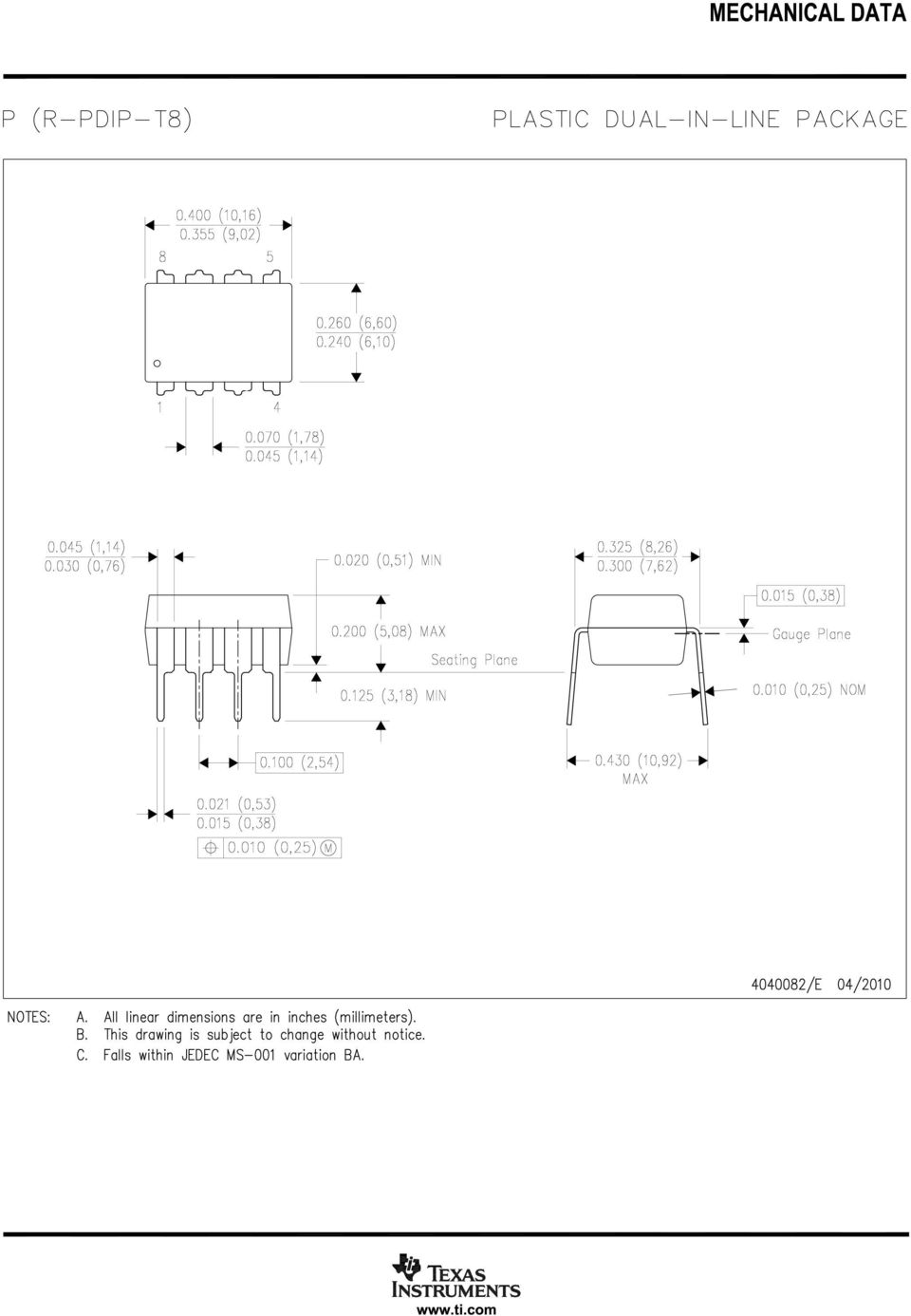
3 ABSOLUTE MAXIMUM RATINGS (1) +V CC... +6V Analog Input....3V to (+V CC +.3V) Logic Input....3V to (+V CC +.3V) Case Temperature C Junction Temperature C Storage Temperature C External Reference Voltage V NOTE: (1) Stresses above these ratings may permanently damage the device. PIN CONFIGURATION V REF +In In GND V CC DCLOCK CS/SHDN ELECTROSTATIC DISCHARGE SENSITIVITY Electrostatic discharge can cause damage ranging from performance degradation to complete device failure. Burr- Brown Corporation recommends that all integrated circuits be handled and stored using appropriate ESD protection methods. ESD damage can range from subtle performance degradation to complete device failure. Precision integrated circuits may be more susceptible to damage because very small parametric changes could cause the device not to meet published specifications. 8-Pin PDIP, 8-Lead SOIC, 8-Lead MSOP PIN ASSIGNMENTS PIN NAME DESCRIPTION 1 V REF Reference Input. 2 +In Non Inverting Input. 3 In Inverting Input. Connect to ground or to remote ground sense point. 4 GND Ground. 5 CS/SHDN Chip Select when LOW, Shutdown Mode when HIGH. 6 The serial output data word is comprised of 12 bits of data. In operation the data is valid on the falling edge of DCLOCK. The second clock pulse after the falling edge of CS enables the serial output. After one null bit the data is valid for the next 12 edges. 7 DCLOCK Data Clock synchronizes the serial data transfer and determines conversion speed. 8 +V CC Power Supply. PACKAGE/ORDERING INFORMATION MAXIMUM MAXIMUM INTEGRAL DIFFERENTIAL PACKAGE LINEARITY ERROR LINEARITY ERROR TEMPERATURE DRAWING PRODUCT (LSB) (LSB) RANGE PACKAGE NUMBER (1) P ±2 ±2 4 C to +85 C Plastic DIP 6 U ±2 ±2 4 C to +85 C SOIC 182 E ±2 ±2 4 C to +85 C MSOP 337 PB ±2 ±1 4 C to +85 C Plastic DIP 6 UB ±2 ±1 4 C to +85 C SOIC 182 EB ±2 ±1 4 C to +85 C MSOP 337 PC ±1 ±.75 4 C to +85 C Plastic DIP 6 UC ±1 ±.75 4 C to +85 C SOIC 182 EC ±1 ±.75 4 C to +85 C MSOP 337 NOTE: (1) For detailed drawing and dimension table, please see end of data sheet, or Appendix C of Burr-Brown IC Data Book. The information provided herein is believed to be reliable; however, BURR-BROWN assumes no responsibility for inaccuracies or omissions. BURR-BROWN assumes no responsibility for the use of this information, and all use of such information shall be entirely at the user s own risk. Prices and specifications are subject to change without notice. No patent rights or licenses to any of the circuits described herein are implied or granted to any third party. BURR-BROWN does not authorize or warrant any BURR-BROWN product for use in life support devices and/or systems. 3

4 TYPICAL PERFORMANCE CURVES At T A = +25 C, V CC = +5V, V REF = +5V, f SAMPLE = 2kHz, and f CLK = 16 f SAMPLE, unless otherwise specified. Change in Offset (LSB) CHANGE IN OFFSET vs REFERENCE VOLTAGE Reference Voltage (V) Delta from 25 C (LSB) CHANGE IN OFFSET vs TEMPERATURE Temperature ( C) 4 CHANGE IN GAIN vs REFERENCE VOLTAGE.15 CHANGE IN GAIN vs TEMPERATURE Change in Gain (LSB) Delta from 25 C (LSB) Reference Voltage (V) Temperature ( C) Effective Number of Bits (rms) EFFECTIVE NUMBER OF BITS vs REFERENCE VOLTAGE Reference Voltage (V) Peak-to-Peak Noise (LSB) PEAK-TO-PEAK NOISE vs REFERENCE VOLTAGE Reference Voltage (V) 4
 Effective Number of Bits (rms) 12 11.75 11.5 11.25 11 1.75 1.5 1.25 EFFECTIVE NUMBER OF BITS vs REFERENCE VOLTAGE 1.")
5 TYPICAL PERFORMANCE CURVES (CONT) At T A = +25 C, V CC = +5V, V REF = +5V, f SAMPLE = 2kHz, and f CLK = 16 f SAMPLE, unless otherwise specified. Power Supply Rejection (db) POWER SUPPLY REJECTION vs RIPPLE FREQUENCY Ripple Frequency (khz) Amplitude (db) FREQUENCY SPECTRUM (248 Point FFT; f IN = 9.9kHz,.5dB) Frequency (khz) Spurious Free Dynamic Range and Signal-to-Noise Ratio (db) SPURIOUS FREE DYNAMIC RANGE and SIGNAL-TO-NOISE RATIO vs FREQUENCY 1 9 Spurious Free Dynamic Range Signal-to-Noise Ratio Frequency (khz) Total Harmonic Distortion (db) TOTAL HARMONIC DISTORTION vs FREQUENCY Frequency (khz) Signal-to-(Noise + Distortion) (db) SIGNAL-TO-(NOISE + DISTORTION) vs FREQUENCY Frequency (khz) Signal-to-(Noise Ratio Plus Distortion) (db) SIGNAL-TO-(NOISE + DISTORTION) vs INPUT LEVEL Input Level (db) 5
 Total Harmonic Distortion (db) TOTAL HARMONIC DISTORTION vs FREQUENCY 1 2 3 4 5 6 7 8 9 1 1 1 1 Frequency (khz)")
6 TYPICAL PERFORMANCE CURVES (CONT) At T A = +25 C, V CC = +5V, V REF = +5V, f SAMPLE = 2kHz, and f CLK = 16 f SAMPLE, unless otherwise specified. 1. INTEGRAL LINEARITY ERROR vs CODE 1. DIFFERENTIAL LINEARITY ERROR vs CODE Integral Linearity Error (LSB) Differential Linearity Error (LSB) Code Code.1 CHANGE IN INTEGRAL LINEARITY AND DIFFERENTIAL LINEARITY vs REFERENCE VOLTAGE 1 INPUT LEAKAGE CURRENT vs TEMPERATURE Delta from +5V Reference (LSB) Change in Differential Linearity (LSB) Change in Integral Linearity (LSB) Leakage Current (na) Reference Voltage (V) Temperature ( C) 45 SUPPLY CURRENT vs TEMPERATURE 3 POWER DOWN SUPPLY CURRENT vs TEMPERATURE 4 f SAMPLE = 2kHz 2.5 Supply Current (µa) f SAMPLE = 12.5kHz Supply Current (µa) Temperature ( C) Temperature ( C) 6
.1 55 4 25 25 7 85 Temperature ( C) 45 SUPPLY CURRENT vs TEMPERATURE 3 POWER DOWN SUPPLY CURRENT vs TEMPERATURE 4 f SAMPLE = 2kHz 2.")
7 TYPICAL PERFORMANCE CURVES (CONT) At T A = +25 C, V CC = +5V, V REF = +5V, f SAMPLE = 2kHz, and f CLK = 16 f SAMPLE, unless otherwise specified. 4 REFERENCE CURRENT vs SAMPLE RATE (Code = 71h) 55 REFERENCE CURRENT vs TEMPERATURE (Code = 71h) Reference Current (µa) Sample Rate (khz) Reference Current (µa) Temperature ( C) Delta from f SAMPLE = 2kHz (LSB) CHANGE IN INTEGRAL LINEARITY and DIFFERENTIAL LINEARITY vs SAMPLE RATE Change in Integral Linearity (LSB) Change in Differential Linearity (LSB) Sample Rate (khz) 7
 Change in Differential Linearity (LSB).")
8 THEORY OF OPERATION The is a classic successive approximation register (SAR) analog-to-digital (A/D) converter. The architecture is based on capacitive redistribution which inherently includes a sample/hold function. The converter is fabricated on a.6µ CMOS process. The architecture and process allow the to acquire and convert an analog signal at up to 2, conversions per second while consuming very little power. The requires an external reference, an external clock, and a single +5V power source. The external reference can be any voltage between 1mV and V CC. The value of the reference voltage directly sets the range of the analog input. The reference input current depends on the conversion rate of the. The external clock can vary between 1kHz (625Hz throughput) and 3.2MHz (2kHz throughput). The duty cycle of the clock is essentially unimportant as long as the minimum high and low times are at least 15ns. The minimum clock frequency is set by the leakage on the capacitors internal to the. The analog input is provided to two input pins: +In and In. When a conversion is initiated, the differential input on these pins is sampled on the internal capacitor array. While a conversion is in progress, both inputs are disconnected from any internal function. The digital result of the conversion is clocked out by the DCLOCK input and is provided serially, most significant bit first, on the pin. The digital data that is provided on the pin is for the conversion currently in progress there is no pipeline delay. It is possible to continue to clock the after the conversion is complete and to obtain the serial data least significant bit first. See the Digital Interface section for more information. ANALOG INPUT The +In and In input pins allow for a differential input signal. Unlike some converters of this type, the In input is not resampled later in the conversion cycle. When the converter goes into the hold mode, the voltage difference between +In and In is captured on the internal capacitor array. The range of the In input is limited to ±2mV. Because of this, the differential input can be used to reject only small signals that are common to both inputs. Thus, the In input is best used to sense a remote signal ground that may move slightly with respect to the local ground potential. The input current on the analog inputs depends on a number of factors: sample rate, input voltage, source impedance, and power down mode. Essentially, the current into the charges the internal capacitor array during the sample period. After this capacitance has been fully charged, there is no further input current. The source of the analog input voltage must be able to charge the input capacitance (25pF) to a 12-bit settling level within 1.5 clock cycles. When the converter goes into the hold mode or while it is in the power down mode, the input impedance is greater than 1GΩ. Care must be taken regarding the absolute analog input voltage. To maintain the linearity of the converter, the In input should not exceed GND ±2mV. The +In input should always remain within the range of GND 2mV to V CC +2mV. Outside of these ranges, the converter s linearity may not meet specifications. REFERENCE INPUT The external reference sets the analog input range. The will operate with a reference in the range of 1mV to V CC. There are several important implications of this. As the reference voltage is reduced, the analog voltage weight of each digital output code is reduced. This is often referred to as the LSB (least significant bit) size and is equal to the reference voltage divided by 496. This means that any offset or gain error inherent in the A/D converter will appear to increase, in terms of LSB size, as the reference voltage is reduced. The typical performance curves of Change in Offset vs Reference Voltage and Change in Gain vs Reference Voltage provide more information. The noise inherent in the converter will also appear to increase with lower LSB size. With a 5V reference, the internal noise of the converter typically contributes only.16 LSB peak-to-peak of potential error to the output code. When the external reference is 1mV, the potential error contribution from the internal noise will be 5 times larger 8 LSBs. The errors due to the internal noise are gaussian in nature and can be reduced by averaging consecutive conversion results. For more information regarding noise, consult the typical performance curves Effective Number of Bits vs Reference Voltage and Peak-to-Peak Noise vs Reference Voltage. The effective number of bits (ENOB) figure is calculated based on the converter s signal-to-(noise + distortion) ratio with a 1kHz, db input signal. SINAD is related to ENOB as follows: SINAD = 6.2 ENOB With lower reference voltages, extra care should be taken to provide a clean layout including adequate bypassing, a clean power supply, a low-noise reference, and a low-noise input signal. Because the LSB size is lower, the converter will also be more sensitive to external sources of error such as nearby digital signals and electromagnetic interference. The current that must be provided by the external reference will depend on the conversion result. The current is lowest at full-scale (FFFh) and is typically 25µA at a 2kHz conversion rate (25 C). For the same conditions, the current will increase as the input approaches zero, reaching 5µA at an output result of h. The current does not increase linearly, but depends, to some degree, on the bit pattern of the digital output. 8

9 The reference current diminishes directly with both conversion rate and reference voltage. As the current from the reference is drawn on each bit decision, clocking the converter more quickly during a given conversion period will not reduce the overall current drain from the reference. The reference current changes only slightly with temperature. See the curves, Reference Current vs Sample Rate and Reference Current vs Temperature in the Typical Performance Curves section for more information. DIGITAL INTERFACE SERIAL INTERFACE The communicates with microprocessors and other digital systems via a synchronous 3-wire serial interface as shown in Figure 1 and Table I. The DCLOCK signal synchronizes the data transfer with each bit being transmitted on the falling edge of DCLOCK. Most receiving systems will capture the bitstream on the rising edge of DCLOCK. However, if the minimum hold time for is acceptable, the system can use the falling edge of DCLOCK to capture each bit. A falling CS signal initiates the conversion and data transfer. The first 1.5 to 2. clock periods of the conversion cycle are used to sample the input signal. After the second falling DCLOCK edge, is enabled and will output a LOW value for one clock period. For the next 12 DCLOCK periods, will output the conversion result, most significant bit first. After the least significant bit (B) has been output, subsequent clocks will repeat the output data but in a least significant bit first format. After the most significant bit (B11) has been repeated, will tri-state. Subsequent clocks will have no effect on the converter. A new conversion is initiated only when CS has been taken HIGH and returned LOW. SYMBOL DESCRIPTION MIN TYP MAX UNITS t SMPL Analog Input Sample TIme Clk Cycles t CONV Conversion Time 12 Clk Cycles t CYC Throughput Rate 2 khz t CSD CS Falling to ns DCLOCK LOW t SUCS CS Falling to 3 ns DCLOCK Rising t hdo DCLOCK Falling to 15 ns Current Not Valid t ddo DCLOCK Falling to Next ns Valid t dis CS Rising to Tri-State 25 5 ns t en DCLOCK Falling to 5 1 ns Enabled t f Fall Time 7 1 ns t r Rise Time 6 1 ns TABLE I. Timing Specifications 4 C to +85 C. t CYC CS/SHDN DCLOCK t SUCS POWER DOWN t CSD NULL HI-Z BIT B11 B1 B9 B8 B7 B6 B5 B4 B3 B2 B1 B (1) t (MSB) SMPL t CONV t DATA HI-Z NULL BIT B11 B1 B9 B8 Note: (1) After completing the data transfer, if further clocks are applied with CS LOW, the ADC will output LSB-First data then followed with zeroes indefinitely. CS/SHDN t CYC t SUCS POWER DOWN DCLOCK t CSD NULL HI-Z BIT B11 B1 B9 B8 B7 B6 B5 B4 B3 B2 B1 B B1 B2 B3 B4 t (MSB) SMPL t CONV B5 B6 B7 B8 B9 B1 B11 (2) t DATA HI-Z Note: (2) After completing the data transfer, if further clocks are applied with CS LOW, the ADC will output zeroes indefinitely. t DATA : During this time, the bias current and the comparator power down and the reference input becomes a high impedance node, leaving the CLK running to clock out LSB-First data or zeroes. FIGURE 1. Basic Timing Diagrams. 9

10 1.4V 3kΩ V OH Test Point V OL 1pF C LOAD t r t f Load Circuit for t ddo, t r, and t f Voltage Waveforms for Rise and Fall TImes t r, and t f DCLOCK V IL Test Point V CC t ddo 3kΩ t dis Waveform 2, t en V OH V OL 1pF C LOAD t dis Waveform 1 t hdo Voltage Waveforms for Delay Times, t ddo Load Circuit for t dis and t den CS/SHDN V IH CS/SHDN Waveform 1 (1) 9% DCLOCK 1 2 t dis Waveform 2 (2) 1% DOUT V OL B11 Voltage Waveforms for t dis t en NOTES: (1) Waveform 1 is for an output with internal conditions such that the output is HIGH unless disabled by the output control. (2) Waveform 2 is for an output with internal conditions such that the output is LOW unless disabled by the output control. Voltage Waveforms for t en FIGURE 2. Timing Diagrams and Test Circuits for the Parameters in Table I. DATA FORMAT The output data from the is in Straight Binary format as shown in Table II. This table represents the ideal output code for the given input voltage and does not include the effects of offset, gain error, or noise. DESCRIPTION ANALOG VALUE Full Scale Range V REF DIGITAL OUTPUT: Least Significant V REF /496 STRAIGHT BINARY Bit (LSB) Full Scale V REF 1 LSB BINARY CODE HEX CODE FFF Midscale V REF /2 1 8 Midscale 1 LSB V REF /2 1 LSB FF Zero V Table II. Ideal Input Voltages and Output Codes. POWER DISSIPATION The architecture of the converter, the semiconductor fabrication process, and a careful design allow the to convert at up to a 2kHz rate while requiring very little power. Still, for the absolute lowest power dissipation, there are several things to keep in mind. The power dissipation of the scales directly with conversion rate. The first step to achieving the lowest power dissipation is to find the lowest conversion rate that will satisfy the requirements of the system. In addition, the is in power down mode under two conditions: when the conversion is complete and whenever CS is HIGH (see Figure 1). Ideally, each conversion should occur as quickly as possible, preferably, at a 3.2MHz clock rate. This way, the converter spends the longest possible time in the power down mode. This is very important as the 1
 Waveform 2 is for an output with internal conditions such that the output is LOW unless disabled by the output control. Voltage Waveforms for t en FIGURE 2.")
11 converter not only uses power on each DCLOCK transition (as is typical for digital CMOS components) but also uses some current for the analog circuitry, such as the comparator. The analog section dissipates power continuously, until the power down mode is entered. Figure 3 shows the current consumption of the versus sample rate. For this graph, the converter is clocked at 3.2MHz regardless of the sample rate CS is HIGH for the remaining sample period. Figure 4 also shows current consumption versus sample rate. However, in this case, the DCLOCK period is 1/16th of the sample period CS is HIGH for one DCLOCK cycle out of every 16. There is an important distinction between the power down mode that is entered after a conversion is complete and the full power down mode which is enabled when CS is HIGH. While both power down the analog section, the digital section is powered down only when CS is HIGH. Thus, if CS is left LOW at the end of a conversion and the converter is continually clocked, the power consumption will not be as low as when CS is HIGH. See Figure 5 for more information. By lowering the reference voltage, the requires less current to completely charge its internal capacitors on both the analog input and the reference input. This reduction in power dissipation should be weighed carefully against the resulting increase in noise, offset, and gain error as outlined in the Reference section. The power dissipation of the is reduced roughly 1% when the reference voltage and input range are changed from 5V to 1mV. SHORT CYCLING Another way of saving power is to utilize the CS signal to short cycle the conversion. Because the places the latest data bit on the line as it is generated, the converter can easily be short cycled. This term means that the conversion can be terminated at any time. For example, if only 8-bits of the conversion result are needed, then the conversion can be terminated (by pulling CS HIGH) after the 8th bit has been clocked out. This technique can be used to lower the power dissipation (or to increase the conversion rate) in those applications where an analog signal is being monitored until some condition becomes true. For example, if the signal is outside a predetermined range, the full 12-bit conversion result may not be needed. If so, the conversion can be terminated after the first n-bits, where n might be as low as 3 or 4. This results in lower power dissipation in both the converter and the rest of the system, as they spend more time in the power down mode. LAYOUT For optimum performance, care should be taken with the physical layout of the circuitry. This is particularly true if the reference voltage is low and/or the conversion rate is high. At 2kHz conversion rate, the makes a bit decision every 312ns. That is, for each subsequent bit deci- Supply Current (µa) T A = 25 C V CC = V REF = +5V f CLK = 3.2MHz Sample Rate (khz) FIGURE 3. Maintaining f CLK at the Highest Possible Rate Allows Supply Current to Drop Directly with Sample Rate. Supply Current (µa) T A = 25 C V CC = V REF = +5V f CLK = 16 f SAMPLE Sample Rate (khz) FIGURE 4. Scaling f CLK Reduces Supply Current Only Slightly with Sample Rate. Supply Current (µa) T A = 25 C V CC = V REF = +5V f CLK = 16 f SAMPLE CS LOW (GND) CS = HIGH (V CC ) Sample Rate (khz) FIGURE 5. Shutdown Current is Considerably Lower with CS HIGH than when CS is LOW. 11

12 sion, the digital output must be updated with the results of the last bit decision, the capacitor array appropriately switched and charged, and the input to the comparator settled to a 12-bit level all within one clock cycle. The basic SAR architecture is sensitive to spikes on the power supply, reference, and ground connections that occur just prior to latching the comparator output. Thus, during any single conversion for an n-bit SAR converter, there are n windows in which large external transient voltages can easily affect the conversion result. Such spikes might originate from switching power supplies, digital logic, and high power devices, to name a few. This particular source of error can be very difficult to track down if the glitch is almost synchronous to the converter s DCLOCK signal as the phase difference between the two changes with time and temperature, causing sporadic misoperation. With this in mind, power to the should be clean and well bypassed. A.1µF ceramic bypass capacitor should be placed as close to the package as possible. In addition, a 1 to 1µF capacitor and a 1Ω series resistor may be used to lowpass filter a noisy supply. The reference should be similarly bypassed with a.1µf capacitor. Again, a series resistor and large capacitor can be used to lowpass filter the reference voltage. If the reference voltage originates from an op amp, be careful that the opamp can drive the bypass capacitor without oscillation (the series resistor can help in this case). Keep in mind that while the draws very little current from the reference on average, there are higher instantaneous current demands placed on the external reference circuitry. Also, keep in mind that the offers no inherent rejection of noise or voltage variation in regards to the reference input. This is of particular concern when the reference input is tied to the power supply. Any noise and ripple from the supply will appear directly in the digital results. While high frequency noise can be filtered out as described in the previous paragraph, voltage variation due to the line frequency (5Hz or 6Hz), can be difficult to remove. The GND pin on the should be placed on a clean ground point. In many cases, this will be the analog ground. Avoid connecting the GND pin too close to the grounding point for a microprocessor, microcontroller, or digital signal processor. If needed, run a ground trace directly from the converter to the power supply connection point. The ideal layout will include an analog ground plane for the converter and associated analog circuitry. The In input pin should be connected directly to ground. In those cases where the is a large distance from the signal source and/or the circuit environment contains large EMI or RFI sources, the In input should be connected to the ground nearest the signal source. This should be done with a signal trace that is adjacent to the +In input trace. If appropriate, coax cable or twisted-pair wire can be used. APPLICATION CIRCUITS Figures 6, 7, and 8 show some typical application circuits for the. Figure 6 uses an and a multiplexer to provide for a flexible data acquisition circuit. A resistor string provides for various voltages at the multiplexer input. The selected voltage is buffered and driven into V REF. As shown in Figure 6, the input range of the is programmable to 1mV, 2mV, 3mV, or 4mV. The 1mV range would be useful for sensors such as the thermocouple shown. Figure 7 is more complex variation of Figure 6 with increased flexibility. In this circuit, a digital signal processor designed for audio applications is put to use in running three s and a DAC56. The DAC56 provides a variable voltage for V REF enabling the input range of the s to be programmed from 1mV to 3V. +5V +5V +5V R 8 46kΩ D 1 TC 1 TC 2 Thermocouple TC 3 ISO Thermal Block R 1 15kΩ R 2 59kΩ R 4 1kΩ R 6 1MΩ R 3 5kΩ C 3.1µF V REF C 4 1µF R 5 C 5 5Ω.1µF U 1 C 2.1µF DCLOCK CS/SHDN R 7 1Ω OPA237 U 2 µp C 1 1µF MUX A A 1 U 3 R 9 1kΩ R 1 1kΩ R 11 1kΩ R 12 1kΩ.4V.3V.2V.1V 3-Wire Interface U 4 FIGURE 6. Thermocouple Application Using a MUX to Scale the Input Range of the. 12

13 DSP564 WST V REF CS SDO + 1µF.1µF +In SDO1 In DCLOCK SDO2 SCKT SCKR Serial Audio Interface V REF CS SDI + 1µF.1µF +In SDI1 In DCLOCK WSR SCK/SCL + 1µF.1µF V REF +In In CS DCLOCK MISO/SDA MOSI/HA HREQ Serial Host Interface 1Ω 1Ω 1Ω DAC56 SS/HA2 V OUT LE CLK DATA FIGURE 7. Flexible Data Acquisition System. +5V 5Ω to 1Ω + 1µF to 1µF.1µF V REF V CC + 1µF to 1µF +In In GND CS DCLOCK Microcontroller FIGURE 8. Basic Data Acquisition System. The s and the DSP564 can all be placed into a power down mode. Or, the DSP564 can run the s at a full 3.2MHz clock rate while on-board software enables the s as needed. With additional glue logic, the DSP564 could be used to run multiple DAC56s or provide CS controls for each of the three s. Figure 8 shows a basic data acquisition system. The input range is V to 5V, as the reference input is connected directly to the +5V supply. The 5Ω to 1Ω resistor and 1µF to 1µF capacitor filter the microcontroller noise on the supply, as well as any high-frequency noise from the supply itself. The exact values should be picked such that the filter provides adequate rejection of the noise. 13

14 PACKAGE OPTION ADDENDUM 12-Feb-216 PACKAGING INFORMATION Orderable Device Status (1) Package Type Package Drawing Pins Package Qty Eco Plan E/25 ACTIVE VSSOP DGK 8 25 Green (RoHS E/25G4 ACTIVE VSSOP DGK 8 25 Green (RoHS E/2K5 ACTIVE VSSOP DGK 8 25 Green (RoHS E/2K5G4 ACTIVE VSSOP DGK 8 25 Green (RoHS EB/25 ACTIVE VSSOP DGK 8 25 Green (RoHS EB/25G4 ACTIVE VSSOP DGK 8 25 Green (RoHS EB/2K5 ACTIVE VSSOP DGK 8 25 Green (RoHS EB/2K5G4 ACTIVE VSSOP DGK 8 25 Green (RoHS EC/25 ACTIVE VSSOP DGK 8 25 Green (RoHS EC/25G4 ACTIVE VSSOP DGK 8 25 Green (RoHS EC/2K5 ACTIVE VSSOP DGK 8 25 Green (RoHS P LIFEBUY PDIP P 8 5 Green (RoHS PB LIFEBUY PDIP P 8 5 Green (RoHS PBG4 LIFEBUY PDIP P 8 5 Green (RoHS PC LIFEBUY PDIP P 8 5 Green (RoHS PCG4 LIFEBUY PDIP P 8 5 Green (RoHS PG4 LIFEBUY PDIP P 8 5 Green (RoHS (2) Lead/Ball Finish (6) MSL Peak Temp (3) Op Temp ( C) CU NIPDAUAG Level-2-26C-1 YEAR -4 to 85 A16 CU NIPDAUAG Level-2-26C-1 YEAR -4 to 85 A16 CU NIPDAUAG Level-2-26C-1 YEAR -4 to 85 A16 CU NIPDAUAG Level-2-26C-1 YEAR -4 to 85 A16 CU NIPDAUAG Level-2-26C-1 YEAR -4 to 85 A16 CU NIPDAUAG Level-2-26C-1 YEAR -4 to 85 A16 CU NIPDAUAG Level-2-26C-1 YEAR -4 to 85 A16 CU NIPDAUAG Level-2-26C-1 YEAR -4 to 85 A16 CU NIPDAUAG Level-2-26C-1 YEAR -4 to 85 A16 CU NIPDAUAG Level-2-26C-1 YEAR -4 to 85 A16 CU NIPDAUAG Level-2-26C-1 YEAR -4 to 85 A16 CU NIPDAU N / A for Pkg Type -4 to 85 P CU NIPDAU N / A for Pkg Type -4 to 85 P B CU NIPDAU N / A for Pkg Type -4 to 85 P B CU NIPDAU N / A for Pkg Type -4 to 85 P C CU NIPDAU N / A for Pkg Type -4 to 85 P C CU NIPDAU N / A for Pkg Type -4 to 85 P Device Marking (4/5) Samples Addendum-Page 1

15 PACKAGE OPTION ADDENDUM 12-Feb-216 Orderable Device Status (1) Package Type Package Drawing Pins Package Qty Eco Plan U ACTIVE SOIC D 8 75 Green (RoHS U/2K5 ACTIVE SOIC D 8 25 Green (RoHS U/2K5G4 ACTIVE SOIC D 8 25 Green (RoHS UB ACTIVE SOIC D 8 75 Green (RoHS UB/2K5 ACTIVE SOIC D 8 25 Green (RoHS UB/2K5G4 ACTIVE SOIC D 8 25 Green (RoHS UBG4 ACTIVE SOIC D 8 75 Green (RoHS UC ACTIVE SOIC D 8 75 Green (RoHS UC/2K5 ACTIVE SOIC D 8 25 Green (RoHS UC/2K5G4 ACTIVE SOIC D 8 25 Green (RoHS UCG4 ACTIVE SOIC D 8 75 Green (RoHS UG4 ACTIVE SOIC D 8 75 Green (RoHS (2) Lead/Ball Finish (6) MSL Peak Temp (3) Op Temp ( C) CU NIPDAU Level-2-26C-1 YEAR -4 to 85 ADS 7816U CU NIPDAU Level-2-26C-1 YEAR -4 to 85 ADS 7816U CU NIPDAU Level-2-26C-1 YEAR -4 to 85 ADS 7816U CU NIPDAU Level-2-26C-1 YEAR -4 to 85 ADS 7816U B CU NIPDAU Level-2-26C-1 YEAR -4 to 85 ADS 7816U B CU NIPDAU Level-2-26C-1 YEAR -4 to 85 ADS 7816U B CU NIPDAU Level-2-26C-1 YEAR -4 to 85 ADS 7816U B CU NIPDAU Level-2-26C-1 YEAR -4 to 85 ADS 7816U C CU NIPDAU Level-2-26C-1 YEAR -4 to 85 ADS 7816U C CU NIPDAU Level-2-26C-1 YEAR -4 to 85 ADS 7816U C CU NIPDAU Level-2-26C-1 YEAR -4 to 85 ADS 7816U C CU NIPDAU Level-2-26C-1 YEAR -4 to 85 ADS 7816U Device Marking (4/5) Samples (1) The marketing status values are defined as follows: ACTIVE: Product device recommended for new designs. LIFEBUY: TI has announced that the device will be discontinued, and a lifetime-buy period is in effect. NRND: Not recommended for new designs. Device is in production to support existing customers, but TI does not recommend using this part in a new design. PREVIEW: Device has been announced but is not in production. Samples may or may not be available. Addendum-Page 2
 Lead/Ball Finish (6) MSL Peak Temp (3) Op Temp")
16 PACKAGE OPTION ADDENDUM 12-Feb-216 OBSOLETE: TI has discontinued the production of the device. (2) Eco Plan - The planned eco-friendly classification: Pb-Free (RoHS), Pb-Free (RoHS Exempt), or Green (RoHS - please check for the latest availability information and additional product content details. TBD: The Pb-Free/Green conversion plan has not been defined. Pb-Free (RoHS): TI's terms "Lead-Free" or "Pb-Free" mean semiconductor products that are compatible with the current RoHS requirements for all 6 substances, including the requirement that lead not exceed.1% by weight in homogeneous materials. Where designed to be soldered at high temperatures, TI Pb-Free products are suitable for use in specified lead-free processes. Pb-Free (RoHS Exempt): This component has a RoHS exemption for either 1) lead-based flip-chip solder bumps used between the die and package, or 2) lead-based die adhesive used between the die and leadframe. The component is otherwise considered Pb-Free (RoHS compatible) as defined above. Green (RoHS : TI defines "Green" to mean Pb-Free (RoHS compatible), and free of Bromine (Br) and Antimony (Sb) based flame retardants (Br or Sb do not exceed.1% by weight in homogeneous material) (3) MSL, Peak Temp. - The Moisture Sensitivity Level rating according to the JEDEC industry standard classifications, and peak solder temperature. (4) There may be additional marking, which relates to the logo, the lot trace code information, or the environmental category on the device. (5) Multiple Device Markings will be inside parentheses. Only one Device Marking contained in parentheses and separated by a "~" will appear on a device. If a line is indented then it is a continuation of the previous line and the two combined represent the entire Device Marking for that device. (6) Lead/Ball Finish - Orderable Devices may have multiple material finish options. Finish options are separated by a vertical ruled line. Lead/Ball Finish values may wrap to two lines if the finish value exceeds the maximum column width. Important Information and Disclaimer:The information provided on this page represents TI's knowledge and belief as of the date that it is provided. TI bases its knowledge and belief on information provided by third parties, and makes no representation or warranty as to the accuracy of such information. Efforts are underway to better integrate information from third parties. TI has taken and continues to take reasonable steps to provide representative and accurate information but may not have conducted destructive testing or chemical analysis on incoming materials and chemicals. TI and TI suppliers consider certain information to be proprietary, and thus CAS numbers and other limited information may not be available for release. In no event shall TI's liability arising out of such information exceed the total purchase price of the TI part(s) at issue in this document sold by TI to Customer on an annual basis. Addendum-Page 3
: TI's terms \"Lead-Free\" or \"Pb-Free\" mean semiconductor products that are compatible with the current RoHS requirements for all 6 substances, including the requirement that lead not")
17 PACKAGE MATERIALS INFORMATION 13-Feb-216 TAPE AND REEL INFORMATION *All dimensions are nominal Device Package Type Package Drawing Pins SPQ Reel Diameter (mm) Reel Width W1 (mm) A (mm) B (mm) K (mm) P1 (mm) W (mm) Pin1 Quadrant E/25 VSSOP DGK Q1 E/2K5 VSSOP DGK Q1 EB/25 VSSOP DGK Q1 EB/2K5 VSSOP DGK Q1 EC/25 VSSOP DGK Q1 EC/2K5 VSSOP DGK Q1 U/2K5 SOIC D Q1 UB/2K5 SOIC D Q1 UC/2K5 SOIC D Q1 Pack Materials-Page 1

18 PACKAGE MATERIALS INFORMATION 13-Feb-216 *All dimensions are nominal Device Package Type Package Drawing Pins SPQ Length (mm) Width (mm) Height (mm) E/25 VSSOP DGK E/2K5 VSSOP DGK EB/25 VSSOP DGK EB/2K5 VSSOP DGK EC/25 VSSOP DGK EC/2K5 VSSOP DGK U/2K5 SOIC D UB/2K5 SOIC D UC/2K5 SOIC D Pack Materials-Page 2

19
20
21
22
23
24 IMPORTANT NOTICE Texas Instruments Incorporated and its subsidiaries (TI) reserve the right to make corrections, enhancements, improvements and other changes to its semiconductor products and services per JESD46, latest issue, and to discontinue any product or service per JESD48, latest issue. Buyers should obtain the latest relevant information before placing orders and should verify that such information is current and complete. All semiconductor products (also referred to herein as components ) are sold subject to TI s terms and conditions of sale supplied at the time of order acknowledgment. TI warrants performance of its components to the specifications applicable at the time of sale, in accordance with the warranty in TI s terms and conditions of sale of semiconductor products. Testing and other quality control techniques are used to the extent TI deems necessary to support this warranty. Except where mandated by applicable law, testing of all parameters of each component is not necessarily performed. TI assumes no liability for applications assistance or the design of Buyers products. Buyers are responsible for their products and applications using TI components. To minimize the risks associated with Buyers products and applications, Buyers should provide adequate design and operating safeguards. TI does not warrant or represent that any license, either express or implied, is granted under any patent right, copyright, mask work right, or other intellectual property right relating to any combination, machine, or process in which TI components or services are used. Information published by TI regarding third-party products or services does not constitute a license to use such products or services or a warranty or endorsement thereof. Use of such information may require a license from a third party under the patents or other intellectual property of the third party, or a license from TI under the patents or other intellectual property of TI. Reproduction of significant portions of TI information in TI data books or data sheets is permissible only if reproduction is without alteration and is accompanied by all associated warranties, conditions, limitations, and notices. TI is not responsible or liable for such altered documentation. Information of third parties may be subject to additional restrictions. Resale of TI components or services with statements different from or beyond the parameters stated by TI for that component or service voids all express and any implied warranties for the associated TI component or service and is an unfair and deceptive business practice. TI is not responsible or liable for any such statements. Buyer acknowledges and agrees that it is solely responsible for compliance with all legal, regulatory and safety-related requirements concerning its products, and any use of TI components in its applications, notwithstanding any applications-related information or support that may be provided by TI. Buyer represents and agrees that it has all the necessary expertise to create and implement safeguards which anticipate dangerous consequences of failures, monitor failures and their consequences, lessen the likelihood of failures that might cause harm and take appropriate remedial actions. Buyer will fully indemnify TI and its representatives against any damages arising out of the use of any TI components in safety-critical applications. In some cases, TI components may be promoted specifically to facilitate safety-related applications. With such components, TI s goal is to help enable customers to design and create their own end-product solutions that meet applicable functional safety standards and requirements. Nonetheless, such components are subject to these terms. No TI components are authorized for use in FDA Class III (or similar life-critical medical equipment) unless authorized officers of the parties have executed a special agreement specifically governing such use. Only those TI components which TI has specifically designated as military grade or enhanced plastic are designed and intended for use in military/aerospace applications or environments. Buyer acknowledges and agrees that any military or aerospace use of TI components which have not been so designated is solely at the Buyer's risk, and that Buyer is solely responsible for compliance with all legal and regulatory requirements in connection with such use. TI has specifically designated certain components as meeting ISO/TS16949 requirements, mainly for automotive use. In any case of use of non-designated products, TI will not be responsible for any failure to meet ISO/TS Products Applications Audio Automotive and Transportation Amplifiers amplifier.ti.com Communications and Telecom Data Converters dataconverter.ti.com Computers and Peripherals DLP Products Consumer Electronics DSP dsp.ti.com Energy and Lighting Clocks and Timers Industrial Interface interface.ti.com Medical Logic logic.ti.com Security Power Mgmt power.ti.com Space, Avionics and Defense Microcontrollers microcontroller.ti.com Video and Imaging RFID OMAP Applications Processors TI E2E Community e2e.ti.com Wireless Connectivity Mailing Address: Texas Instruments, Post Office Box 65533, Dallas, Texas Copyright 216, Texas Instruments Incorporated
Data sheet acquired from Harris Semiconductor SCHS078C -- Revised October 2003
 Data sheet acquired from Harris Semiconductor SCHS078C -- Revised October 2003 The CD4521B types are supplied in 16-lead dual-in-line plastic packages (E suffix), 16-lead small-outline packages (M, M96,
SDLS940A MARCH 1974 REVISED MARCH 1988. Copyright 1988, Texas Instruments Incorporated
 SN5490A, SN5492A, SN5493A, SN54LS90, SN54LS92, SN54LS93 SN7490A, SN7492A, SN7493A, SN74LS90, SN74LS92, SN74LS93 DECADE, DIVIDE-BY-TWELVE AND BINARY COUNTERS SDLS940A MARCH 1974 REVISED MARCH 1988 PRODUCTION
with Ultra-Fast Transient Response and High Light-Load Efficiency
 1 Adaptor 6-24V Optional N-FET Driver Ultra-Fast DPM Simplified Application Diagram Iin Ultra-Low Quiescent Current Enhanced Safety Features OCP, OVP, FET Short Support CPU Turbo Mode To System bq24715
12-Bit, 4-Channel Parallel Output Sampling ANALOG-TO-DIGITAL CONVERTER
 For most current data sheet and other product information, visit www.burr-brown.com 12-Bit, 4-Channel Parallel Output Sampling ANALOG-TO-DIGITAL CONVERTER FEATURES SINGLE SUPPLY: 2.7V to 5V 4-CHANNEL INPUT
CD4071B Quad 2-Input OR Gate CD4072B Dual 4-Input OR Gate CD4075B Triple 3-Input OR Gate
 Data sheet acquired from Harris Semiconductor SCHS056D Revised August 2003 CD4071B Quad 2-Input OR Gate CD4072B Dual 4-Input OR Gate CD4075B Triple 3-Input OR Gate CD4071B, CD4072B, and CD4075B OR gates
Data sheet acquired from Harris Semiconductor SCHS049C Revised October 2003
 Data sheet acquired from Harris Semiconductor SCHS049C Revised October 2003 CD4060B consists of an oscillator section and 14 ripple-carry binary counter stages. The oscillator configuration allows design
AMC1100: Replacement of Input Main Sensing Transformer in Inverters with Isolated Amplifier
 Application Report SLAA552 August 2012 AMC1100: Replacement of Input Main Sensing Transformer in Inverters with Isolated Amplifier Ambreesh Tripathi and Harmeet Singh Analog/Digital Converters ABSTRACT
LM556 LM556 Dual Timer
 LM556 LM556 Dual Timer Literature Number: SNAS549 LM556 Dual Timer General Description The LM556 Dual timing circuit is a highly stable controller capable of producing accurate time delays or oscillation.
Data sheet acquired from Harris Semiconductor SCHS020C Revised October 2003
 Data sheet acquired from Harris Semiconductor SCHS020C Revised October 2003 The CD4009UB and CD4010B types are supplied in 16-lead hermetic dual-in-line ceramic packages (F3A suffix), 16-lead dual-in-line
LM5030 LM5030 Application: DC - DC Converter Utilizing the Push-Pull Topology
 LM5030 LM5030 Application: DC - DC Converter Utilizing the Push-Pull Topology Literature Number: SNVA553 LM5030 Application DC DC Converter Utilizing the Push-Pull Topology 1 Push-Pull Topology D1 L +
 PACKAGE OPTION ADDENDUM www.ti.com 12-Jan-2006 PACKAGING INFORMATION Orderable Device Status (1) Package Type Package Drawing Pins Package Qty Eco Plan (2) Lead/Ball Finish MSL Peak Temp (3) 76005012A
Data sheet acquired from Harris Semiconductor SCHS067B Revised July 2003
 Data sheet acquired from Harris Semiconductor SCHS067B Revised July 2003 The CD4502B types are supplied in 16-lead hermetic dual-in-line ceramic packages (F3A suffix), 16-lead dual-in-line plastic packages
Application Note AN107
 Murata Balun for CC253x and CC254x LFB182G45BG2D280 By Fredrik Kervel Keywords Balun LFB182G45BG2D280 CC253x CC254x CC257x CC85xx 1 Introduction Murata s LFB182G45BG2D280 integrated balun is specially
Data sheet acquired from Harris Semiconductor SCHS087D Revised October 2003
 Data sheet acquired from Harris Semiconductor SCHS087D Revised October 2003 The CD4555B and CD4556B types are supplied in 16-lead hermetic dual-in-line ceramic packages (F3A suffix), 16-lead dual-in-line
FEATURES APPLICATIONS
 FEATURES DIGITALLY-CONTROLLED ANALOG VOLUME CONTROL: Four Independent Audio Channels Serial Control Interface Zero Crossing Detection Mute Function WIDE GAIN AND ATTENUATION RANGE: +31.5dB to 95.5dB with
AUDIO DIFFERENTIAL LINE RECEIVER. 0dB (G = 1)
") INA4 INA4 INA4 INA4 INA4 INA4 AUDIO DIFFERENTIAL LINE RECEIVERS db (G = ) FEATURES SINGLE AND DUAL VERSIONS LOW DISTORTION:.% at f = khz HIGH SLEW RATE: 4V/µs FAST SETTLING TIME: µs to.% WIDE SUPPLY RANGE:
INA4 INA4 INA4 INA4 INA4 INA4 AUDIO DIFFERENTIAL LINE RECEIVERS db (G = ) FEATURES SINGLE AND DUAL VERSIONS LOW DISTORTION:.% at f = khz HIGH SLEW RATE: 4V/µs FAST SETTLING TIME: µs to.% WIDE SUPPLY RANGE:
RF37S114 Tag-it HF-I Type 5 NFC, ISO/IEC 15693 Transponder, 4 mm 4 mm
 1 1 Product Folder Sample & Buy Technical Documents Tools & Software Support & Community RF37S114 SCBS907 NOVEMBER 2015 RF37S114 Tag-it HF-I Type 5 NFC, ISO/IEC 15693 Transponder, 4 mm 4 mm 1 Device Overview
Wide Bandwidth, Fast Settling Difet OPERATIONAL AMPLIFIER
 Wide Bandwidth, Fast Settling Difet OPERATIONAL AMPLIFIER FEATURES HIGH GAIN-BANDWIDTH: 35MHz LOW INPUT NOISE: 1nV/ Hz HIGH SLEW RATE: V/µs FAST SETTLING: 24ns to.1% FET INPUT: I B = 5pA max HIGH OUTPUT
54LS174,54LS175,DM54LS174,DM54LS175, DM74LS174,DM74LS175
 54LS174,54LS175,DM54LS174,DM54LS175, DM74LS174,DM74LS175 54LS174 DM54LS174 DM74LS174 54LS175 DM54LS175 DM74LS175 Hex/Quad D Flip-Flops with Clear Literature Number: SNOS290A 54LS174 DM54LS174 DM74LS174
LM709 LM709 Operational Amplifier
 LM709 LM709 Operational Amplifier Literature Number: SNOS659A LM709 Operational Amplifier General Description The LM709 series is a monolithic operational amplifier intended for general-purpose applications
 PACKAGE OPTION ADDENDUM www.ti.com 12-Jan-2006 PACKAGING INFORMATION Orderable Device Status (1) Package Type Package Drawing Pins Package Qty Eco Plan (2) Lead/Ball Finish MSL Peak Temp (3) 5962-9557401QCA
16-Bit, 10µs Sampling, CMOS ANALOG-to-DIGITAL CONVERTER
 JANUARY 1996 REVISED OCTOBER 2006 16-Bit, 10µs Sampling, CMOS ANALOG-to-DIGITAL CONVERTER FEATURES 100kHz min SAMPLING RATE STANDARD ±10V INPUT RANGE 86dB min SINAD WITH 20kHz INPUT ±3.0 LSB max INL DNL:
PACKAGE OPTION ADDENDUM
 PACKAGE OPTION ADDENDUM www.ti.com 10-Jun-2014 PACKAGING INFORMATION Orderable Device Status (1) Package Type Package Drawing Pins Package Qty Eco Plan (2) Lead/Ball Finish (6) MSL Peak Temp (3) Op Temp
AN-1733 Load Transient Testing Simplified
 Application Report... ABSTRACT The load transient test may be the simplest diagnostic tool available to instantly analyze the loop stability of a system: the visual appearance of the output voltage as
1OE 3B NC 3B V GND ORDERING INFORMATION. QFN RGY Tape and reel SN74CBT3125RGYR CU125. SOIC D Tape and reel SN74CBT3125DR
 SN74CBT3125 QUADRUPLE FET BUS SWITCH SCDS021I MAY 1995 REVISED SEPTEMBER 2002 Standard 125-Type Pinout (D, DB, DGV, and PW Packages) 5-Ω Switch Connection Between Two Ports TTL-Compatible Input Levels
LM138,LM338. LM138/LM338 5-Amp Adjustable Regulators. Literature Number: SNVS771A
 LM138,LM338 LM138/LM338 5-Amp Adjustable Regulators Literature Number: SNVS771A LM138/LM338 5-Amp Adjustable Regulators General Description The LM138 series of adjustable 3-terminal positive voltage regulators
LM388 LM388 1.5W Audio Power Amplifier
 LM388 LM388 1.5W Audio Power Amplifier Literature Number: SNOSBT8A LM388 1 5W Audio Power Amplifier General Description The LM388 is an audio amplifier designed for use in medium power consumer applications
DS8907 DS8907 AM/FM Digital Phase-Locked Loop Frequency Synthesizer
 DS8907 DS8907 AM/FM Digital Phase-Locked Loop Frequency Synthesizer Literature Number: SNOSBR1A DS8907 AM FM Digital Phase-Locked Loop Frequency Synthesizer General Description The DS8907 is a PLL synthesizer
Providing Continuous Gate Drive Using a Charge Pump
 Application Report Philip Meyer and John Tucker... Power Management Products ABSTRACT Certain applications require that output voltage regulation be maintained when the input voltage is only slightly higher
description typical application
 Overvoltage Protection and Lockout for 12 V, 5 V, 3.3 V Undervoltage Protection and Lockout for 5 V and 3.3 V Fault Protection Output With Open-Drain Output Stage Open-Drain Power Good Output Signal for
16-Bit DIGITAL-TO-ANALOG CONVERTER With Serial Data Interface
 SBAS0A JULY 997 REVISED NOVEMBER 00 -Bit DIGITAL-TO-ANALOG CONVERTER With Serial Data Interface FEATURES: SERIAL DIGITAL INTERFACE VOLTAGE OUTPUT: ±0V, ±V, 0 to +0V ± LSB INTEGRAL LINEARITY -BIT MONOTONIC
Stereo Audio Volume Control
 PGA2320 Stereo Audio Volume Control FEATURES DIGITALLY-CONTROLLED ANALOG VOLUME CONTROL: Two Independent Audio Channels Serial Control Interface Zero Crossing Detection Mute Function WIDE GAIN AND ATTENUATION
SN54LVT574, SN74LVT574 3.3-V ABT OCTAL EDGE-TRIGGERED D-TYPE FLIP-FLOPS WITH 3-STATE OUTPUTS
 SN54LVT574, SN74LVT574 3.3-V ABT OCTAL EDGE-TRIGGERED D-TYPE FLIP-FLOPS WITH 3-STATE OUTPUTS SCBS139D MAY 1992 REVISED JULY 1995 State-of-the-Art Advanced BiCMOS Technology (ABT) Design for 3.3-V Operation
24-Bit, 40kHz ANALOG-TO-DIGITAL CONVERTER
 SEPTEMBER 2 REVISED JUNE 26 24-Bit, 4kHz ANALOG-TO-DIGITAL CONVERTER FEATURES 24 BITS NO MISSING CODES 19 BITS EFFECTIVE RESOLUTION UP TO 4kHz DATA RATE LOW NOISE: 2.5ppm DIFFERENTIAL INPUTS INL:.15% (max)
Analysis of Power Supply Topologies for IGBT Gate Drivers in Industrial
 Application Report SLAA672 July 2015 Analysis of Power Supply Topologies for IGBT Gate Drivers in Industrial Sanjay Pithadia, N. Navaneeth Kumar ABSTRACT This application report explains different parameters
Application Report. 1 Description of the Problem. Jeff Falin... PMP Portable Power Applications ABSTRACT
 Application Report SLVA255 September 2006 Minimizing Ringing at the Switch Node of a Boost Converter Jeff Falin... PMP Portable Power Applications ABSTRACT This application report explains how to use proper
Regulating Pulse Width Modulator
 Regulating Pulse Width Modulator UC1526 FEATURES 8 To 35V Operation 5V Reference Trimmed To ±1% 1Hz To 400kHz Oscillator Range Dual 100mA Source/Sink Outputs Digital Current Limiting Double Pulse Suppression
INSTRUMENTATION AMPLIFIER With Precision Voltage Reference
 INSTRUMENTATION AMPLIFIER With Precision Voltage Reference FEATURES LOW QUIESCENT CURRENT: 46µA PRECISION VOLTAGE REFERENCE: 1.24V, 2.V, V or 1V SLEEP MODE LOW OFFSET VOLTAGE: 2µV max LOW OFFSET DRIFT:
3V Video Amplifier with 6dB Gain and Filter in SC70
 OPA360 SB0S294E DECEMBER 2003 REVISED SEPTEMBER 2006 3V Video Amplifier with 6dB Gain and Filter in SC70 FEATURES EXCELLENT VIDEO PERFORMANCE INTERNAL GAIN: 6dB 2-POLE RECONSTRUCTION FILTER SAG CORRECTION
Wireless Subwoofer TI Design Tests
 Wireless Subwoofer TI Design Tests This system design was tested for THD+N vs. frequency at 5 watts and 30 watts and THD+N vs. power at 00. Both the direct analog input and the wireless systems were tested.
APPLICATION NOTE BUILDING A QAM MODULATOR USING A GC2011 DIGITAL FILTER CHIP
 SLWA022 APPLICATION NOTE BUILDING A QAM MODULATOR USING A GC2011 DIGITAL CHIP October 6, 1994 1.0 INTRODUCTION This report describes how one can use the GC2011 Digital Filter chip to build digital modulators
NTE2053 Integrated Circuit 8 Bit MPU Compatible A/D Converter
 NTE2053 Integrated Circuit 8 Bit MPU Compatible A/D Converter Description: The NTE2053 is a CMOS 8 bit successive approximation Analog to Digital converter in a 20 Lead DIP type package which uses a differential
LMS8117A LMS8117A 1A Low-Dropout Linear Regulator
 LMS8117A LMS8117A 1A Low-Dropout Linear Regulator Literature Number: SNOS487E LMS8117A 1A Low-Dropout Linear Regulator General Description The LMS8117A is a series of low dropout voltage regulators with
24-Bit, 20kHz, Low-Power ANALOG-TO-DIGITAL CONVERTER
 ADS1251 ADS1251 MARCH 21 REVISED JUNE 29 24-Bit, 2kHz, Low-Power ANALOG-TO-DIGITAL CONVERTER FEATURES 24 BITS NO MISSING CODES 19 BITS EFFECTIVE RESOLUTION UP TO 2kHz DATA RATE LOW NOISE: 1.5ppm DIFFERENTIAL
description/ordering information
 SLLS047L FEBRUARY 1989 REVISED MARCH 2004 Meets or Exceeds TIA/EIA-232-F and ITU Recommendation V.28 Operates From a Single 5-V Power Supply With 1.0-F Charge-Pump Capacitors Operates Up To 120 kbit/s
Application Report. 1 Introduction. 2 Resolution of an A-D Converter. 2.1 Signal-to-Noise Ratio (SNR) Harman Grewal... ABSTRACT
 Harman Grewal... ABSTRACT") Application Report SLAA323 JULY 2006 Oversampling the ADC12 for Higher Resolution Harman Grewal... ABSTRACT This application report describes the theory of oversampling to achieve resolutions greater than
Application Report SLAA323 JULY 2006 Oversampling the ADC12 for Higher Resolution Harman Grewal... ABSTRACT This application report describes the theory of oversampling to achieve resolutions greater than
AN-225 IC Temperature Sensor Provides Thermocouple Cold-Junction
 Application Report AN-225 IC Temperature Sensor Provides Thermocouple Cold-Junction... ABSTRACT Two circuits using the LM335 for thermocouple cold-junction compensation have been described. With a single
High-Voltage, Internally Powered ISOLATION AMPLIFIER
 ISO17 High-Voltage, Internally Powered ISOLATION AMPLIFIER FEATURES SIGNAL AND POWER IN ONE TRIPLE-WIDE PACKAGE 8Vpk TEST VOLTAGE 5Vrms CONTINUOUS AC BARRIER RATING WIDE INPUT SIGNAL RANGE: 1V to 1V WIDE
CD4051B-Q1, CD4052B-Q1, CD4053B-Q1 CMOS ANALOG MULTIPLEXERS/DEMULTIPLEXERS WITH LOGIC LEVEL CONVERSION
 Features Qualified for Automotive Applications Wide Range of Digital and Analog Signal Levels Digital: V to 0 V Analog: 0 V P-P Low ON Resistance, Ω (Typ) Over V P-P Signal Input Range for = V High OFF
Calculating Gain for Audio Amplifiers
 Application eport SLOA105A October 003 evised September 005 Calculating Gain for Audio Amplifiers Audio Power Amplifiers ABSTACT This application report explains the different types of audio power amplifier
TL081 TL081 Wide Bandwidth JFET Input Operational Amplifier
 TL081 TL081 Wide Bandwidth JFET Input Operational Amplifier Literature Number: SNOSBW6A TL081 Wide Bandwidth JFET Input Operational Amplifier General Description The TL081 is a low cost high speed JFET
Design Note DN304. Cebal CCxxxx Development Tools USB Driver Installation Guide By Åsmund B. Bø. Keywords. 1 Introduction
 Cebal CCxxxx Development Tools USB Driver Installation Guide By Åsmund B. Bø Keywords Cebal Driver Windows x86 Windows x64 SmartRF Studio SmartRF Packet Sniffer SmartRF Flash Programmer SmartRF05EB SmartRF04EB
TMP100 EP DIGITAL TEMPERATURE SENSOR WITH I 2 C INTERFACE
 Controlled Baseline One Assembly/Test Site, One Fabrication Site Enhanced Diminishing Manufacturing Sources (DMS) Support Enhanced Product-Change Notification Qualification Pedigree Digital Output: I 2
TLC548C, TLC548I, TLC549C, TLC549I 8-BIT ANALOG-TO-DIGITAL CONVERTERS WITH SERIAL CONTROL
 Microprocessor Peripheral or Standalone Operation 8-Bit Resolution A/D Converter Differential Reference Input Voltages Conversion Time...17 µs Max Total Access and Conversion Cycles Per Second TLC548...up
Ultrasonic Sensing Basics for Liquid Level Sensing, Flow Sensing, and Fluid
 Application Report SNAA0A March 015 Revised June 015 Ultrasonic Sensing Basics for Liquid Level Sensing, Flow Sensing, and Fluid AmyLe ABSTRACT The need for accurate and reliable sensors is growing in
12-Bit, 8-Channel Sampling ANALOG-TO-DIGITAL CONVERTER with I 2 C Interface
 ADS7828 ADS7828 NOVEMBER 2001 - REVISED MARCH 2005 12-Bit, 8-Channel Sampling ANALOG-TO-DIGITAL CONVERTER with I 2 C Interface FEATURES 8-CHANNEL MULTIPLEXER 50kHz SAMPLING RATE NO MISSING CODES 2.7V TO
description V CC A CLR BO CO LOAD C D B Q B Q A DOWN UP Q C Q D GND D OR N PACKAGE (TOP VIEW) SDFS031A D3693, JANUARY 1991 REVISED OCTOBER 1993
 SDFS031A D3693, JANUARY 1991 REVISED OCTOBER 1993") High-Speed f max of 100 MHz Typical Parallel Asynchronous Load for Modulo-N Count Lengths Look-Ahead Circuitry Enhances Speed of Cascaded Counters Fully Synchronous in Count Modes Package Optio Include
High-Speed f max of 100 MHz Typical Parallel Asynchronous Load for Modulo-N Count Lengths Look-Ahead Circuitry Enhances Speed of Cascaded Counters Fully Synchronous in Count Modes Package Optio Include
V OUT. I o+ & I o- (typical) 2.3A & 3.3A. Package Type
 2.3A & 3.3A. Package Type") July 25 th, 2012 Automotive Grade AUIRS4427S DUAL LOW SIDE DRIVER Features Gate drive supply range from 6 V to 20 V CMOS Schmitt-triggered inputs 3.3V and 5V logic compatible Two independent gate drivers
July 25 th, 2012 Automotive Grade AUIRS4427S DUAL LOW SIDE DRIVER Features Gate drive supply range from 6 V to 20 V CMOS Schmitt-triggered inputs 3.3V and 5V logic compatible Two independent gate drivers
Design Note DN041. Using CC253X or CC254X with Dipole PCB Antennas. Keywords. 1 Introduction. By Espen Wium CC2530 CC2531 CC2533 CC2540 CC2541
 Using CC253X or CC254X with Dipole PCB Antennas By Espen Wium Keywords Half wave dipole RF Antenna Efficiency Gain TRP (Total Radiated Power) CC2530 CC2531 CC2533 CC2540 CC2541 1 Introduction Many RFICs
LM1851 LM1851 Ground Fault Interrupter
 LM1851 LM1851 Ground Fault Interrupter Literature Number: SNIS158 LM1851 Ground Fault Interrupter General Description The LM1851 is designed to provide ground fault protection for AC power outlets in consumer
SN55115, SN75115 DUAL DIFFERENTIAL RECEIVERS
 SN55115, SN75115 DUAL DIFFERENTIAL RECEIVERS Choice of Open-Collector or Active Pullup (Totem-Pole) Outputs Single 5-V Supply Differential Line Operation Dual-Channel Operation TTL Compatible ± 15-V Common-Mode
TS555. Low-power single CMOS timer. Description. Features. The TS555 is a single CMOS timer with very low consumption:
 Low-power single CMOS timer Description Datasheet - production data The TS555 is a single CMOS timer with very low consumption: Features SO8 (plastic micropackage) Pin connections (top view) (I cc(typ)
DC/DC LED Lighting Developer s Kit Hardware
 Reference Guide The DC/DC LED lighting developer s kit provides a great way to learn and experiment by using a single MCU to accurately control a series of LED strings and efficiently control the power
Design Note DN004. Folded Dipole Antenna for CC25xx By Audun Andersen. Keywords. 1 Introduction CC2500 CC2550 CC2510 CC2511
 Folded Dipole Antenna for CC25xx By Audun Andersen Keywords CC2500 CC2550 CC2510 CC2511 Folded Dipole PCB Antenna 2.4 GHz 1 Introduction This document describes a folded dipole PCB antenna design that
AN-311 Theory and Applications of Logarithmic Amplifiers
 Application Report... ABSTRACT A number of instrumentation applications can benefit from the use of logarithmic or exponential signal processing techniques. The design and use of logarithmic/exponential
ORDERING INFORMATION. TOP-SIDE MARKING PDIP N Tube SN74LS07N SN74LS07N PACKAGE. SOIC D Tape and reel SN74LS07DR
 The SN54LS07 and SN74LS17 are obsolete and are no longer supplied. Convert TTL Voltage Levels to MOS Levels High Sink-Current Capability Input Clamping Diodes Simplify System Design Open-Collector Driver
Multi-Transformer LED TV Power User Guide. Anderson Hsiao
 Multi-Transformer LED TV Power User Guide Anderson Hsiao Operation Range Input Range: 90Vac~264Vac 47Hz~63Hz Dimming Range: Reverse Signal 0V ~ 5V 100Hz ~200Hz 1%~100% Output Range :STBY-5V 20mA~1A 5V
Features. Modulation Frequency (khz) VDD. PLL Clock Synthesizer with Spread Spectrum Circuitry GND
 VDD. PLL Clock Synthesizer with Spread Spectrum Circuitry GND") DATASHEET IDT5P50901/2/3/4 Description The IDT5P50901/2/3/4 is a family of 1.8V low power, spread spectrum clock generators capable of reducing EMI radiation from an input clock. Spread spectrum technique
DATASHEET IDT5P50901/2/3/4 Description The IDT5P50901/2/3/4 is a family of 1.8V low power, spread spectrum clock generators capable of reducing EMI radiation from an input clock. Spread spectrum technique
Texas Instruments. FB PS LLC Test Report HVPS SYSTEM AND APPLICATION TEAM REVA
 Texas Instruments FB PS LLC Test Report HVPS SYSTEM AND APPLICATION TEAM REVA 12/05/2014 1 General 1.1 PURPOSE Provide the detailed data for evaluating and verifying the FB-PS-LLC. The FB-PS-LLC is a Full
LTC1390 8-Channel Analog Multiplexer with Serial Interface U DESCRIPTIO
 FEATRES -Wire Serial Digital Interface Data Retransmission Allows Series Connection with Serial A/D Converters Single V to ±V Supply Operation Analog Inputs May Extend to Supply Rails Low Charge Injection
CD4049UB, CD4050B. CMOS Hex Buffer/Converters. Applications. [ /Title (CD40 49UB, CD405 0B) /Subject. Ordering Information
 /Subject. Ordering Information") CD4049UB, CD4050B Data sheet acquired from Harris Semiconductor SCHS046I August 1998 - Revised May 2004 [ /Title (CD40 49UB, CD405 0B) /Subject (CMO S Hex Buffer/ Converters) /Autho r () /Keywords (Harris
CD4049UB, CD4050B Data sheet acquired from Harris Semiconductor SCHS046I August 1998 - Revised May 2004 [ /Title (CD40 49UB, CD405 0B) /Subject (CMO S Hex Buffer/ Converters) /Autho r () /Keywords (Harris
AAT3520/2/4 MicroPower Microprocessor Reset Circuit
 General Description Features PowerManager The AAT3520 series of PowerManager products is part of AnalogicTech's Total Power Management IC (TPMIC ) product family. These microprocessor reset circuits are
DATA SHEET. TDA1543 Dual 16-bit DAC (economy version) (I 2 S input format) INTEGRATED CIRCUITS
 (I 2 S input format) INTEGRATED CIRCUITS") INTEGRATED CIRCUITS DATA SHEET File under Integrated Circuits, IC01 February 1991 FEATURES Low distortion 16-bit dynamic range 4 oversampling possible Single 5 V power supply No external components required
INTEGRATED CIRCUITS DATA SHEET File under Integrated Circuits, IC01 February 1991 FEATURES Low distortion 16-bit dynamic range 4 oversampling possible Single 5 V power supply No external components required
TLC556, TLC556Y DUAL LinCMOS TIMERS
 TLC556, TLC556Y DUAL LinCMOS TIMERS ery Low Power Consumption...2 mw Typ at DD = 5 Capable of Operation in Astable Mode CMOS Output Capable of Swinging Rail to Rail High Output-Current Capability Sink
ESD Protection Exceeds JESD 22 I off. 2000-V Human-Body Model (A114-A) 200-V Machine Model (A115-A)
 200-V Machine Model (A115-A)") www.ti.com FEATURES SN74CBTLV3245A LOW-VOLTAGE OCTAL FET BUS SWITCH SCDS034M JULY 1997 REVISED AUGUST 2005 Standard '245-Type Pinout Latch-Up Performance Exceeds 250 ma Per 5-Ω Switch Connection Between
www.ti.com FEATURES SN74CBTLV3245A LOW-VOLTAGE OCTAL FET BUS SWITCH SCDS034M JULY 1997 REVISED AUGUST 2005 Standard '245-Type Pinout Latch-Up Performance Exceeds 250 ma Per 5-Ω Switch Connection Between
Cold-Junction-Compensated K-Thermocoupleto-Digital Converter (0 C to +1024 C)
") 19-2235; Rev 1; 3/02 Cold-Junction-Compensated K-Thermocoupleto-Digital General Description The performs cold-junction compensation and digitizes the signal from a type-k thermocouple. The data is output
19-2235; Rev 1; 3/02 Cold-Junction-Compensated K-Thermocoupleto-Digital General Description The performs cold-junction compensation and digitizes the signal from a type-k thermocouple. The data is output
Importing a SPICE NetList Into TINA9-TI
 Application Report Importing a SPICE NetList into TINA9-TI John Miller... Analog elab ABSTRACT This application note describes the procedure for importing an unencrypted SPICE netlist into TINA9-TI (available
STLQ015. 150 ma, ultra low quiescent current linear voltage regulator. Description. Features. Application
 150 ma, ultra low quiescent current linear voltage regulator Description Datasheet - production data Features SOT23-5L Input voltage from 1.5 to 5.5 V Very low quiescent current: 1.0 µa (typ.) at no load
TPS76901, TPS76912, TPS76915, TPS76918, TPS76925 TPS76927, TPS76928, TPS76930, TPS76933, TPS76950 ULTRALOW-POWER 100-mA LOW-DROPOUT LINEAR REGULATORS
 -ma Low-Dropout Regulator TPS76901, TPS76912, TPS76915, TPS76918, TPS76925 TPS76927, TPS76928, TPS76930,, TPS76950 ULTRALOW-POWER -ma LOW-DROPOUT LINEAR REGULATORS Available in 1.2-V, 1.5-V, 1.8-V, 2.5-V,
AN-1963 IEEE 1588 Synchronization Over Standard Networks Using the
 Application Report AN-963 IEEE 588 Synchronization Over Standard Networks Using the... ABSTRACT This application report describes a method of synchronization that provides much more accurate synchronization
µa7800 SERIES POSITIVE-VOLTAGE REGULATORS
 SLS056J MAY 976 REISED MAY 2003 3-Terminal Regulators Output Current up to.5 A Internal Thermal-Overload Protection High Power-Dissipation Capability Internal Short-Circuit Current Limiting Output Transistor
MM58274C MM58274C Microprocessor Compatible Real Time Clock
 MM58274C MM58274C Microprocessor Compatible Real Time Clock Literature Number: SNOS618A MM58274C Microprocessor Compatible Real Time Clock General Description The MM58274C is fabricated using low threshold
SN54HC574, SN74HC574 OCTAL EDGE-TRIGGERED D-TYPE FLIP-FLOPS WITH 3-STATE OUTPUTS
 Wide Operating Voltage Range of 2 V to 6 V High-Current 3-State Noninverting Outputs Drive Bus Lines Directly or Up To 15 LSTTL Loads Low Power Consumption, 80-μA Max I CC Typical t pd = 22 ns ±6-mA Output
APPLICATION BULLETIN
 APPLICATION BULLETIN Mailing Address: PO Box 11400 Tucson, AZ 85734 Street Address: 6730 S. Tucson Blvd. Tucson, AZ 85706 Tel: (602 746-1111 Twx: 910-952-111 Telex: 066-6491 FAX (602 889-1510 Immediate
Precision, Unity-Gain Differential Amplifier AMP03
 a FEATURES High CMRR: db Typ Low Nonlinearity:.% Max Low Distortion:.% Typ Wide Bandwidth: MHz Typ Fast Slew Rate: 9.5 V/ s Typ Fast Settling (.%): s Typ Low Cost APPLICATIONS Summing Amplifiers Instrumentation
ELECTROSTATIC DISCHARGE SENSITIVITY
 INA INA SBOSD DECEMBER REVISED JANUARY micropower, Single-Supply, CMOS Instrumentation Amplifier FEATURES LOW QUIESCENT CURRENT: µa/channel Shut Down: < µa HIGH GAIN ACCURACY: G =,.%, ppm/ C GAIN SET WITH
AVAILABLE OPTIONS SMALL OUTLINE (D)
") SLOS65D MARCH 1991 REVISED APRIL 22 2.5-V Virtual Ground for 5-V/GND Analog Systems High Output-Current Capability Sink or Source... 2 ma Typ Micropower Operation... 17 µa Typ Excellent Regulation Characteristics
SLOS65D MARCH 1991 REVISED APRIL 22 2.5-V Virtual Ground for 5-V/GND Analog Systems High Output-Current Capability Sink or Source... 2 ma Typ Micropower Operation... 17 µa Typ Excellent Regulation Characteristics
AUDIO BALANCED LINE DRIVERS
 DRV DRV DRV DRV DRV AUDIO BALAED LINE DRIVERS FEATURES BALAED OUTPUT LOW DISTORTION:.% at f = khz WIDE OUTPUT SWING: Vrms into Ω HIGH CAPACITIVE LOAD DRIVE HIGH SLEW RATE: V/µs WIDE SUPPLY RANGE: ±.V to
Precision High-Speed Difet OPERATIONAL AMPLIFIERS
 Precision High-Speed Difet OPERATIONAL AMPLIFIERS FEATURES VERY LOW NOISE: 4.5nV/ Hz at khz FAST SETTLING TIME: 55ns to.% 45ns to.% LOW V OS : µv max LOW DRIFT:.8µV/ C max LOW I B : 5pA max : Unity-Gain
4-20mA Current-Loop Transmitter
 4-0mA Current-Loop Transmitter SBOS44C SEPTEMBER 005 REVISED MAY 01 FEATURES LOW QUIESCENT CURRENT: 10μA 5V REGULATOR FOR EXTERNAL CIRCUITS LOW SPAN ERROR: 0.05% LOW NONLINEARITY ERROR: 0.00% WIDE-LOOP
August 2001 PMP Low Power SLVU051
 User s Guide August 2001 PMP Low Power SLVU051 IMPORTANT NOTICE Texas Instruments and its subsidiaries (TI) reserve the right to make changes to their products or to discontinue any product or service
Low-Power, Single-Supply, CMOS INSTRUMENTATION AMPLIFIERS
 INA INA INA INA Low-Power, Single-Supply, CMOS INSTRUMENTATION AMPLIFIERS SBOSC DECEMBER REVISED APRIL FEATURES DESIGNED FOR LOW COST HIGH GAIN ACCURACY: G =,.%, ppm/ C GAIN SET WITH EXT. RESISTORS FOR
AN-1405 DP83848 Single 10/100 Mb/s Ethernet Transceiver Reduced Media Independent Interface (RMII ) Mode
 Mode") Application Report SNLA076A October 2005 Revised April 2013 AN-1405 DP83848 Single 10/100 Mb/s Ethernet Transceiver Reduced Media... ABSTRACT This application report summarizes how a designer can take
Application Report SNLA076A October 2005 Revised April 2013 AN-1405 DP83848 Single 10/100 Mb/s Ethernet Transceiver Reduced Media... ABSTRACT This application report summarizes how a designer can take
AN-1900 LM3150 Evaluation Boards
 User's Guide 1 Introduction The LM3150 evaluation boards are designed to provide the design engineer with a fully functional power converter based on Constant On-Time with Emulated Ripple mode control
24-Bit, 96kHz BiCMOS Sign-Magnitude DIGITAL-TO-ANALOG CONVERTER
 49% FPO 24-Bit, 96kHz BiCMOS Sign-Magnitude DIGITAL-TO-ANALOG CONVERTER TM FEATURES SAMPLING FREQUEY (f S ): 16kHz to 96kHz 8X OVERSAMPLING AT 96kHz INPUT AUDIO WORD: 20-, 24-Bit HIGH PERFORMAE: Dynamic
ICS379. Quad PLL with VCXO Quick Turn Clock. Description. Features. Block Diagram
 Quad PLL with VCXO Quick Turn Clock Description The ICS379 QTClock TM generates up to 9 high quality, high frequency clock outputs including a reference from a low frequency pullable crystal. It is designed
High Common-Mode Rejection. Differential Line Receiver SSM2141. Fax: 781/461-3113 FUNCTIONAL BLOCK DIAGRAM FEATURES. High Common-Mode Rejection
 a FEATURES High Common-Mode Rejection DC: 00 db typ 60 Hz: 00 db typ 20 khz: 70 db typ 40 khz: 62 db typ Low Distortion: 0.00% typ Fast Slew Rate: 9.5 V/ s typ Wide Bandwidth: 3 MHz typ Low Cost Complements
ICS650-44 SPREAD SPECTRUM CLOCK SYNTHESIZER. Description. Features. Block Diagram DATASHEET
 DATASHEET ICS650-44 Description The ICS650-44 is a spread spectrum clock synthesizer intended for video projector and digital TV applications. It generates three copies of an EMI optimized 50 MHz clock
SN54LV163A, SN74LV163A 4-BIT SYNCHRONOUS BINARY COUNTERS
 SN54LV163A, SN74LV163A 4-BIT SYNCHRONOUS BINARY COUNTERS 2-V to 5.5-V V CC Operation Max t pd of 9.5 ns at 5 V Typical V OLP (Output Ground Bounce)
AP331A XX G - 7. Lead Free G : Green. Packaging (Note 2)
") Features General Description Wide supply Voltage range: 2.0V to 36V Single or dual supplies: ±1.0V to ±18V Very low supply current drain (0.4mA) independent of supply voltage Low input biasing current:
Features General Description Wide supply Voltage range: 2.0V to 36V Single or dual supplies: ±1.0V to ±18V Very low supply current drain (0.4mA) independent of supply voltage Low input biasing current: