MRF175GU MRF175GV The RF MOSFET Line 200/150W, 500MHz, 28V
|
|
|
- Vernon George
- 8 years ago
- Views:
Transcription
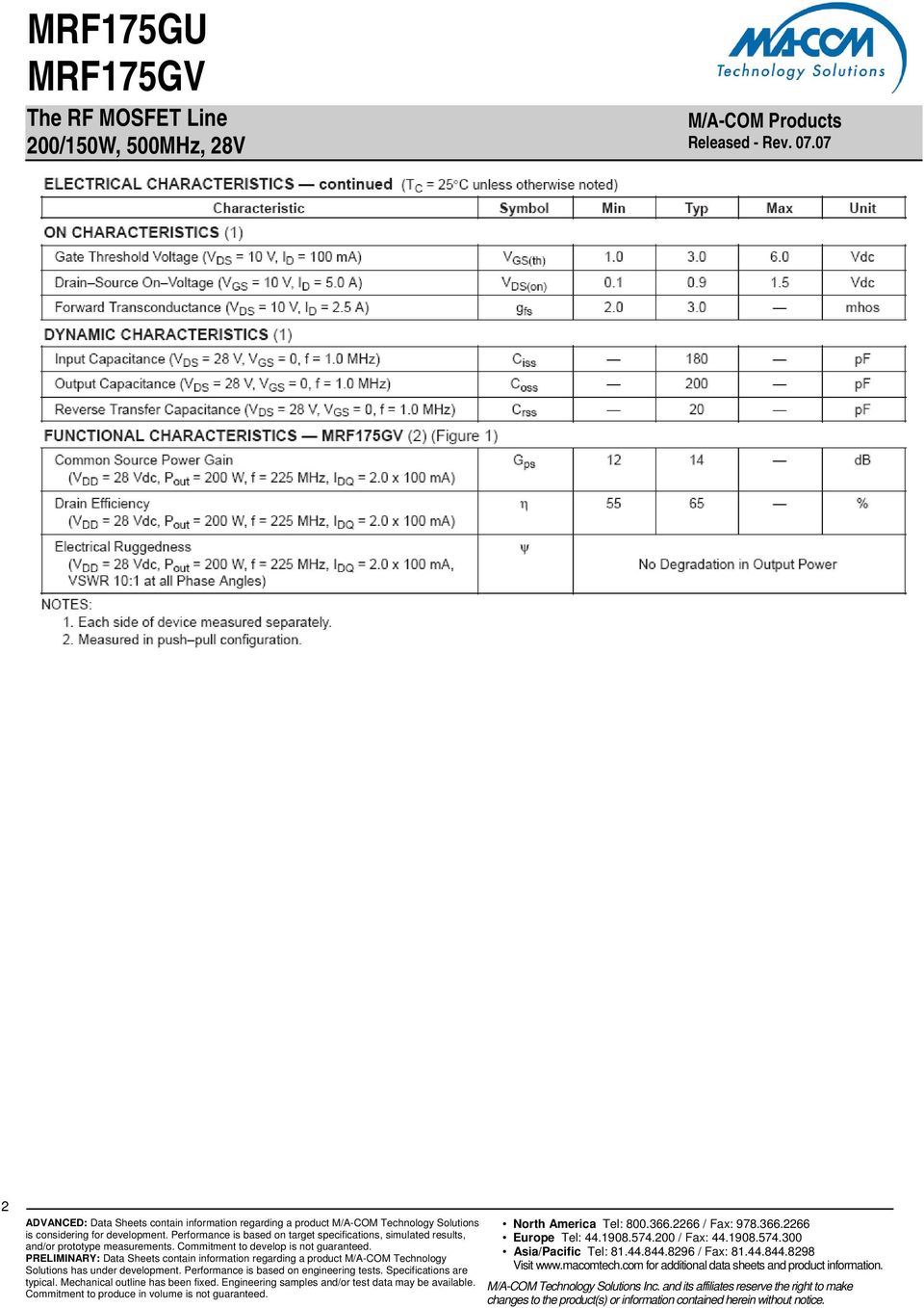
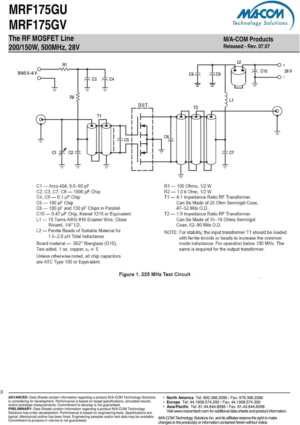
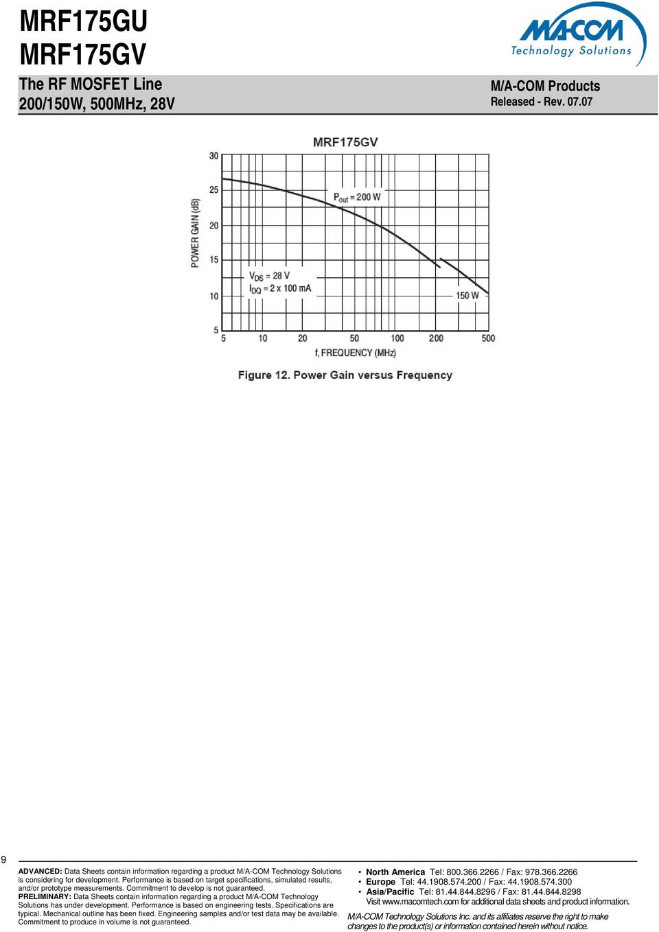
1 Designed for broadband commercial and military applications using push pull circuits at frequencies to 500 MHz. The high power, high gain and broadband performance of these devices makes possible solid state transmitters for FM broadcast or TV channel frequency bands. Product Image N Channel enhancement mode Guaranteed 28 V, 225 MHz ( V Suffix) Output power 200 W Power gain 14 db typ Efficiency 65% typ` 100% ruggedness tested at rated output power Low thermal resistance Low Crss 20 pf VDS = 28 V CASE , STYLE 2 1
 Output power 200 W Power gain 14 db typ")
2 2
3 3
4 4

5 5

6 6

7 7
8 8
9 9
10 10

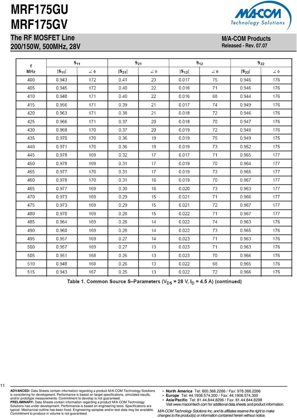
11 11
12 12

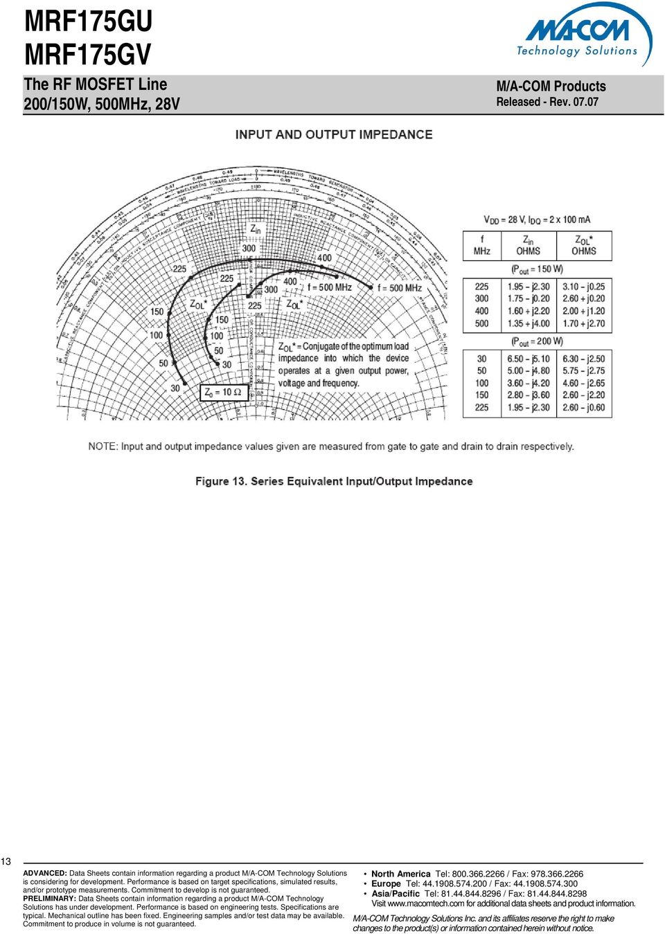
13 13
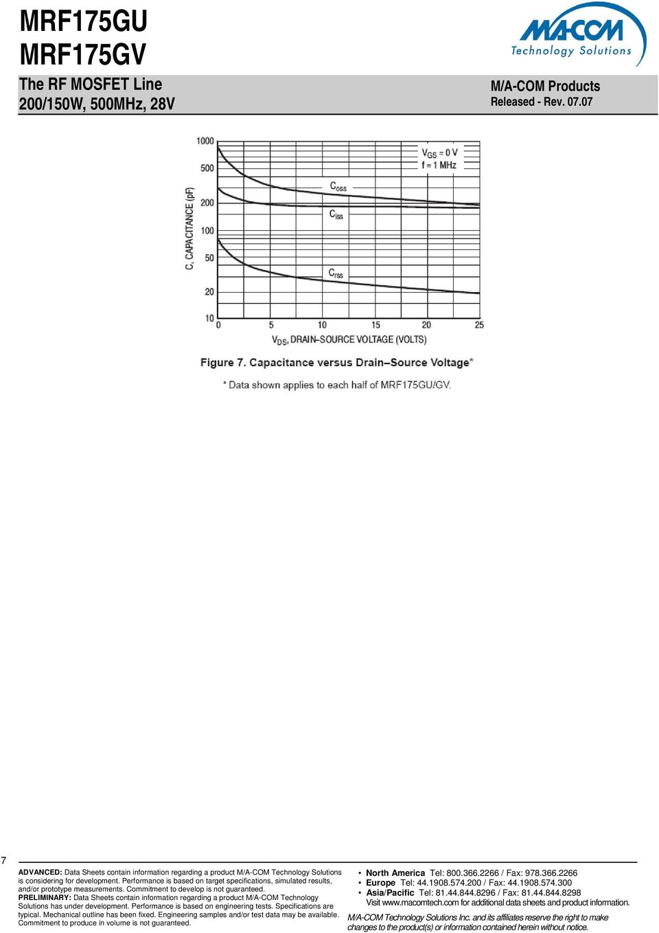
14 RF POWER MOSFET CONSIDERATIONS MOSFET CAPACITANCES The physical structure of a MOSFET results in capacitors between the terminals. The metal oxide gate structure determines the capacitors from gate to drain (Cgd), and gate to source (Cgs). The PN junction formed during the fabrication of the MOSFET results in a junction capacitance from drain to source (Cds). These capacitances are characterized as input (Ciss), output (Coss) and reverse transfer (Crss) capacitances on data sheets. The relationships between the inter terminal capacitances and those given on data sheets are shown below. The Ciss can be specified in two ways: 1. Drain shorted to source and positive voltage at the gate. 2. Positive voltage of the drain in respect to source and zerovolts at the gate. In the latter case the numbers are lower. However, neither method represents the actual operating conditions in RF applications. The Ciss givenin the electrical characteristics table was measured using method 2 above. It should be noted that Ciss, Coss, Crss are measured at zero drain current and are provided for general information about the device. They are not RF design parameters and no attempt should be made to use them as such. LINEARITY AND GAIN CHARACTERISTICS In addition to the typical IMD and power gain, data presented in Figure 3 may give the designer additional information on the capabilities of this device. The graph represents the small signal unity current gain frequency at a given drain current level. This is equivalent to ft for bipolar transistors. Since this test is performed at a fast sweep speed, heating of the device does not occur. Thus, in normal use, the highertemperatures may degrade these characteristics to some extent. DRAIN CHARACTERISTICS One figure of merit for a FET is its static resistance in the full on condition. This on resistance, VDS(on), occurs in the linear region of the output characteristic and is specified under specific test conditions for gate source voltage and drain current. For MOSFETs, VDS(on) has a positive temperature coefficient and constitutes an important design consideration at high temperatures, because it contributes to the power dissipation within the device. GATE CHARACTERISTICS The gate of the MOSFET is a polysilicon material, and is electrically isolated from the source by a layer of oxide. The input resistance is very high on the order of 109 ohms resulting in a leakage current of a few nanoamperes. Gate control is achieved by applying a positive voltage slightly in excess of the gate to source threshold voltage, VGS(th). Gate Voltage Rating Never exceed the gate voltage rating (or any of the maximum ratings on the front page). Exceeding the rated VGS can result in permanent damage to the oxide layer in the gate region. Gate Termination The gates of this device are essentially capacitors. Circuits that leave the gate open circuited or floating should be avoided. These conditions can result in turn on of the devices due to voltage build up on the input capacitor due to leakage currents or pickup. Gate Protection These devices do not have an internal monolithic zener diode from gate to source. If gate protection is required, an external zener diode is recommended. Using a resistor to keep the gate to source impedance low also helps damp transients and serves another important function. Voltage transients on the drain can be coupled to the gate through the parasitic gate drain capacitance. If the gate to source impedance and the rate of voltage change on the drain are both high, then the signal coupled to the gate may be large enough to exceed the gate threshold voltage and turn the device on. HANDLING CONSIDERATIONS When shipping, the devices should be transported only in antistatic bags or conductive foam. Upon removal from the packaging, careful handling procedures should be adhered to. Those handling the devices should wear grounding straps and devices not in the antistatic packaging should be kept in metal tote bins. MOSFETs should be handled by the case and not by the leads, and when testing the device, all leads should make good electrical contact before voltage is applied. As a final note, when placing the FET into the system it is designed for, soldering should be done with grounded equipment. DESIGN CONSIDERATIONS The MRF175G is a RF power N channel enhancement mode field effect transistor (FETs) designed for HF, VHF and 14
, output (Coss) and reverse transfer (Crss) capacitances on data sheets.")
15 RF POWER MOSFET CONSIDERATIONS MOSFET CAPACITANCES The physical structure of a MOSFET results in capacitors between the terminals. The metal oxide gate structure determines the capacitors from gate to drain (Cgd), and gate to source (Cgs). The PN junction formed during the fabrication of the MOSFET results in a junction capacitance from drain to source (Cds). These capacitances are characterized as input (Ciss), output (Coss) and reverse transfer (Crss) capacitances on data sheets. The relationships between the inter terminal capacitances and those given on data sheets are shown below. The Ciss can be specified in two ways: 1. Drain shorted to source and positive voltage at the gate. 2. Positive voltage of the drain in respect to source and zerovolts at the gate. In the latter case the numbers are lower. However, neither method represents the actual operating conditions in RF applications. The Ciss givenin the electrical characteristics table was measured using method 2 above. It should be noted that- Ciss, Coss, Crss are measured at zero drain current and are provided for general information about the device. They are not RF design parameters and no attempt should be made to use them as such. LINEARITY AND GAIN CHARACTERISTICS In addition to the typical IMD and power gain, data presented in Figure 3 may give the designer additional information on the capabilities of this device. The graph represents the small signal unity current gain frequency at a given drain current level. This is equivalent to ft for bipolar transistors. Since this test is performed at a fast sweep speed, heating of the device does not occur. Thus, in normal use, the higher temperatures may degrade these characteristics to some extent. DRAIN CHARACTERISTICS One figure of merit for a FET is its static resistance in the full on condition. This on resistance, VDS(on), occurs in the linear region of the output characteristic and is specified under specific test conditions for gate source voltage and drain current. For MOSFETs, VDS(on) has a positive temperature coefficient and constitutes an important design consideration at high temperatures, because it contributes to the power dissipation within the device. GATE CHARACTERISTICS The gate of the MOSFET is a polysilicon material, and is electrically isolated from the source by a layer of oxide. The input resistance is very high on the order of 109 ohms resulting in a leakage current of a few nanoamperes. Gate control is achieved by applying a positive voltage slightly in excess of the gate to source threshold voltage, VGS(th). Gate Voltage Rating Never exceed the gate voltage rating (or any of the maximum ratings on the front page). Exceeding the rated VGS can result in permanent damage to the oxide layer in the gate region. Gate Termination The gates of this device are essentially capacitors. Circuits that leave the gate open circuited or floating should be avoided. These conditions can result in turn on of the devices due to voltage build up on the input capacitor due to leakage currents or pickup. Gate Protection These devices do not have an internal monolithic zener diode from gate to source. If gate protection is required, an external zener diode is recommended. Using a resistor to keep the gate to source impedance low also helps damp transients and serves another important function. Voltage transients on the drain can be coupled to the gate through the parasitic gate drain capacitance. If the gate to source impedance and the rate of voltage change on the drain are both high, then the signal coupled to the gate may be large enough to exceed the gate threshold voltage and turn the device on. HANDLING CONSIDERATIONS When shipping, the devices should be transported only in antistatic bags or conductive foam. Upon removal from the packaging, careful handling procedures should be adhered to. Those handling the devices should wear grounding straps and devices not in the antistatic packaging should be kept in metal tote bins. MOSFETs should be handled by the case and not by the leads, and when testing the device, all leads should make good electrical contact before voltage is applied. As a final note, when placing the FET into the system it is designed for, soldering should be done with grounded equipment. DESIGN CONSIDERATIONS The MRF175G is a RF power N channel enhancement mode field effect transistor (FETs) designed for HF, VHF anduhf power amplifier applications. M/A-COM RF MOS- FETs feature a vertical structure with a planar design. M/A- 15
, output (Coss) and reverse transfer (Crss) capacitances on data sheets.")
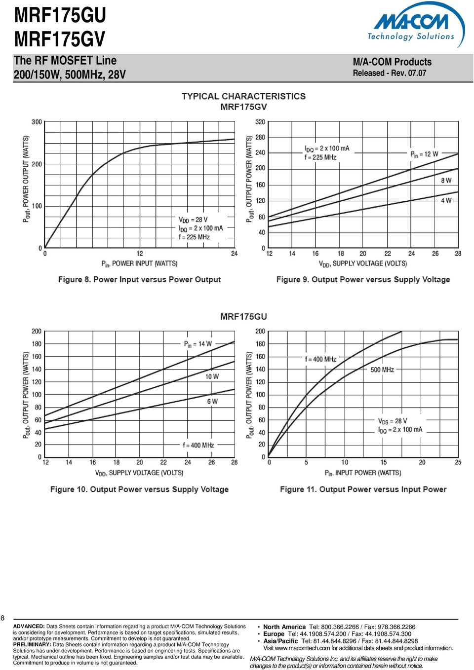
16 COM Application Note AN211A, FETs in Theory and Practice, is suggested reading for those not familiar with the construction and characteristics of FETs. The major advantages of RF power FETs include high gain, low noise, simple bias systems, relative immunity from thermal runaway, and the ability to withstand severely mismatched loads without suffering damage. Power output can be varied over a wide range with a low power dc control signal. DC BIAS The MRF175G is an enhancement mode FET and, therefore, does not conduct when drain voltage is applied. Drain current flows when a positive voltage is applied to the gate. RF power FETs require forward bias for optimum performance. The value of quiescent drain current (IDQ) is not critical for many applications. The MRF175G was characterized at IDQ = 100 ma, each side, which is the suggested minimumvalue of IDQ. For special applications such as linear amplification, IDQ may have to be selected to optimize the critical parameters. The gate is a dc open circuit and draws no current. Therefore, the gate bias circuit may be just a simple resistive divider network. Some applications may require a more elaborate bias sytem. GAIN CONTROL Power output of the MRF175G may be controlled from its rated value down to zero (negative gain) by varying the dc gate voltage. This feature facilitates the design of manual gain control, AGC/ALC and modulation systems. 16

DISCRETE SEMICONDUCTORS DATA SHEET. BLF244 VHF power MOS transistor
 DISCRETE SEMICONDUCTORS DATA SHEET September 1992 FEATURES High power gain Low noise figure Easy power control Good thermal stability Withstands full load mismatch Gold metallization ensures excellent
UGF09030. 30W, 1 GHz, 26V Broadband RF Power N-Channel Enhancement-Mode Lateral MOSFET
 30W, 1 GHz, 26V Broadband RF Power N-Channel Enhancement-Mode Lateral MOSFET Designed for base station applications in the frequency band 800MHz to 1000MHz. Rated with a minimum output power of 30W, it
MITSUBISHI RF MOSFET MODULE RA07H4047M
 MITSUBISHI RF MOSFET MODULE RA7H7M RoHS Compliance,-7MHz 7W.V, Stage Amp. For PORTABLE RADIO DESCRIPTION The RA7H7M is a 7-watt RF MOSFET Amplifier Module for.-volt portable radios that operate in the
RF Power LDMOS Transistors Enhancement--Mode Lateral MOSFETs
 Freescale Semiconductor Technical Data RF Power LDMOS Transistors Enhancement--Mode Lateral MOSFETs These 90 W RF power LDMOS transistors are designed for wideband RF power amplifiers covering the frequency
P D 215 1.25 Operating Junction Temperature T J 200 C Storage Temperature Range T stg 65 to +150 C
 SEMICONDUCTOR TECHNICAL DATA Order this document by /D The RF Line The is designed for output stages in band IV and V TV transmitter amplifiers. It incorporates high value emitter ballast resistors, gold
Features. Symbol JEDEC TO-220AB
 Data Sheet June 1999 File Number 2253.2 3A, 5V,.4 Ohm, N-Channel Power MOSFET This is an N-Channel enhancement mode silicon gate power field effect transistor designed for applications such as switching
BUZ11. 30A, 50V, 0.040 Ohm, N-Channel Power MOSFET. Features. [ /Title (BUZ1 1) /Subject. (30A, 50V, 0.040 Ohm, N- Channel. Ordering Information
 /Subject. (30A, 50V, 0.040 Ohm, N- Channel. Ordering Information") Data Sheet June 1999 File Number 2253.2 [ /Title (BUZ1 1) /Subject (3A, 5V,.4 Ohm, N- Channel Power MOS- FET) /Autho r () /Keywords (Intersil Corporation, N- Channel Power MOS- FET, TO- 22AB ) /Creator
Data Sheet June 1999 File Number 2253.2 [ /Title (BUZ1 1) /Subject (3A, 5V,.4 Ohm, N- Channel Power MOS- FET) /Autho r () /Keywords (Intersil Corporation, N- Channel Power MOS- FET, TO- 22AB ) /Creator
How To Make A Field Effect Transistor (Field Effect Transistor) From Silicon P Channel (Mos) To P Channel Power (Mos) (M2) (Mm2)
 From Silicon P Channel (Mos) To P Channel Power (Mos) (M2) (Mm2)") TPC811 TOSHIBA Field Effect Transistor Silicon P Channel MOS Type (U-MOS III) TPC811 Lithium Ion Battery Applications Notebook PC Applications Portable Equipment Applications Unit: mm Small footprint due
TPC811 TOSHIBA Field Effect Transistor Silicon P Channel MOS Type (U-MOS III) TPC811 Lithium Ion Battery Applications Notebook PC Applications Portable Equipment Applications Unit: mm Small footprint due
www.jameco.com 1-800-831-4242
 Distributed by: www.jameco.com 1-800-831-4242 The content and copyrights of the attached material are the property of its owner. LF411 Low Offset, Low Drift JFET Input Operational Amplifier General Description
SD4840/4841/4842/4843/4844
 CURRENT MODE PWM CONTROLLER WITH BUILT-IN HIGH VOLTAGE MOSFET DESCRIPTION SD4840/4841/4842/4843/4844 is a current mode PWM controller with low standby power and low start current for power switch. In standby
OptiMOS 3 Power-Transistor
 Type IPD36N4L G OptiMOS 3 Power-Transistor Features Fast switching MOSFET for SMPS Optimized technology for DC/DC converters Qualified according to JEDEC ) for target applications Product Summary V DS
CA723, CA723C. Voltage Regulators Adjustable from 2V to 37V at Output Currents Up to 150mA without External Pass Transistors. Features.
 CA73, CA73C Data Sheet April 1999 File Number 788. Voltage Regulators Adjustable from V to 37V at Output Currents Up to 1mA without External Pass Transistors The CA73 and CA73C are silicon monolithic integrated
NTE923 & NTE923D Integrated Circuit Precision Voltage Regulator
 NTE923 & NTE923D Integrated Circuit Precision Voltage Regulator Description: The NTE923 and NTE923D are voltage regulators designed primarily for series regulator applications. By themselves, these devices
N-channel enhancement mode TrenchMOS transistor
 FEATURES SYMBOL QUICK REFERENCE DATA Trench technology d V DSS = V Low on-state resistance Fast switching I D = A High thermal cycling performance Low thermal resistance R DS(ON) mω (V GS = V) g s R DS(ON)
IRF150 [REF:MIL-PRF-19500/543] 100V, N-CHANNEL. Absolute Maximum Ratings
![IRF150 [REF:MIL-PRF-19500/543] 100V, N-CHANNEL. Absolute Maximum Ratings](/thumbs/40/21333646.jpg "IRF150 [REF:MIL-PRF-19500/543] 100V, N-CHANNEL. Absolute Maximum Ratings") PD - 90337G REPETITIVE AVALANCHE AND dv/dt RATED HEXFET TRANSISTORS THRU-HOLE (TO-204AA/AE) Product Summary Part Number BVDSS RDS(on) ID IRF150 100V 0.055Ω 38A IRF150 JANTX2N6764 JANTXV2N6764 [REF:MIL-PRF-19500/543]
PD - 90337G REPETITIVE AVALANCHE AND dv/dt RATED HEXFET TRANSISTORS THRU-HOLE (TO-204AA/AE) Product Summary Part Number BVDSS RDS(on) ID IRF150 100V 0.055Ω 38A IRF150 JANTX2N6764 JANTXV2N6764 [REF:MIL-PRF-19500/543]
Design and Applications of HCPL-3020 and HCPL-0302 Gate Drive Optocouplers
 Design and Applications of HCPL-00 and HCPL-00 Gate Drive Optocouplers Application Note 00 Introduction The HCPL-00 (DIP-) and HCPL-00 (SO-) consist of GaAsP LED optically coupled to an integrated circuit
LM138 LM338 5-Amp Adjustable Regulators
 LM138 LM338 5-Amp Adjustable Regulators General Description The LM138 series of adjustable 3-terminal positive voltage regulators is capable of supplying in excess of 5A over a 1 2V to 32V output range
OptiMOS 3 Power-Transistor
 Type IPD6N3L G OptiMOS 3 Power-Transistor Features Fast switching MOSFET for SMPS Optimized technology for DC/DC converters Qualified according to JEDEC 1) for target applications Product Summary V DS
RF Power LDMOS Transistor High Ruggedness N--Channel Enhancement--Mode Lateral MOSFET
 Freescale Semiconductor Technical Data RF Power LDMOS Transistor High Ruggedness N--Channel Enhancement--Mode Lateral MOSFET RF power transistor suitable for both narrowband and broadband CW or pulse applications
LM134-LM234-LM334. Three terminal adjustable current sources. Features. Description
 Three terminal adjustable current sources Features Operates from 1V to 40V 0.02%/V current regulation Programmable from 1µA to 10mA ±3% initial accuracy Description The LM134/LM234/LM334 are 3-terminal
MADP-000504-10720T. Non Magnetic MELF PIN Diode
 MADP-54-172T Features High Power Handling Low Loss / Low Distortion Leadless Low Inductance MELF Package Non-Magnetic Surface Mountable RoHS Compliant MSL 1 Package Style 172 Dot Denotes Cathode Description
CMOS, the Ideal Logic Family
 CMOS, the Ideal Logic Family INTRODUCTION Let s talk about the characteristics of an ideal logic family. It should dissipate no power, have zero propagation delay, controlled rise and fall times, and have
Simple Broadband Solid-State Power Amplifiers
 Simple Broadband Solid-State Power Amplifiers Paul Wade W1GHZ 2014 w1ghz@arrl.net Recently, I was working on some VHF and UHF solid-state power amplifiers using LDMOS devices. These devices only take a
LM79XX Series 3-Terminal Negative Regulators
 LM79XX Series 3-Terminal Negative Regulators General Description The LM79XX series of 3-terminal regulators is available with fixed output voltages of b5v b8v b12v and b15v These devices need only one
SELF-OSCILLATING HALF-BRIDGE DRIVER
 Data Sheet No. PD60029 revj I2155&(PbF) (NOTE: For new designs, we recommend I s new products I2153 and I21531) SELF-OSCILLATING HALF-BIDGE DIE Features Floating channel designed for bootstrap operation
OBJECTIVE QUESTIONS IN ANALOG ELECTRONICS
 1. The early effect in a bipolar junction transistor is caused by (a) fast turn-on (c) large collector-base reverse bias (b)fast turn-off (d) large emitter-base forward bias 2. MOSFET can be used as a
CURRENT LIMITING SINGLE CHANNEL DRIVER V OFFSET. Packages
 Features Floating channel designed for bootstrap operation Fully operational to +5V Tolerant to negative transient voltage dv/dt immune Gate drive supply range from 12 to 18V Undervoltage lockout Current
OptiMOS Power-Transistor Product Summary
 OptiMOS Power-Transistor Product Summary V DS 55 V R DS(on),max 4) 35 mω Features Dual N-channel Logic Level - Enhancement mode AEC Q11 qualified I D 2 A PG-TDSON-8-4 MSL1 up to 26 C peak reflow 175 C
SIPMOS Small-Signal-Transistor
 SIPMOS Small-Signal-Transistor Features N-channel Depletion mode dv /dt rated Product Summary V DS V R DS(on),max 3.5 Ω I DSS,min.4 A Available with V GS(th) indicator on reel Pb-free lead plating; RoHS
EVALUATION KIT AVAILABLE Broadband, Two-Output, Low-Noise Amplifier for TV Tuner Applications MAX2130. Maxim Integrated Products 1
 9-86; Rev ; 8/ EVALUATION KIT AVAILABLE Broadband, Two-Output, Low-Noise General Description The broadband, low-distortion, low-noise, two-output amplifier performs preamp, loop-out, and buffer functions
1ED Compact A new high performance, cost efficient, high voltage gate driver IC family
 1ED Compact A new high performance, cost efficient, high voltage gate driver IC family Heiko Rettinger, Infineon Technologies AG, Am Campeon 1-12, 85579 Neubiberg, Germany, heiko.rettinger@infineon.com
Lecture 030 DSM CMOS Technology (3/24/10) Page 030-1
 Page 030-1") Lecture 030 DSM CMOS Technology (3/24/10) Page 030-1 LECTURE 030 - DEEP SUBMICRON (DSM) CMOS TECHNOLOGY LECTURE ORGANIZATION Outline Characteristics of a deep submicron CMOS technology Typical deep submicron
Lecture 030 DSM CMOS Technology (3/24/10) Page 030-1 LECTURE 030 - DEEP SUBMICRON (DSM) CMOS TECHNOLOGY LECTURE ORGANIZATION Outline Characteristics of a deep submicron CMOS technology Typical deep submicron
STP6N60FI N - CHANNEL ENHANCEMENT MODE POWER MOS TRANSISTOR
 N - CHANNEL ENHANCEMENT MODE POWER MOS TRANSISTOR TYPE VDSS RDS(on) ID STP6N60FI 600 V < 1.2 Ω 3.8 A TYPICAL R DS(on) =1Ω AVALANCHE RUGGED TECHNOLOGY 100% AVALANCHE TESTED REPETITIVE AVALANCHE DATA AT
Quad, Rail-to-Rail, Fault-Protected, SPST Analog Switches
 19-2418; Rev ; 4/2 Quad, Rail-to-Rail, Fault-Protected, General Description The are quad, single-pole/single-throw (SPST), fault-protected analog switches. They are pin compatible with the industry-standard
LM2576R. 3.0A, 52kHz, Step-Down Switching Regulator FEATURES. Applications DESCRIPTION TO-220 PKG TO-220V PKG TO-263 PKG ORDERING INFORMATION
 LM2576 FEATURES 3.3, 5.0, 12, 15, and Adjustable Output ersions Adjustable ersion Output oltage Range, 1.23 to 37 +/- 4% AG10Maximum Over Line and Load Conditions Guaranteed 3.0A Output Current Wide Input
TS321 Low Power Single Operational Amplifier
 SOT-25 Pin Definition: 1. Input + 2. Ground 3. Input - 4. Output 5. Vcc General Description The TS321 brings performance and economy to low power systems. With high unity gain frequency and a guaranteed
IRLR8729PbF IRLU8729PbF
 Applications l High Frequency Synchronous Buck Converters for Computer Processor Power l High Frequency Isolated DC-DC Converters with Synchronous Rectification for Telecom and Industrial Use Benefits
LF442 Dual Low Power JFET Input Operational Amplifier
 LF442 Dual Low Power JFET Input Operational Amplifier General Description The LF442 dual low power operational amplifiers provide many of the same AC characteristics as the industry standard LM1458 while
Description. 5k (10k) - + 5k (10k)
 - + 5k (10k)") THAT Corporation Low Noise, High Performance Microphone Preamplifier IC FEATURES Excellent noise performance through the entire gain range Exceptionally low THD+N over the full audio bandwidth Low power
THAT Corporation Low Noise, High Performance Microphone Preamplifier IC FEATURES Excellent noise performance through the entire gain range Exceptionally low THD+N over the full audio bandwidth Low power
Signal Types and Terminations
 Helping Customers Innovate, Improve & Grow Application Note Signal Types and Terminations Introduction., H, LV, Sinewave, Clipped Sinewave, TTL, PECL,,, CML Oscillators and frequency control devices come
S-Band Low Noise Amplifier Using the ATF-10136. Application Note G004
 S-Band Low Noise Amplifier Using the ATF-10136 Application Note G004 Introduction This application note documents the results of using the ATF-10136 in low noise amplifier applications at S band. The ATF-10136
Modifying the Yaesu FT-847 External 22.625 MHz Reference Input
 Modifying the Yaesu FT-847 External 22.625 MHz Reference Input David Smith VK3HZ Introduction This document describes the modification of an FT-847 to allow an external 22.625 MHz Reference oscillator
Lower Conduction Losses Low Thermal Resistance to PCB ( 0.5 C/W)
") PD -97428 IRFH5020PbF HEXFET Power MOSFET V DS 200 V 55 m: R DS(on) max (@V GS = V) Q g (typical) 36 nc R G (typical).9 : I D (@T c(bottom) = 25 C) 43 A PQFN 5X6 mm Applications Secondary Side Synchronous
PD -97428 IRFH5020PbF HEXFET Power MOSFET V DS 200 V 55 m: R DS(on) max (@V GS = V) Q g (typical) 36 nc R G (typical).9 : I D (@T c(bottom) = 25 C) 43 A PQFN 5X6 mm Applications Secondary Side Synchronous
DISCRETE SEMICONDUCTORS DATA SHEET. BFQ34 NPN 4 GHz wideband transistor. Product specification File under Discrete Semiconductors, SC14
 DISCRETE SEMICONDUCTORS DATA SHEET File under Discrete Semiconductors, SC4 September 995 DESCRIPTION PINNING NPN transistor encapsulated in a 4 lead SOTA envelope with a ceramic cap. All leads are isolated
The Pass Zen Amplifier: 10 Watts of Single-Stage Single-Ended Class A
 The Pass Zen Amplifier: 10 Watts of Single-Stage Single-Ended Class A I. "What is the sound of one transistor clapping?" There are two most essential principles to audio amplifier design. The first is
Advanced Monolithic Systems
 Advanced Monolithic Systems FEATURES Three Terminal Adjustable or Fixed oltages* 1.5, 1.8, 2.5, 2.85, 3.3 and 5. Output Current of 1A Operates Down to 1 Dropout Line Regulation:.2% Max. Load Regulation:.4%
Automotive MOSFETs in Linear Applications: Thermal Instability
 Application Note, V1.0, May 2005 Automotive MOSFETs in Linear Applications: Thermal Instability by Peter H. Wilson Automotive Power N e v e r s t o p t h i n k i n g. - 1 - Table of Content 1. Introduction...
CoolMOS TM Power Transistor
 CoolMOS TM Power Transistor Features New revolutionary high voltage technology Intrinsic fast-recovery body diode Extremely low reverse recovery charge Ultra low gate charge Extreme dv /dt rated Product
SSM3K335R SSM3K335R. 1. Applications. 2. Features. 3. Packaging and Pin Configuration. 2012-07-19 Rev.3.0. Silicon N-Channel MOS (U-MOS -H)
") MOSFETs Silicon N-Channel MOS (U-MOS-H) SSM3K335R SSM3K335R 1. Applications Power Management Switches DC-DC Converters 2. Features (1) 4.5-V gate drive voltage. (2) Low drain-source on-resistance : R DS(ON)
MOSFETs Silicon N-Channel MOS (U-MOS-H) SSM3K335R SSM3K335R 1. Applications Power Management Switches DC-DC Converters 2. Features (1) 4.5-V gate drive voltage. (2) Low drain-source on-resistance : R DS(ON)
TDA2040. 20W Hi-Fi AUDIO POWER AMPLIFIER
 20W Hi-Fi AUDIO POWER AMPLIFIER DESCRIPTION The TDA2040 is a monolithic integrated circuit in Pentawatt package, intended for use as an audio class AB amplifier. Typically it provides 22W output power
LM1084 5A Low Dropout Positive Regulators
 5A Low Dropout Positive Regulators General Description The LM1084 is a series of low dropout voltage positive regulators with a maximum dropout of 1.5 at 5A of load current. It has the same pin-out as
RF Power Field Effect Transistors N- Channel Enhancement- Mode Lateral MOSFETs
 Technical Data RF Power Field Effect Transistors N- Channel Enhancement- Mode Lateral MOSFETs Designed for GSM and GSM EDGE base station applications with frequencies from 864 to 894 MHz. Suitable for
OptiMOS TM Power-Transistor
 Type BSC28N6NS OptiMOS TM Power-Transistor Features Optimized for high performance SMPS, e.g. sync. rec. % avalanche tested Superior thermal resistance N-channel Qualified according to JEDEC ) for target
APT0001 By: Richard Frey, P.E. High Voltage, High Efficiency MOSFET RF Amplifiers Design Procedure and Examples
 APT0001 By: Richard Frey, P.E. High Voltage, High Efficiency MOSFET RF Amplifiers Design Procedure and Examples 1 High Voltage, High Efficiency MOSFET RF Amplifiers Design Procedure and Examples Introduction
KIA7805AF/API~KIA7824AF/API SEMICONDUCTOR TECHNICAL DATA THREE TERMINAL POSITIVE VOLTAGE REGULATORS 5V, 6V, 7V, 8V, 9V, 10V, 12V, 15V, 18V, 20V, 24V.
 SEMICONDUCTOR TECHNICAL DATA KIA785AF/API~KIA7824AF/API BIPOLAR LINEAR INTEGRATED THREE TERMINAL POSITIVE VOLTAGE REGULATORS 5V, 6V, 7V, 8V, 9V, 1V, 12V, 15V, 18V, 2V, 24V. FEATURES Internal Thermal Overload
Features Benefits Applications
 N9 N-Channel JFET Product Summary V GS(off) (V) V (BR)GSS Min (V) g fs Min SS Min (ma) 5 Features Benefits Applications Excellent High-Frequency Gain: Gps db @ MHz Very Low Noise: db @ MHz Very Low Distortion
AUTOMOTIVE MOSFET. C Soldering Temperature, for 10 seconds 300 (1.6mm from case )
") PD 9399A AUTOMOTIVE MOSFET Typical Applications Electric Power Steering (EPS) Antilock Braking System (ABS) Wiper Control Climate Control Power Door Benefits Advanced Process Technology Ultra Low OnResistance
PD 9399A AUTOMOTIVE MOSFET Typical Applications Electric Power Steering (EPS) Antilock Braking System (ABS) Wiper Control Climate Control Power Door Benefits Advanced Process Technology Ultra Low OnResistance
IRF830. N - CHANNEL 500V - 1.35Ω - 4.5A - TO-220 PowerMESH MOSFET
 IRF830 N - CHANNEL 500V - 1.35Ω - 4.5A - TO-220 PowerMESH MOSFET TYPE V DSS R DS(on) I D IRF830 500 V < 1.5 Ω 4.5 A TYPICAL R DS(on) = 1.35 Ω EXTREMELY HIGH dv/dt CAPABILITY 100% AVALANCHE TESTED VERY
MEETING TRANSIENT SPECIFICATIONS FOR ELECTRICAL SYSTEMS IN MILITARY VEHICLES
 MEETING TRANSIENT SPECIFICATIONS FOR ELECTRICAL SYSTEMS IN MILITARY VEHICLES By Arthur Jordan Sr. Applications Engineer, Vicor Electrical systems in military vehicles are normally required to meet stringent
Syllabus. For the trade of. Cable tv operator. Under Apprenticeship Training Scheme In the Informal Sector. Designed in 2002. Government of India
 Syllabus For the trade of Cable tv operator Under Apprenticeship Training Scheme In the Informal Sector Designed in 2002 Government of India Ministry of Labour (D.G.E.&T.) CENTRAL STAFF TRAINING AND RESEARCH
BLL6G1214L-250. 1. Product profile. LDMOS L-band radar power transistor. 1.1 General description. 1.2 Features and benefits. 1.
 BLL6G1214L-25 Rev. 1 16 February 212 Preliminary data sheet 1. Product profile 1.1 General description 25 W LDMOS power transistor intended for L-band radar applications in the 1.2 GHz to 1.4 GHz range.
LF412 Low Offset Low Drift Dual JFET Input Operational Amplifier
 LF412 Low Offset Low Drift Dual JFET Input Operational Amplifier General Description These devices are low cost high speed JFET input operational amplifiers with very low input offset voltage and guaranteed
C Soldering Temperature, for 10 seconds 300 (1.6mm from case )
") l Advanced Process Technology l Ultra Low On-Resistance l Dynamic dv/dt Rating l 75 C Operating Temperature l Fast Switching l Fully Avalanche Rated l Optimized for SMPS Applications Description Advanced
l Advanced Process Technology l Ultra Low On-Resistance l Dynamic dv/dt Rating l 75 C Operating Temperature l Fast Switching l Fully Avalanche Rated l Optimized for SMPS Applications Description Advanced
Application Note AN-940
 Application Note AN-940 How P-Channel MOSFETs Can Simplify Your Circuit Table of Contents Page 1. Basic Characteristics of P-Channel HEXFET Power MOSFETs...1 2. Grounded Loads...1 3. Totem Pole Switching
IRLR8743PbF IRLU8743PbF HEXFET Power MOSFET
 Applications l High Frequency Synchronous Buck Converters for Computer Processor Power l High Frequency Isolated DC-DC Converters with Synchronous Rectification for Telecom and Industrial Use l Lead-Free
W04 Transistors and Applications. Yrd. Doç. Dr. Aytaç Gören
 W04 Transistors and Applications W04 Transistors and Applications ELK 2018 - Contents W01 Basic Concepts in Electronics W02 AC to DC Conversion W03 Analysis of DC Circuits (self and condenser) W04 Transistors
DISCRETE SEMICONDUCTORS DATA SHEET M3D060. BLF177 HF/VHF power MOS transistor. Product specification Supersedes data of 1998 Jul 02.
 DISCRETE SEMICONDUCTORS DATA SHEET M3D6 Supersedes data of 1998 Jul 2 23 Jul 21 FEATURES High power gain Low intermodulation distortion Easy power control Good thermal stability Withstands full load mismatch.
LM117 LM317A LM317 3-Terminal Adjustable Regulator
 LM117 LM317A LM317 3-Terminal Adjustable Regulator General Description The LM117 series of adjustable 3-terminal positive voltage regulators is capable of supplying in excess of 1 5A over a 1 2V to 37V
Application Notes FREQUENCY LINEAR TUNING VARACTORS FREQUENCY LINEAR TUNING VARACTORS THE DEFINITION OF S (RELATIVE SENSITIVITY)
") FREQUENY LINEAR TUNING VARATORS FREQUENY LINEAR TUNING VARATORS For several decades variable capacitance diodes (varactors) have been used as tuning capacitors in high frequency circuits. Most of these
FREQUENY LINEAR TUNING VARATORS FREQUENY LINEAR TUNING VARATORS For several decades variable capacitance diodes (varactors) have been used as tuning capacitors in high frequency circuits. Most of these
BIASING OF CONSTANT CURRENT MMIC AMPLIFIERS (e.g., ERA SERIES) (AN-60-010)
 (AN-60-010)") BIASING OF CONSTANT CURRENT MMIC AMPLIFIERS (e.g., ERA SERIES) (AN-60-010) Introduction The Mini-Circuits family of microwave monolithic integrated circuit (MMIC) Darlington amplifiers offers the RF designer
BIASING OF CONSTANT CURRENT MMIC AMPLIFIERS (e.g., ERA SERIES) (AN-60-010) Introduction The Mini-Circuits family of microwave monolithic integrated circuit (MMIC) Darlington amplifiers offers the RF designer
Basic Electronics Prof. Dr. Chitralekha Mahanta Department of Electronics and Communication Engineering Indian Institute of Technology, Guwahati
 Basic Electronics Prof. Dr. Chitralekha Mahanta Department of Electronics and Communication Engineering Indian Institute of Technology, Guwahati Module: 2 Bipolar Junction Transistors Lecture-2 Transistor
TGF3015-SM. Applications. Product Features. Functional Block Diagram. General Description. Pin Configuration
 Applications Military radar Civilian radar Land mobile and military radio communications Test instrumentation Wideband or narrowband amplifiers Jammers Product Features Functional Block Diagram Frequency:
LM118/LM218/LM318 Operational Amplifiers
 LM118/LM218/LM318 Operational Amplifiers General Description The LM118 series are precision high speed operational amplifiers designed for applications requiring wide bandwidth and high slew rate. They
Diode Circuits. Operating in the Reverse Breakdown region. (Zener Diode)
") Diode Circuits Operating in the Reverse Breakdown region. (Zener Diode) In may applications, operation in the reverse breakdown region is highly desirable. The reverse breakdown voltage is relatively insensitive
Diode Circuits Operating in the Reverse Breakdown region. (Zener Diode) In may applications, operation in the reverse breakdown region is highly desirable. The reverse breakdown voltage is relatively insensitive
Low Noise, Matched Dual PNP Transistor MAT03
 a FEATURES Dual Matched PNP Transistor Low Offset Voltage: 100 V Max Low Noise: 1 nv/ Hz @ 1 khz Max High Gain: 100 Min High Gain Bandwidth: 190 MHz Typ Tight Gain Matching: 3% Max Excellent Logarithmic
Application Note AN-1068 reva
 Application Note AN-1068 reva Considerations for Designs Using Radiation-Hardened Solid State Relays By Alan Tasker Table of Contents Introduction Page Overview...1 The Contact...1 Actuation...1 The IR
Amplifier Teaching Aid
 Amplifier Teaching Aid Table of Contents Amplifier Teaching Aid...1 Preface...1 Introduction...1 Lesson 1 Semiconductor Review...2 Lesson Plan...2 Worksheet No. 1...7 Experiment No. 1...7 Lesson 2 Bipolar
GenTech Practice Questions
 GenTech Practice Questions Basic Electronics Test: This test will assess your knowledge of and ability to apply the principles of Basic Electronics. This test is comprised of 90 questions in the following
100V - 100W DMOS AUDIO AMPLIFIER WITH MUTE/ST-BY THERMAL SHUTDOWN STBY-GND
 TDA7294 100V - 100W DMOS AUDIO AMPLIFIER WITH MUTE/ST-BY VERY HIGH OPERATING VOLTAGE RANGE (±40V) DMOS POWER STAGE HIGH OUTPUT POWER (UP TO 100W MU- SIC POWER) MUTING/STAND-BY FUNCTIONS NO SWITCH ON/OFF
Chip Diode Application Note
 Chip Diode Application Note Introduction The markets of portable communications, computing and video equipment are challenging the semiconductor industry to develop increasingly smaller electronic components.
TL082 Wide Bandwidth Dual JFET Input Operational Amplifier
 TL082 Wide Bandwidth Dual JFET Input Operational Amplifier General Description These devices are low cost high speed dual JFET input operational amplifiers with an internally trimmed input offset voltage
COMMON-SOURCE JFET AMPLIFIER
 EXPERIMENT 04 Objectives: Theory: 1. To evaluate the common-source amplifier using the small signal equivalent model. 2. To learn what effects the voltage gain. A self-biased n-channel JFET with an AC
IRFP450. N - CHANNEL 500V - 0.33Ω - 14A - TO-247 PowerMESH MOSFET
 IRFP450 N - CHANNEL 500V - 0.33Ω - 14A - TO-247 PowerMESH MOSFET TYPE V DSS R DS(on) I D IRFP450 500 V < 0.4 Ω 14 A TYPICAL R DS(on) = 0.33 Ω EXTREMELY HIGH dv/dt CAPABILITY 100% AVALANCHE TESTED VERY
LM101A LM201A LM301A Operational Amplifiers
 LM101A LM201A LM301A Operational Amplifiers General Description The LM101A series are general purpose operational amplifiers which feature improved performance over industry standards like the LM709 Advanced
200V, N-CHANNEL. Absolute Maximum Ratings. Features: www.irf.com 1 PD - 90370
 PD - 90370 REPETITIVE AVALANCHE AND dv/dt RATED HEXFET TRANSISTORS THRU-HOLE (TO-204AA/AE) IRF240 200V, N-CHANNEL Product Summary Part Number BVDSS RDS(on) ID IRF240 200V 0.18Ω 18A The HEXFET technology
Application Note AN-1005
 Application Note AN-1005 Power MOSFET Avalanche Design Guidelines By Tim McDonald, Marco Soldano, Anthony Murray, Teodor Avram Table of Contents Page Table of Figures...3 Introduction...4 Overview...4
Bi-directional level shifter for I²C-bus and other systems.
 APPLICATION NOTE Bi-directional level shifter for I²C-bus and other Abstract With a single MOS-FET a bi-directional level shifter circuit can be realised to connect devices with different supply voltages
Oscillations and Regenerative Amplification using Negative Resistance Devices
 Oscillations and Regenerative Amplification using Negative Resistance Devices Ramon Vargas Patron rvargas@inictel.gob.pe INICTEL The usual procedure for the production of sustained oscillations in tuned
AAT4280 Slew Rate Controlled Load Switch
 General Description Features SmartSwitch The AAT4280 SmartSwitch is a P-channel MOSFET power switch designed for high-side load switching applications. The P-channel MOSFET device has a typical R DS(ON)
1.1 Silicon on Insulator a brief Introduction
 Table of Contents Preface Acknowledgements Chapter 1: Overview 1.1 Silicon on Insulator a brief Introduction 1.2 Circuits and SOI 1.3 Technology and SOI Chapter 2: SOI Materials 2.1 Silicon on Heteroepitaxial
NBB-402. RoHS Compliant & Pb-Free Product. Typical Applications
 Typical Applications Narrow and Broadband Commercial and Military Radio Designs Linear and Saturated Amplifiers 0 RoHS Compliant & Pb-Free Product NBB-402 CASCADABLE BROADBAND GaAs MMIC AMPLIFIER DC TO
Analog Devices Welcomes Hittite Microwave Corporation NO CONTENT ON THE ATTACHED DOCUMENT HAS CHANGED
 Analog Devices Welcomes Hittite Microwave Corporation NO CONTENT ON THE ATTACHED DOCUMENT HAS CHANGED www.analog.com www.hittite.com THIS PAGE INTENTIONALLY LEFT BLANK v2.71 HMC42ST8 / 42ST8E AMPLIFIER,.4-2.2
NOT RECOMMENDED FOR NEW DESIGN
 Technical Data RF Power Field Effect Transistor N-Channel Enhancement-Mode Lateral MOSFET Designed for broadband commercial and industrial applications with frequencies up to 00 MHz. The high gain and
LM386 Low Voltage Audio Power Amplifier
 Low Voltage Audio Power Amplifier General Description The LM386 is a power amplifier designed for use in low voltage consumer applications. The gain is internally set to 20 to keep external part count
DUAL%CHANNEL BROADBAND%LINEAR%AMPLIFIER Model&A800D
 ELECTRONICS AB DUAL%CHANNEL BROADBAND%LINEAR%AMPLIFIER Model&A800D & HIGH&VOLTAGE& FIXED&GAIN& BROADBAND & 800Vpp&60mA& 100x& DC&to&ca&200&kHz & LOW&OUTPUT&IMPEDANCE& HIGH&SLEW&RATE &
Data Sheet. HFBR-0600Z Series SERCOS Fiber Optic Transmitters and Receivers
 HFBR-0600Z Series SERCOS Fiber Optic Transmitters and Receivers Data Sheet SERCOS SERCOS is a SErial Realtime COmmunication System, a standard digital interface for communication between controls and drives
CAT4101TV. 1 A Constant-Current LED Driver with PWM Dimming
 A Constant-Current LED Driver with PWM Dimming Description The CAT4 is a constant current sink driving a string of high brightness LEDs up to A with very low dropout of.5 V at full load. It requires no
LM1036 Dual DC Operated Tone/Volume/Balance Circuit
 LM1036 Dual DC Operated Tone/Volume/Balance Circuit General Description The LM1036 is a DC controlled tone (bass/treble), volume and balance circuit for stereo applications in car radio, TV and audio systems.
S112-XHS. Description. Features. Agency Approvals. Applications. Absolute Maximum Ratings. Schematic Diagram. Ordering Information
 Description Features The S112-X is a bi-directional, single-pole, single-throw, normally open multipurpose solid-state relay. The circuit is composed of one input IR LED with a series limiting resistor
DC to 30GHz Broadband MMIC Low-Power Amplifier
 DC to 30GHz Broadband MMIC Low-Power Amplifier Features Integrated LFX technology: Simplified low-cost assembly Drain bias inductor not required Broadband 45GHz performance: Good gain (10 ± 1.25dB) 14.5dBm