Dependence of the thickness and composition of the HfO 2 /Si interface layer on annealing
|
|
|
- Douglas Bishop
- 9 years ago
- Views:
Transcription


1 Dependence of the thickness and composition of the HfO 2 /Si interface layer on annealing CINVESTAV-UNIDAD QUERETARO P.G. Mani-González and A. Herrera-Gomez gmani@qro.cinvestav.mx CINVESTAV 1
2 background Introduction ALD DC Sputtering XPS ARXPS Growth of HfO 2 films by ALD Caracterization by XPS Growth of TaN films by DC sputtering Caracterization by XPS Annealing of Si/HfO 2 /TaN Removed TaN Charaterization by XPS Conclusions CINVESTAV 2


3 Introduction High thermal stability and high dielectric constant. Get the composition and thickness of the HfO 2 /Si interface. CINVESTAV 3
 Si (100) RCA ALD M 1 M")

4 ALD (atomic layer deposition) Si/HfO 2 HfO 2 Si (001) Si (100) RCA ALD M 1 M 2 M 3 Pulse (seg) Drain (seg) H 2 O M 4 TDMA-Hf M 5 CINVESTAV 4
 P B = 6.4X10⁻⁶ torr CINVESTAV 5")
5 DC sputtering Si/HfO 2 /TaN TaN HfO 2 Ar N 2 Si (001) P B = 6.4X10⁻⁶ torr CINVESTAV 5
6 XPS X-ray source X ray Al K no-monochromatic M h = ev Mg K no-monochromatic h = ev electrons L K E K =h -E B CINVESTAV 6
7 Intensity Intensity Intensity Intensity XPS signal (a.u.) ARXPS concentric hemiespheric analyzer 3000 X-Ray Source 2500 Au 4f 7/ sample Au 4f 5/2 15 to 90 Au Si(001) Kinetic Energy Energy ev CINVESTAV 7
8 background Introduction ALD DC Sputtering XPS ARXPS Growth of HfO 2 films by ALD Caracterization by XPS Growth of TaN films by DC sputtering Caracterization by XPS Annealing of Si/HfO 2 /TaN Removed TaN Charaterization by XPS Conclusions CINVESTAV 8


9 Growth of HfO 2 in silicon wafer by ALD H 2 O (DI) TDMA-Hf (Tetrakis dimetilamino-hf) Growth condition P i = 2.039x10⁻¹ torr 275 C on the substrate 200 C on the wall 70 C on the cylinder TDMA-Hf CINVESTAV 9


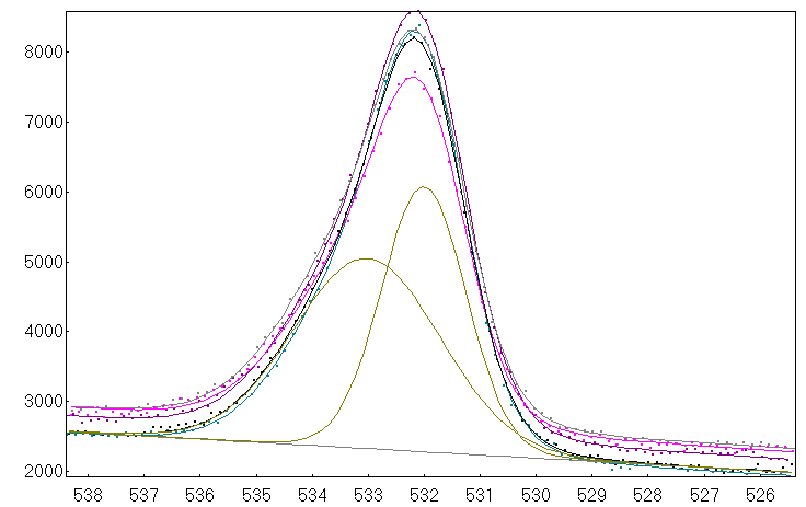
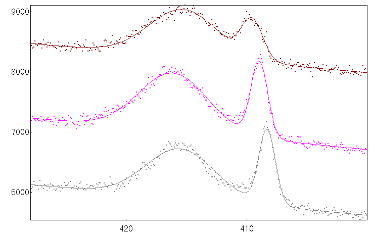
10 Intensity ARXPS in sample with 30 cycles Hf 4f C 1s Binding energy Si 2p O 1s CINVESTAV 10


11 Intensity Intensity Intensity Growth of HfO 2 /Si varying the number cycles Ciclos Si 2p Ciclos Hf 4f Binding energy Binding energy Ciclos O 1s Binding energy CINVESTAV 11
12 background Introduction ALD DC Sputtering XPS ARXPS Growth of HfO 2 films by ALD Caracterization by XPS Growth of TaN films by DC sputtering Caracterization by XPS Annealing of Si/HfO 2 /TaN Removed TaN Charaterization by XPS Conclusions CINVESTAV 12


13 TaN film grown by DC sputtering N 2 Ta P T = 2.6X10⁻⁴ torr t= 4 min P= 100 W Thickness= 1000 Å CINVESTAV 13


14 Intensity Characterization XPS in TaN films N 1s Binding energy Ta 4d N 10% Ta 4f N 5% N 2.5% CINVESTAV 14
 Ar flow (%) N (cm 3 ) Ar (cm 3 ) Thickness (Å) Resistivity (Ω cm) 2.5 97.5 0.6 24.4 1464 1.596E+02 5 95 1.3 23.7 1090 7.358E-02 10 90 2.5 22.")
15 Comparing TaN films grown by laser ablation and DC Sputtering Intensity Ta 4f Laser ablation * Binding energy N flow (%) Ar flow (%) N (cm 3 ) Ar (cm 3 ) Thickness (Å) Resistivity (Ω cm) E E E E-04 Laser A. * Dr. Wencel de la Cruz (CNyN) CINVESTAV 15


16 Intensity Intensity Intensity ARXPS in TaN films Ta associated in Ta 2 O 5 Ta 4f Ta associated in 0 TaN N 1s Binding Energy O 1s Binding Energy Binding Energy CINVESTAV 16
 (200) 2θ CINVESTAV")
17 Intensity Characterization XRD for TaN films (111) Laser ablation DC Sputtering (220) (200) 2θ CINVESTAV 17
18 background Introduction ALD DC Sputtering XPS ARXPS Growth of HfO 2 films by ALD Caracterization by XPS Growth of TaN films by DC sputtering Caracterization by XPS Annealing of Si/HfO 2 /TaN Removed TaN Charaterization by XPS Conclusions CINVESTAV 18

19 Thermal annealing and removed TaN for Si/HfO 2 /TaN N 2 Aire Aire N 2 T= C 10 seg T 2 Removed TaN NH 4 OH:H 2 O:H 2 O 2 10:1:1 to 85 C CINVESTAV 19


20 Intensity O associated in SiO 2 XPS after removed TaN film O 1s O associated in HfO 2 N 1s ev NO 2 * ev 1000 C 900 C 800 C 700 C ev ev Binding Energy Si 2p Ta 4f is not Hf 4f ev 99.4 ev ev ev * V.B. Wiertz, P. Bertrand, Identification of the n-containing functionalities introduced at the surface of ammonia plasma treated carbon fibres by combined TOF SIMS and XPS, Unité de Physico-Chimie et de Phys. Des Mat., Univ. Louvain 1348 Editor, Louvain. CINVESTAV 20


21 Thickness calculation Equations (model) and parameters employed in the calculations layers d 1 exp S above S S cos d I, exp i S r X r A S ss a, i cos 1 exp S i S cos S A 1 ~ (not exactly, but close) KE I I C Si, r, r C Si s s C Si 1 exp 1 Si asi sen 1 1 exp exp exp C C d SiO2 dc sen ac sen SiO2 sen exp d Hf HfO2 sen CINVESTAV 21
22 Parameters effective attenuation lengths cross section assymetry KE Si SiO2 HfO2 Carbon Si 2p Hf 4f N 1s O 1s C 1s Thickness The thicknesses were varied to reproduce the anions (Si, Hf and C) data C HfO 2 SiO nm 4.8 nm 2.1 nm Si (100) substrate CINVESTAV 22
23 Conclusions The annealing present a different phase of SiO2 and HfO2 moved the binding energy. increasing the cycles number, the signal of O assotiated to HfO2 increase. TaN is not present after of removed in the samples annealing With annealing the N is going to entrance to lattice of the HfO2 N 1s present a peak of correspond to NO2 is possible to introduce of HfON, SiON or both of them. The thickness was calculated with the equation CINVESTAV 23
24 Conclusiones Increase the SiO2 peak with annealing The suboxide in the Si 2p to continue increase with the temperature. We have a uniform and control in the grown of HfO2 films but is formed a SiO2 in the interface of HfO 2 /Si. is possible to see the contribution of TaO and TaN respect the angle resolution the Ta 2 O 5 is on the surface and N of the TaN is depth. CINVESTAV 24
Simultaneous data fitting in ARXPS
 NOTE Please find the following more updated document Resolving overlapping peaks in ARXPS data: The effect of noise and fitting method. J. Muñoz-Flores, A. Herrera-Gomez, J. Electron Spectrosc. Relat.
Etudes in situ et ex situ de multicouches C/FePt
 Etudes in situ et ex situ de multicouches C/FePt : influence de la température sur la structure et les propriétés s magnétiques D. Babonneau, G. Abadias, F. Pailloux Laboratoire de Physique des Matériaux
A Plasma Doping Process for 3D FinFET Source/ Drain Extensions
 A Plasma Doping Process for 3D FinFET Source/ Drain Extensions JTG 2014 Cuiyang Wang*, Shan Tang, Harold Persing, Bingxi Wood, Helen Maynard, Siamak Salimian, and Adam Brand Cuiyang_wang@amat.com Varian
Implementation Of High-k/Metal Gates In High-Volume Manufacturing
 White Paper Implementation Of High-k/Metal Gates In High-Volume Manufacturing INTRODUCTION There have been significant breakthroughs in IC technology in the past decade. The upper interconnect layers of
Optical Properties of Sputtered Tantalum Nitride Films Determined by Spectroscopic Ellipsometry
 Optical Properties of Sputtered Tantalum Nitride Films Determined by Spectroscopic Ellipsometry Thomas Waechtler a, Bernd Gruska b, Sven Zimmermann a, Stefan E. Schulz a, Thomas Gessner a a Chemnitz University
Coating Technology: Evaporation Vs Sputtering
 Satisloh Italy S.r.l. Coating Technology: Evaporation Vs Sputtering Gianni Monaco, PhD R&D project manager, Satisloh Italy 04.04.2016 V1 The aim of this document is to provide basic technical information
Al 2 O 3, Its Different Molecular Structures, Atomic Layer Deposition, and Dielectrics
 Al 2 O 3, Its Different Molecular Structures, Atomic Layer Deposition, and Dielectrics Mark Imus Douglas Sisk, Ph.D., Mentor Marian High School RET Program University of Notre Dame Project Proposal Tunneling
DIEGO TONINI MORPHOLOGY OF NIOBIUM FILMS SPUTTERED AT DIFFERENT TARGET SUBSTRATE ANGLE
 UNIVERSITÀ DEGLI STUDI DI PADOVA SCIENCE FACULTY MATERIAL SCIENCE DEGREE INFN LABORATORI NAZIONALI DI LEGNARO DIEGO TONINI MORPHOLOGY OF NIOBIUM FILMS SPUTTERED AT DIFFERENT TARGET SUBSTRATE ANGLE 2 QUESTIONS
Sputtered AlN Thin Films on Si and Electrodes for MEMS Resonators: Relationship Between Surface Quality Microstructure and Film Properties
 Sputtered AlN Thin Films on and Electrodes for MEMS Resonators: Relationship Between Surface Quality Microstructure and Film Properties S. Mishin, D. R. Marx and B. Sylvia, Advanced Modular Sputtering,
NANO SILICON DOTS EMBEDDED SIO 2 /SIO 2 MULTILAYERS FOR PV HIGH EFFICIENCY APPLICATION
 NANO SILICON DOTS EMBEDDED SIO 2 /SIO 2 MULTILAYERS FOR PV HIGH EFFICIENCY APPLICATION Olivier Palais, Damien Barakel, David Maestre, Fabrice Gourbilleau and Marcel Pasquinelli 1 Outline Photovoltaic today
Conductivity of silicon can be changed several orders of magnitude by introducing impurity atoms in silicon crystal lattice.
 CMOS Processing Technology Silicon: a semiconductor with resistance between that of conductor and an insulator. Conductivity of silicon can be changed several orders of magnitude by introducing impurity
X-ray photoelectron. Ba 0.5 Sr 0.5 Co 0.8 Fe 0.2 O 3 δ and La 0.6 Sr 0.4 Co 0.2 Fe 0.8 O 3 δ before and after thermal treatment and permeation test
 study on Ba 0.5 Sr 0.5 Co 0.8 Fe 0.2 O 3 δ and La 0.6 Sr 0.4 Co 0.2 Fe 0.8 O 3 δ before and after thermal treatment and permeation test Patrizia Rosa 1 1 Dipartimenti di Fisica Università degli Studi di
III. Wet and Dry Etching
 III. Wet and Dry Etching Method Environment and Equipment Advantage Disadvantage Directionality Wet Chemical Solutions Atmosphere, Bath 1) Low cost, easy to implement 2) High etching rate 3) Good selectivity
Spectroscopic Ellipsometry:
 Spectroscopic : What it is, what it will do, and what it won t do by Harland G. Tompkins Introduction Fundamentals Anatomy of an ellipsometric spectrum Analysis of an ellipsometric spectrum What you can
Supporting information
 Supporting information Ultrafast room-temperature NH 3 sensing with positively-gated reduced graphene oxide field-effect transistors Ganhua Lu 1, Kehan Yu 1, Leonidas E. Ocola 2, and Junhong Chen 1 * 1
2. Deposition process
 Properties of optical thin films produced by reactive low voltage ion plating (RLVIP) Antje Hallbauer Thin Film Technology Institute of Ion Physics & Applied Physics University of Innsbruck Investigations
Physical Properties and Functionalization of Low-Dimensional Materials
 Physical Properties and Functionalization of Low-Dimensional Materials Physics Department, University of Trieste Graduate School of Physics, XXVI cycle Supervisor: Co-supervisor: Prof. Alessandro BARALDI
Neuere Entwicklungen zur Herstellung optischer Schichten durch reaktive. Wolfgang Hentsch, Dr. Reinhard Fendler. FHR Anlagenbau GmbH
 Neuere Entwicklungen zur Herstellung optischer Schichten durch reaktive Sputtertechnologien Wolfgang Hentsch, Dr. Reinhard Fendler FHR Anlagenbau GmbH Germany Contents: 1. FHR Anlagenbau GmbH in Brief
Chapter 7-1. Definition of ALD
 Chapter 7-1 Atomic Layer Deposition (ALD) Definition of ALD Brief history of ALD ALD process and equipments ALD applications 1 Definition of ALD ALD is a method of applying thin films to various substrates
Introduction to VLSI Fabrication Technologies. Emanuele Baravelli
 Introduction to VLSI Fabrication Technologies Emanuele Baravelli 27/09/2005 Organization Materials Used in VLSI Fabrication VLSI Fabrication Technologies Overview of Fabrication Methods Device simulation
Vacuum Evaporation Recap
 Sputtering Vacuum Evaporation Recap Use high temperatures at high vacuum to evaporate (eject) atoms or molecules off a material surface. Use ballistic flow to transport them to a substrate and deposit.
Etching Etch Definitions Isotropic Etching: same in all direction Anisotropic Etching: direction sensitive Selectivity: etch rate difference between
 Etching Etch Definitions Isotropic Etching: same in all direction Anisotropic Etching: direction sensitive Selectivity: etch rate difference between 2 materials Other layers below one being etch Masking
BIOACTIVE COATINGS ON 316L STAINLESS STEEL IMPLANTS
 Trends Biomater. Artif. Organs. Vol. 17(2) pp 43-47 (2004) http//www.sbaoi.org BIOACTIVE COATINGS ON 316L STAINLESS STEEL IMPLANTS N. Ramesh Babu*,+, Sushant Manwatkar*, K. Prasada Rao* and T. S. Sampath
Exploring the deposition of oxides on silicon for photovoltaic cells by pulsed laser deposition
 Applied Surface Science 186 2002) 453±457 Exploring the deposition of oxides on silicon for photovoltaic cells by pulsed laser deposition Lianne M. Doeswijk a,*, Hugo H.C. de Moor b, Horst Rogalla a, Dave
Electrophoretic Gold Nanoparticles Depostion On Carbon Nanotubes For NO 2 Sensors
 European Network on New Sensing Technologies for Air Pollution Control and Environmental Sustainability - EuNetAir COST Action TD1105 2 nd International Workshop EuNetAir on New Sensing Technologies for
Advanced VLSI Design CMOS Processing Technology
 Isolation of transistors, i.e., their source and drains, from other transistors is needed to reduce electrical interactions between them. For technologies
h e l p s y o u C O N T R O L
 contamination analysis for compound semiconductors ANALYTICAL SERVICES B u r i e d d e f e c t s, E v a n s A n a l y t i c a l g r o u p h e l p s y o u C O N T R O L C O N T A M I N A T I O N Contamination
Results Overview Wafer Edge Film Removal using Laser
 Results Overview Wafer Edge Film Removal using Laser LEC- 300: Laser Edge Cleaning Process Apex Beam Top Beam Exhaust Flow Top Beam Scanning Top & Top Bevel Apex Beam Scanning Top Bevel, Apex, & Bo+om
Optical Hyperdoping: Transforming Semiconductor Band Structure for Solar Energy Harvesting
 Optical Hyperdoping: Transforming Semiconductor Band Structure for Solar Energy Harvesting 3G Solar Technologies Multidisciplinary Workshop MRS Spring Meeting San Francisco, CA, 5 April 2010 Michael P.
X-ray diffraction techniques for thin films
 X-ray diffraction techniques for thin films Rigaku Corporation Application Laboratory Takayuki Konya 1 Today s contents (PM) Introduction X-ray diffraction method Out-of-Plane In-Plane Pole figure Reciprocal
MOS (metal-oxidesemiconductor) 李 2003/12/19
 李 2003/12/19") MOS (metal-oxidesemiconductor) 李 2003/12/19 Outline Structure Ideal MOS The surface depletion region Ideal MOS curves The SiO 2 -Si MOS diode (real case) Structure A basic MOS consisting of three layers.
MOS (metal-oxidesemiconductor) 李 2003/12/19 Outline Structure Ideal MOS The surface depletion region Ideal MOS curves The SiO 2 -Si MOS diode (real case) Structure A basic MOS consisting of three layers.
Pulsed laser deposition of organic materials
 Pulsed laser deposition of organic materials PhD theses Gabriella Kecskeméti Department of Optics and Quantum Electronics University of Szeged Supervisor: Dr. Béla Hopp senior research fellow Department
Nanoelectronics 09. Atsufumi Hirohata Department of Electronics. Quick Review over the Last Lecture
 Nanoelectronics 09 Atsufumi Hirohata Department of Electronics 12:00 Wednesday, 4/February/2015 (P/L 006) Quick Review over the Last Lecture ( Field effect transistor (FET) ): ( Drain ) current increases
Lezioni di Tecnologie e Materiali per l Elettronica
 Lezioni di Tecnologie e Materiali per l Elettronica Danilo Manstretta danilo.manstretta@unipv.it microlab.unipv.it Outline Passive components Resistors Capacitors Inductors Printed circuits technologies
F ormation of Very Low Resistance Contact for Silicon Photovoltaic Cells. Baomin Xu, Scott Limb, Alexandra Rodkin, Eric Shrader, and Sean Gamer
 F ormation of Very Low Resistance Contact for Silicon Photovoltaic Cells Baomin Xu, Scott Limb, Alexandra Rodkin, Eric Shrader, and Sean Gamer Palo Alto Research Center, 3333 Coyote Hill Road, Palo Alto,
Glancing XRD and XRF for the Study of Texture Development in SmCo Based Films Sputtered Onto Silicon Substrates
 161 162 Glancing XRD and XRF for the Study of Texture Development in SmCo Based Films Sputtered Onto Silicon Substrates F. J. Cadieu*, I. Vander, Y. Rong, and R. W. Zuneska Physics Department Queens College
The study of deep-level emission center in ZnO films grown on c-al 2 O 3 substrates
 The study of deep-level emission center in ZnO films grown on c-al 2 O 3 substrates Guotong Du Yuantao Zhang, Jinzhong Wang, Yongguo Cui (College of Electronic Science and Engineering, State Key Laboratory
For Touch Panel and LCD Sputtering/PECVD/ Wet Processing
 production Systems For Touch Panel and LCD Sputtering/PECVD/ Wet Processing Pilot and Production Systems Process Solutions with over 20 Years of Know-how Process Technology at a Glance for Touch Panel,
Study of Surface Reaction and Gas Phase Chemistries in High Density C 4 F 8 /O 2 /Ar and C 4 F 8 /O 2 /Ar/CH 2 F 2 Plasma for Contact Hole Etching
 TRANSACTIONS ON ELECTRICAL AND ELECTRONIC MATERIALS Vol. 16, No. 2, pp. 90-94, April 25, 2015 Regular Paper pissn: 1229-7607 eissn: 2092-7592 DOI: http://dx.doi.org/10.4313/teem.2015.16.2.90 OAK Central:
THE USE OF OZONATED HF SOLUTIONS FOR POLYSILICON STRIPPING
 THE USE OF OZONATED HF SOLUTIONS FOR POLYSILICON STRIPPING Gim S. Chen, Ismail Kashkoush, and Rich E. Novak AKrion LLC 633 Hedgewood Drive, #15 Allentown, PA 1816, USA ABSTRACT Ozone-based HF chemistry
Contamination. Cleanroom. Cleanroom for micro and nano fabrication. Particle Contamination and Yield in Semiconductors.
 Fe Particles Metallic contaminants Organic contaminants Surface roughness Au Particles SiO 2 or other thin films Contamination Na Cu Photoresist Interconnect Metal N, P Damages: Oxide breakdown, metal
Chemical Sputtering. von Kohlenstoff durch Wasserstoff. W. Jacob
 Chemical Sputtering von Kohlenstoff durch Wasserstoff W. Jacob Centre for Interdisciplinary Plasma Science Max-Planck-Institut für Plasmaphysik, 85748 Garching Content: Definitions: Chemical erosion, physical
1. PECVD in ORGANOSILICON FED PLASMAS
 F. FRACASSI Department of Chemistry, University of Bari (Italy) Plasma Solution srl SURFACE MODIFICATION OF POLYMERS AND METALS WITH LOW TEMPERATURE PLASMA OUTLINE METAL TREATMENTS 1 low pressure PECVD
Chapter 5: Diffusion. 5.1 Steady-State Diffusion
 : Diffusion Diffusion: the movement of particles in a solid from an area of high concentration to an area of low concentration, resulting in the uniform distribution of the substance Diffusion is process
Dry Etching and Reactive Ion Etching (RIE)
") Dry Etching and Reactive Ion Etching (RIE) MEMS 5611 Feb 19 th 2013 Shengkui Gao Contents refer slides from UC Berkeley, Georgia Tech., KU, etc. (see reference) 1 Contents Etching and its terminologies
Dry Etching and Reactive Ion Etching (RIE) MEMS 5611 Feb 19 th 2013 Shengkui Gao Contents refer slides from UC Berkeley, Georgia Tech., KU, etc. (see reference) 1 Contents Etching and its terminologies
HW7 Solutions Notice numbers may change randomly in your assignments and you may have to recalculate solutions for your specific case.
 HW7 Solutions Notice numbers may change randomly in your assignments and you may have to recalculate solutions for your specific case. Tipler 24.P.021 (a) Find the energy stored in a 20.00 nf capacitor
Laboratorio Regionale LiCryL CNR-INFM
 Laboratorio Regionale LiCryL CNR-INFM c/o Physics Department - University of Calabria, Ponte P. Bucci, Cubo 33B, 87036 Rende (CS) Italy UNIVERSITÀ DELLA CALABRIA Dipartimento di FISICA Researchers Dr.
Types of Epitaxy. Homoepitaxy. Heteroepitaxy
 Epitaxy Epitaxial Growth Epitaxy means the growth of a single crystal film on top of a crystalline substrate. For most thin film applications (hard and soft coatings, optical coatings, protective coatings)
Surface plasmon nanophotonics: optics below the diffraction limit
 Surface plasmon nanophotonics: optics below the diffraction limit Albert Polman Center for nanophotonics FOM-Institute AMOLF, Amsterdam Jeroen Kalkman Hans Mertens Joan Penninkhof Rene de Waele Teun van
Preparation of ZnS and SnS Nanopowders by Modified SILAR Technique
 Journal of Physical Sciences, Vol. 13, 009, 9-34 ISSN: 097-8791 : www.vidyasagar.ac.in/journal Preparation of ZnS and SnS Nanopowders by Modified SILAR Technique Department of Physics The University of
OPTIMIZING OF THERMAL EVAPORATION PROCESS COMPARED TO MAGNETRON SPUTTERING FOR FABRICATION OF TITANIA QUANTUM DOTS
 OPTIMIZING OF THERMAL EVAPORATION PROCESS COMPARED TO MAGNETRON SPUTTERING FOR FABRICATION OF TITANIA QUANTUM DOTS Vojtěch SVATOŠ 1, Jana DRBOHLAVOVÁ 1, Marian MÁRIK 1, Jan PEKÁREK 1, Jana CHOMOCKÁ 1,
ALD Atomic Layer Deposition
 Research - Services ALD Atomic Layer Deposition Atomic Layer Deposition is a deposition process for assembling of thin films on the nanometer scale. The self-limiting deposition of atomic monolayers occurs
AC coupled pitch adapters for silicon strip detectors
 AC coupled pitch adapters for silicon strip detectors J. Härkönen1), E. Tuovinen1), P. Luukka1), T. Mäenpää1), E. Tuovinen1), E. Tuominen1), Y. Gotra2), L. Spiegel2) Helsinki Institute of Physics, Finland
NANOSTRUCTURED ZnO AND ZAO TRANSPARENT THIN FILMS BY SPUTTERING SURFACE CHARACTERIZATION
 Rev.Adv.Mater.Sci. Nanostructured ZnO 10 and (2005) ZAO 335-340 transparent thin films by sputtering surface characterization 335 NANOSTRUCTURED ZnO AND ZAO TRANSPARENT THIN FILMS BY SPUTTERING SURFACE
Photolithography. Class: Figure 12.1. Various ways in which dust particles can interfere with photomask patterns.
 Photolithography Figure 12.1. Various ways in which dust particles can interfere with photomask patterns. 19/11/2003 Ettore Vittone- Fisica dei Semiconduttori - Lectio XIII 16 Figure 12.2. Particle-size
Semiconductor doping. Si solar Cell
 Semiconductor doping Si solar Cell Two Levels of Masks - photoresist, alignment Etch and oxidation to isolate thermal oxide, deposited oxide, wet etching, dry etching, isolation schemes Doping - diffusion/ion
Amorphous Transparent Conducting Oxides (TCOs) Deposited at T 100 C
 Deposited at T 100 C") Amorphous Transparent Conducting Oxides (TCOs) Deposited at T 100 C John Perkins, Maikel van Hest, Charles Teplin, Jeff Alleman, Matthew Dabney, Lynn Gedvilas, Brian Keyes, Bobby To, David Ginley National
Amorphous Transparent Conducting Oxides (TCOs) Deposited at T 100 C John Perkins, Maikel van Hest, Charles Teplin, Jeff Alleman, Matthew Dabney, Lynn Gedvilas, Brian Keyes, Bobby To, David Ginley National
Solid State Detectors = Semi-Conductor based Detectors
 Solid State Detectors = Semi-Conductor based Detectors Materials and their properties Energy bands and electronic structure Charge transport and conductivity Boundaries: the p-n junction Charge collection
Graduate Student Presentations
 Graduate Student Presentations Dang, Huong Chip packaging March 27 Call, Nathan Thin film transistors/ liquid crystal displays April 4 Feldman, Ari Optical computing April 11 Guerassio, Ian Self-assembly
Damage-free, All-dry Via Etch Resist and Residue Removal Processes
 Damage-free, All-dry Via Etch Resist and Residue Removal Processes Nirmal Chaudhary Siemens Components East Fishkill, 1580 Route 52, Bldg. 630-1, Hopewell Junction, NY 12533 Tel: (914)892-9053, Fax: (914)892-9068
Solar Photovoltaic (PV) Cells
 Cells") Solar Photovoltaic (PV) Cells A supplement topic to: Mi ti l S Micro-optical Sensors - A MEMS for electric power generation Science of Silicon PV Cells Scientific base for solar PV electric power generation
Solar Photovoltaic (PV) Cells A supplement topic to: Mi ti l S Micro-optical Sensors - A MEMS for electric power generation Science of Silicon PV Cells Scientific base for solar PV electric power generation
Silicon-On-Glass MEMS. Design. Handbook
 Silicon-On-Glass MEMS Design Handbook A Process Module for a Multi-User Service Program A Michigan Nanofabrication Facility process at the University of Michigan March 2007 TABLE OF CONTENTS Chapter 1...
Structure and properties of transparent conductive ZnO films grown by pulsed laser
 Structure and properties of transparent conductive ZnO films grown by pulsed laser deposition (PLD) by Yu Hsiu, Lin A dissertation submitted to the University of Birmingham for the degree of Master of
Modification of Pd-H 2 and Pd-D 2 thin films processed by He-Ne laser
 Modification of Pd-H 2 and Pd-D 2 thin films processed by He-Ne laser V.Nassisi #, G.Caretto #, A. Lorusso #, D.Manno %, L.Famà %, G.Buccolieri %, A.Buccolieri %, U.Mastromatteo* # Laboratory of Applied
Surface characterization of oxygen deficient SrTiO 3
 U. Scotti di Uccio Surface characterization of oxygen deficient SrTiO 3 films and single crystals Coherentia-CNR-INFM Napoli, Italy Prof. R. Vaglio R. Di Capua, G. De Luca, M. Radovic, N. Lampis, P. Perna,
Analyses on copper samples from Micans
 PDF rendering: DokumentID 1473479, Version 1., Status Godkänt, Sekretessklass Öppen Analyses on copper samples from Micans P. Berastegui, M. Hahlin, M. Ottosson, M. Korvela, Y. Andersson, R. Berger and
Lecture 11. Etching Techniques Reading: Chapter 11. ECE 6450 - Dr. Alan Doolittle
 Lecture 11 Etching Techniques Reading: Chapter 11 Etching Techniques Characterized by: 1.) Etch rate (A/minute) 2.) Selectivity: S=etch rate material 1 / etch rate material 2 is said to have a selectivity
Technology Developments Towars Silicon Photonics Integration
 Technology Developments Towars Silicon Photonics Integration Marco Romagnoli Advanced Technologies for Integrated Photonics, CNIT Venezia - November 23 th, 2012 Medium short reach interconnection Example:
Chapter 6 Metal Films and Filters
 Chapter 6 Metal Films and Filters 6.1 Mirrors The first films produced by vacuum deposition as we know it were aluminum films for mirrors made by John Strong in the 1930s; he coated mirrors for astronomical
Chapter 8. Low energy ion scattering study of Fe 4 N on Cu(100)
") Low energy ion scattering study of 4 on Cu(1) Chapter 8. Low energy ion scattering study of 4 on Cu(1) 8.1. Introduction For a better understanding of the reconstructed 4 surfaces one would like to know
Low energy ion scattering study of 4 on Cu(1) Chapter 8. Low energy ion scattering study of 4 on Cu(1) 8.1. Introduction For a better understanding of the reconstructed 4 surfaces one would like to know
Effects of Plasma Activation on Hydrophilic Bonding of Si and SiO 2
 PUBLICATION A Effects of Plasma Activation on Hydrophilic Bonding of Si and SiO 2 Journal of The Electrochemical Society, Vol. 149, No. 6, (2002), pp. G348 G351. Reprinted by permission of ECS The Electrochemical
Reactive Sputtering Using a Dual-Anode Magnetron System
 Reactive Sputtering Using a Dual-Anode Magnetron System A. Belkind and Z. Zhao, Stevens Institute of Technology, Hoboken, NJ; and D. Carter, G. McDonough, G. Roche, and R. Scholl, Advanced Energy Industries,
Modification of Graphene Films by Laser-Generated High Energy Particles
 Modification of Graphene Films by Laser-Generated High Energy Particles Elena Stolyarova (Polyakova), Ph.D. ATF Program Advisory and ATF Users Meeting April 2-3, 2009, Berkner Hall, Room B, BNL Department
Effect of Dissolved CO 2 in De-ionized Water in Reducing Wafer Damage During Megasonic Cleaning in MegPie. Arizona 85721, USA. Arizona 85721, USA
 Effect of Dissolved CO 2 in De-ionized Water in Reducing Wafer Damage During Megasonic Cleaning in MegPie S. Kumari a, M. Keswani a, S. Singh b, M. Beck c, E. Liebscher c, L. Q. Toan d and S. Raghavan
How do single crystals differ from polycrystalline samples? Why would one go to the effort of growing a single crystal?
 Crystal Growth How do single crystals differ from polycrystalline samples? Single crystal specimens maintain translational symmetry over macroscopic distances (crystal dimensions are typically 0.1 mm 10
How To Make A Plasma Control System
 XXII. Erfahrungsaustausch Mühlleiten 2015 Plasmaanalyse und Prozessoptimierung mittels spektroskopischem Plasmamonitoring in industriellen Anwendungen Swen Marke,, Lichtenau Thomas Schütte, Plasus GmbH,
Supporting Information
 Supporting Information Simple and Rapid Synthesis of Ultrathin Gold Nanowires, Their Self-Assembly and Application in Surface-Enhanced Raman Scattering Huajun Feng, a Yanmei Yang, a Yumeng You, b Gongping
WŝŽŶĞĞƌŝŶŐ > ĞdžƉĞƌŝĞŶĐĞ ƐŝŶĐĞ ϭϵϳϰ WŝĐŽƐƵŶ ^he > Ρ ZͲƐĞƌŝĞƐ > ƐLJƐƚĞŵƐ ƌŝěőŝŷő ƚśğ ŐĂƉ ďğƚǁğğŷ ƌğɛğăƌđś ĂŶĚ ƉƌŽĚƵĐƟŽŶ d, &hdhz K& d,/e &/>D /^, Z
 The ALD Powerhouse Picosun Defining the future of ALD Picosun s history and background date back to the very beginning of the field of atomic layer deposition. ALD was invented in Finland in 1974 by Dr.
Ion Beam Sputtering: Practical Applications to Electron Microscopy
 Ion Beam Sputtering: Practical Applications to Electron Microscopy Applications Laboratory Report Introduction Electron microscope specimens, both scanning (SEM) and transmission (TEM), often require a
MOLECULAR DYNAMICS INVESTIGATION OF DEFORMATION RESPONSE OF THIN-FILM METALLIC NANOSTRUCTURES UNDER HEATING
 NANOSYSTEMS: PHYSICS, CHEMISTRY, MATHEMATICS, 2011, 2 (2), P. 76 83 UDC 538.97 MOLECULAR DYNAMICS INVESTIGATION OF DEFORMATION RESPONSE OF THIN-FILM METALLIC NANOSTRUCTURES UNDER HEATING I. S. Konovalenko
Improved Contact Formation for Large Area Solar Cells Using the Alternative Seed Layer (ASL) Process
 Process") Improved Contact Formation for Large Area Solar Cells Using the Alternative Seed Layer (ASL) Process Lynne Michaelson, Krystal Munoz, Jonathan C. Wang, Y.A. Xi*, Tom Tyson, Anthony Gallegos Technic Inc.,
Improved Contact Formation for Large Area Solar Cells Using the Alternative Seed Layer (ASL) Process Lynne Michaelson, Krystal Munoz, Jonathan C. Wang, Y.A. Xi*, Tom Tyson, Anthony Gallegos Technic Inc.,
2 Absorbing Solar Energy
 2 Absorbing Solar Energy 2.1 Air Mass and the Solar Spectrum Now that we have introduced the solar cell, it is time to introduce the source of the energy the sun. The sun has many properties that could
X-ray thin-film measurement techniques
 Technical articles X-ray thin-film measurement techniques II. Out-of-plane diffraction measurements Toru Mitsunaga* 1. Introduction A thin-film sample is two-dimensionally formed on the surface of a substrate,
Chapter 11 PVD and Metallization
 Chapter 11 PVD and Metallization 2006/5/23 1 Metallization Processes that deposit metal thin film on wafer surface. 2006/5/23 2 1 Metallization Definition Applications PVD vs. CVD Methods Vacuum Metals
Grad Student Presentation Topics PHGN/CHEN/MLGN 435/535: Interdisciplinary Silicon Processing Laboratory
 Grad Student Presentation Topics 1. Baranowski, Lauryn L. AFM nano-oxidation lithography 2. Braid, Jennifer L. Extreme UV lithography 3. Garlick, Jonathan P. 4. Lochner, Robert E. 5. Martinez, Aaron D.
STRUCTURAL STUDIES OF MULTIFERROIC THIN FILMS
 STRUCTURAL STUDIES OF MULTIFERROIC THIN FILMS Lisa Krayer (UCSD) Mentor: Daniel Pajerowski (NIST) Collaborating with: (University of Florida) Professor Amlan Biswas Daniel Grant NCNR
Electron Beam and Sputter Deposition Choosing Process Parameters
 Electron Beam and Sputter Deposition Choosing Process Parameters General Introduction The choice of process parameters for any process is determined not only by the physics and/or chemistry of the process,
CRYSTAL DEFECTS: Point defects
 CRYSTAL DEFECTS: Point defects Figure 10.15. Point defects. (a) Substitutional impurity. (b) Interstitial impurity. (c) Lattice vacancy. (d) Frenkeltype defect. 9 10/11/004 Ettore Vittone- Fisica dei Semiconduttori
TEM study of the sol-gel oxide thin films
 Microscopy: advances in scientific research and education (A. Méndez-Vilas, Ed.) TEM study of the sol-gel oxide thin films V.S. Teodorescu 1 and M-G. Blanchin 2 1 National Institute of Material Physics,
SURFACE MOUNT CERMET TRIMMERS (SINGLE TURN) Rotor. Wiper. Cover. Pin S T - 2 T A 1 0 0 Ω ( 1 0 1 )
 Rotor. Wiper. Cover. Pin S T - 2 T A 1 0 0 Ω ( 1 0 1 )") SURFACE MOUNT CERMET TRIMMERS (SINGLE TURN) COPAL ELECTRONICS RoHS compliant INTERNAL STRUCTURE 8 4 7! 5! 9 FEATURES RoHS compliant Compact and low-profile mm single turn type Sealed construction 4 5 7
SURFACE MOUNT CERMET TRIMMERS (SINGLE TURN) COPAL ELECTRONICS RoHS compliant INTERNAL STRUCTURE 8 4 7! 5! 9 FEATURES RoHS compliant Compact and low-profile mm single turn type Sealed construction 4 5 7
OLED display. Ying Cao
 OLED display Ying Cao Outline OLED basics OLED display A novel method of fabrication of flexible OLED display Potentials of OLED Suitable for thin, lightweight, printable displays Broad color range Good
Electron mobility in MOSFETs with ultrathin RTCVD silicon nitride/oxynitride stacked gate dielectrics
 Solid-State Electronics 47 (2003) 49 53 www.elsevier.com/locate/sse Short Communication Electron mobility in MOSFETs with ultrathin RTCVD silicon nitride/oxynitride stacked gate dielectrics K.J. Yang a,
High power picosecond lasers enable higher efficiency solar cells.
 White Paper High power picosecond lasers enable higher efficiency solar cells. The combination of high peak power and short wavelength of the latest industrial grade Talisker laser enables higher efficiency
Use of Carbon Nanoparticles for the Flexible Circuits Industry
 Use of Carbon Nanoparticles for the Flexible Circuits Industry Ying (Judy) Ding, Rich Retallick MacDermid, Inc. Waterbury, Connecticut Abstract FPC (Flexible Printed Circuit) has been growing tremendously
Impurity-doped ZnO Thin Films Prepared by Physical Deposition Methods Appropriate for
 Home Search Collections Journals About Contact us My IOPscience Impurity-doped ZnO Thin Films Prepared by Physical Deposition Methods Appropriate for Transparent Electrode Applications in Thin-film Solar
Dose enhancement near metal electrodes in diamond X- ray detectors. A. Lohstroh*, and D. Alamoudi
 Dose enhancement near metal electrodes in diamond X- ray detectors Acknowledgements Surrey University: P.J. Sellin M. Abd-El Rahman P. Veeramani H. Al-Barakaty F. Schirru Mechanical Workshop A. Lohstroh*,
Development of certified reference material of thin film for thermal diffusivity
 Development of certified reference material of thin film for thermal diffusivity Takashi Yagi, Thermophysical properties section, NMIJ/AIST Joshua Martin MML, National Institute of Standards and Technology
High Rate Oxide Deposition onto Web by Reactive Sputtering from Rotatable Magnetrons
 High Rate Oxide Deposition onto Web by Reactive Sputtering from Rotatable Magnetrons D.Monaghan, V. Bellido-Gonzalez, M. Audronis. B. Daniel Gencoa, Physics Rd, Liverpool, L24 9HP, UK. www.gencoa.com,
Optical Properties of Thin Film Molecular Mixtures
 Optical Properties of Thin Film Molecular Mixtures Donald A. Jaworske NASA Glenn Research Center 2 Brookpark Road Cleveland, OH 4435 e-maih Donald. A.J aworske((_grc.nasa.gov Dean A. Shumway Brigham Young
Demonstration of sub-4 nm nanoimprint lithography using a template fabricated by helium ion beam lithography
 Demonstration of sub-4 nm nanoimprint lithography using a template fabricated by helium ion beam lithography Wen-Di Li*, Wei Wu** and R. Stanley Williams Hewlett-Packard Labs *Current address: University