IEMN. Unité Mixte de Recherche 8520 Joint Research Unit Journée Trans GDR, 11 avril 2012 Besançon, France
|
|
|
- Phebe Allen
- 8 years ago
- Views:
Transcription

1 IEMN Unité Mixte de Recherche 8520 Joint Research Unit 8520

2 Apport des Microsystèmes pour la Microscopie à Force Atomique B. Walter, M. Faucher, E. Mairiaux, Z. Xiong, L. Buchaillot and B. Legrand IEMN Groupe NAM6 Nano & MicroSystems CNRS UMR 8520 Besançon, April 11 th 2012 NAM6 Group, IEMN UMR 8520 Cité scientifique, Avenue H. Poincaré, Villeneuve d Ascq, France IMPROVE-LM project
3 This is the first AFM! Soft lever in contact mode Detection by STM probe

4 1999 Resonators for mobiles Fabrication process Study of losses Study of damping 2006 ANR Grant for AFM probes GaN MNS new actuation scheme Resonators Process development 2008 ERC Grant for AFM probes AGILENT Grant Lack of interest from the industry for electro mech resonators Journée Trans GDR, 11 avril 2012 Besançon, 6/68 France
5 IEMN-NAM6 background on resonators 7/68
6 2009 AGILENT Grant ERC Grant Laureate Dr. Bernard Legrand in NAM6 Group


7 Context: High sensitive probes for AFM microscopy Opto-electronic sensing 1986: AFM s invention by Binnig + - To signal processing and feedback control Tip Sample Cantilever Piezoelectric driving Surface topography Force spectroscopy Application in material physics, chemistry and biology Piezoelectric scanners Z Y X Challenges: Microscopy on biological systems Imaging in liquid Study of nanobiological system dynamics High imaging rate Bottlenecks: Probe frequency limited to ~100kHz Resolution limited by hydrodynamic forces Optical detection not well adapted to liquid
 FIRAT probes Georgia Institute of Technology An et al., Appl. Phys. Lett.")

8 Context: Existing Works Onaran et al., Rev. Sc. Inst., 77, (2006) Torun et al. Nanotechnology, 18, (2008) FIRAT probes Georgia Institute of Technology An et al., Appl. Phys. Lett. 87, (2005) Tokyo University - Nanonis Kolibri sensor, Nanonis Shape Membranes Length extension cantilever Frequency 20 MHz 1MHz Bandwidth 100 khz Noise < 10 fm/ Hz fm/ Hz Measurement In air In air & In liquid Transduction Capacitive actuation/optical detection Piezoelectric actuation/detection Tip process FIB deposition FIB deposition Performance High imaging rate Measurement in liquid
9 Biophysics Group, the Department of Physics, Kanazawa University, Professor Toshio Ando Myosin walking on actin filament 146ms/frame, 130x65nm²
10 Context: Existing Works Biophysics Group, the Department of Physics, Kanazawa University Professor Toshio Ando High speed AFM Cyclic Movement of Dynein C's Tail Driven by ATP Hydrolysis


11 Probe with integrated sensing IBM «Millipede» Thermal actuation Minne et al. APL (1995) 100µm KolibriSensor Quartz extensional mode f 0 = 1 MHz k = 540 kn/m Q = Intégrated actuation/sensing vertical probe Packaging Manual set up 13/68 Can not be batch processed


12 Conventional AFM probe Optical sense laser Piezoelectric drive Context: Our approach MEMS-based AFM probe Integrated Electrostatic driving MEMS ring resonator Elliptic Mode Sample Tip Integrated capacitive sensing Piezoelectric Scanners Z Y X ~100kHz Resonance frequency MHz to 1GHz 500 Quality factor Integrated sense & drive LASERLESS SOI micromachining process compatible Batch fabrication From 5000 to /68
13 Bulk mode resonators overview Square Ring Disk Original shape [1] Elliptic mode [2] Extensional mode Lamé mode [3] [1] Kaajakari, V., Mattila, T., Oja, A. et al. Square-extensional mode single-crystal silicon micromechanical rf-resonator, [2] Li, S-., Lin, YW., Xie, Y. et al. Micromechanical hollow-disk ring resonators, [3] Abdelmoneum, MA., Demirci, MU. and Nguyen, CT-. Stemless wine-glass-mode disk micromechanical resonators, /68
 «Design and operation of a silicon ring resonator for force sensing application")
 2009 - Tip-surface interaction 2009/2010: Probe integration in a commercial AFM AFM microscopy demonstration")
14 Context: Work history Probe concept Tip-liquid interaction «Proposition of Atomic Force Probes Based on Silicon Ring Resonators» Transducers 07, p1529 (2007) «Design and operation of a silicon ring resonator for force sensing application above 1MHz» J. Micromech. Microeng., 19, (2009) Tip-surface interaction 2009/2010: Probe integration in a commercial AFM AFM microscopy demonstration «Tip-Matter interaction measurement using MEMS Ring resonators» Transducers 09, p1638 (2009) 16/68
 DRIE of the device layer Silicon Ring (Resonator) DRIE of the backside Si (300µm)")

15 Fabrication Electrical contacts Photolithography and oxide RIE etching Si (20µm) SiO 2 (2µm) DRIE of the device layer Silicon Ring (Resonator) DRIE of the backside Si (300µm) Release of the resonator Electrodes (transduction) Metallic contacts Oxide Silicon SOI process fabrication by DRIE 200µm 50nm Expected frequency: 1MHz Ring radius: 200µm Tip etched by FIB 17/68
16 Probe integration in a commercial AFM Lock-in amplifier Piezo X,Y,Z Piezo controller Multimode Microscope Nanonis Controller Anti-vibration table


17 Probe integration in a commercial AFM Standard AFM probe holder MEMS-based probe holder Capacitive coupling nulling circuit Driving voltage V AC (ref) Bias voltage V DC Amplifier I V To Lock-in amplifier & Nanonis Controller 19/68
 Interaction with a surface With external force Without external force")
18 Output signal amplitude (µv) Probe characterization with the AFM set-up Resonance curve measurement f res =1.101 MHz V DC = 12 V Force curve measurement V AC =500mV V AC =250mV Frequency shift ( Hz) Interaction with a surface With external force Without external force Interaction force ΔA Tip-surface distance Driving frequency = MHz V DC = 12 V Driving frequency


19 AFM microscopy demonstration 2 µm-wide, 250 nm-high lines, spaced by 1 µm f=936khz V AC =250mV V DC =20V Setpoint amplitude 1µm/s 460 nm 2µm/s 460 nm 2 µm 5µm 10 µm 3µm 100 nm-wide, 30 nm-high lines, spaced by 400 nm f=942khz V AC =250mV V DC =20V 100nm/s 200nm/s 39 nm 260 nm 1µm 2µm 55 nm 280 nm

20 Noise measurements Spectral density analysis Signal phase noise analysis Signal amplitude noise: 130 nv/ Hz Signal phase noise: 30 mdeg/ Hz Limited by electronic noise and transduction efficiency 22/68
21 Probe performances Amplitude calibration: 350 µv 4 nm Signal amplitude noise: 130 nv/ Hz 4 nm Amplitude measurement resolution = 1.5 pm / Hz 15 mdeg/hz Phase slope: 15 mdeg/hz 65 Hz/deg = p Signal phase noise: = 30 mdeg / Hz Frequency measurement resolution: f = p f = 2 Hz / Hz Force gradient resolution: k 2k f 0 f = 0.4N.m -1 / Hz Force resolution = ~1 nn/ Hz 23/68
22 Partial conclusion Laserless AFM probes based on MEMS resonators AFM microscopy demonstration with MEMS-based probes 55 nm 2µm 280 nm Force resolution 1 nn/ Hz 24/68


23 Future directions: from micro to nano fab Combined MEMS/NEMS process flow: Integration of batch fabricated nanotips Device downscaling 30µm 10µm 10nm 100 nm gap 15µm 200nm f res =24.88 MHz Q = 850 V DC = 20 V Z mot = 260 kω 25/68
24 26/68 Fabrication I: nanogap
25 Fabrication II: nanotip
26 Fabrication: not yet perfect
27 Measurements 200 résonateurs / wafer Electrical (HP8753 Network Analyser) Optical (Polytech laser vibrometer) 4MHz, 12MHz, 25MHz et 50MHz 29/68
28 AFM set up
29 First AFM images: 4 MHz probe Lignes de 100nm en résine (PMMA) Image 1 : phase Image 2 : Z
30 2011 Latest results
31 Latest results + functionalization
32 3D process for AFM MEMS Probe Signal Input Nanometric capacitive gap fabricated by sacrificial technique Wet etched and batch-fabricated tip Signal output 34/68
33 AFM MEMS Probes Typical AFM MEMS IEMN Characteristic dimension 200µm 60µm Resonance frequency 300kHz 10MHz Quality factor (at atm. pressure) /68
34 HF Measurement Reflection coefficient of a wave reflected on a variable capacity Modulation at the MEMS operation frequency v i n Mixer RF IF OL Signal at the MEMS frequency V DC Coupling Variable capacity C+dC(x) C=~ fF RF source at ω 36/68

35 HF Measurement on a test resonator v i n 10µm HF Measurement HF Measurement on a test sample No coupling High S/N ratio V DC Pin = 10dBm V DC =5V IFBW=100Hz S/N=85dB 37/68
36 Towards AFM imaging 1 cm Resonator setup Device anchoring 1 mm Electric pads Metrology to obtain an overhanging tip 38/68

")
37 Calibration Purpose: Calibration of vibration amplitude Vibromètre Laser Plans <111> 54,7 x Image optique de la zone de mesure (d) 39/68
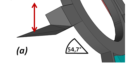
38 Calibration 54,7 40/68
39 AFM probe integration 41/68
40 Force resolution V AC +V DC Signal processing Measurement noise level: 7µV/ Hz Probe settings f 0 10,975MHz Q 1300 k e 180kN.m -1 HF measur ement Calibration: 5nm/V AC Scanner control Amplitude measurement resolution: 50fm/ Hz Force resolution: 5pN/ Hz 42/68 42
41 AFM images: 11MHz probe
 Sample: J.-M. Arbona, J.-P.")
42 AFM experiment: DNA origamis R ext 30 µm R int 10 µm th. 5 µm f MHz Q k eff 180 kn.m -1 Probe parameters f A 0 Scan size lin. Speed Time/frame MHz 0.2 nm 2 x 2 µm² 19 µm/s 55 s AFM images of DNA Origami on mica (real time) Sample: J.-M. Arbona, J.-P. Aimé, CBMN (Pessac) AFM parameters
43 DNA Origamis on Mica substrate Journée Trans GDR, 11 avril 2012 Besançon, 45/68 France
44 Height measurement Height
45 DNA Origami imaging: image capture
46 Conclusion: AFM experiment on DNA Origamis 1frame/second AFM imaging on DNA Origami No degradation of the bio-molecular structure Proof of concept paving the way for AFM MEMS Probe based of biological applications Z image Phase image Probe f 0 Q relax A min F min Cantilever 250 khz ms 1 pm.hz pn.hz -0.5 MEMS AFM 11 MHz µs 50 fm.hz pn.hz -0.5 Comparing the performance of AFM probes (at ambient pressure) Limitations: Cantilever: thermomechanical noise MEMS Probe: transduction efficiency + electronic noise
47 Y[µm] High frequency AFM: State of the art DNA origamis image done with a probe resonating at 18,4MHz nm 4 3 Settings 2 f 0 A 18,4MHz 0,1nm 1 Scan Size nb of lines x 5 µm² nm Lin Velocity 2µm/s X[µm] Samples: J.-M. Arbo, J.-P. Aimé, CBMN, Pessac 49/68
48 Conclusion - Outlook Amplitude noise <0.5pm/ Hz Phase noise <5m / Hz Force resolution < 10pN/ Hz Outlook High speed imaging is possible (video rate) Give access to real-time protein folding (origami) Piezoresistive sensing Piezoresistive actuation Journée Trans GDR, 11 avril 2012 Besançon, 50/68 France
 could be attained while vibrating in the elliptic mode.")
49 Outlook Piezoresistive detection The piezo-resistances (areas in black) are placed at the zone where the maximal deformation of the same kind (compression or extension) could be attained while vibrating in the elliptic mode. Journée Trans GDR, 11 avril 2012 Besançon, 51/68 France
50 «During MEMS 12, we had» Piezo resistive resonator Piezo-resistance access Excitation access Piezo-resistance access

51 Acknowledgements Fundings SMART Improve-LM Jean-Pierre Aimé, Jean-Michel Arbona, CBMN, Pessac Univ. Bordeaux Permanent staff: E. Algré, M. Faucher, B. Legrand, D. Théron Ph.D. student: B. Walter, Z. Xiong IEMN Laboratory technical staff M. Ozinski, C. Legrand, C. Boyaval, D. Troadec, V. Brandli D. Vandermoere, B. Laurent, D. Ducatteau, E. Mairiaux, Y. Desmedts 53/68
52 54/68
7/3/2014. Introduction to Atomic Force Microscope. Introduction to Scanning Force Microscope. Invention of Atomic Force Microscope (AFM)
") Introduction to Atomic Force Microscope Introduction to Scanning Force Microscope Not that kind of atomic Tien Ming Chuang ( 莊 天 明 ) Institute of Physics, Academia Sinica Tien Ming Chuang ( 莊 天 明 ) Institute
Introduction to Atomic Force Microscope Introduction to Scanning Force Microscope Not that kind of atomic Tien Ming Chuang ( 莊 天 明 ) Institute of Physics, Academia Sinica Tien Ming Chuang ( 莊 天 明 ) Institute
STM and AFM Tutorial. Katie Mitchell January 20, 2010
 STM and AFM Tutorial Katie Mitchell January 20, 2010 Overview Scanning Probe Microscopes Scanning Tunneling Microscopy (STM) Atomic Force Microscopy (AFM) Contact AFM Non-contact AFM RHK UHV350 AFM/STM
Scanning Near-Field Optical Microscopy for Measuring Materials Properties at the Nanoscale
 Scanning Near-Field Optical Microscopy for Measuring Materials Properties at the Nanoscale Outline Background Research Design Detection of Near-Field Signal Submonolayer Chemical Sensitivity Conclusions
Lecture 4 Scanning Probe Microscopy (SPM)
") Lecture 4 Scanning Probe Microscopy (SPM) General components of SPM; Tip --- the probe; Cantilever --- the indicator of the tip; Tip-sample interaction --- the feedback system; Scanner --- piezoelectric
Lecture 4 Scanning Probe Microscopy (SPM) General components of SPM; Tip --- the probe; Cantilever --- the indicator of the tip; Tip-sample interaction --- the feedback system; Scanner --- piezoelectric
Nano Meter Stepping Drive of Surface Acoustic Wave Motor
 Proc. of 1st IEEE Conf. on Nanotechnology, Oct. 28-3, pp. 495-5, (21) Maui, Hawaii Nano Meter Stepping Drive of Surface Acoustic Wave Motor Takashi Shigematsu*, Minoru Kuribayashi Kurosawa*, and Katsuhiko
1 Introduction. 1.1 Historical Perspective
 j1 1 Introduction 1.1 Historical Perspective The invention of scanning probe microscopy is considered one of the major advances in materials science since 1950 [1, 2]. Scanning probe microscopy includes
ENS 07 Paris, France, 3-4 December 2007
 ENS 7 Paris, France, 3-4 December 7 FRICTION DRIVE SIMULATION OF A SURFACE ACOUSTIC WAVE MOTOR BY NANO VIBRATION Minoru Kuribayashi Kurosawa, Takashi Shigematsu Tokyou Institute of Technology, Yokohama
Lecture 6 Scanning Tunneling Microscopy (STM) General components of STM; Tunneling current; Feedback system; Tip --- the probe.
 General components of STM; Tunneling current; Feedback system; Tip --- the probe.") Lecture 6 Scanning Tunneling Microscopy (STM) General components of STM; Tunneling current; Feedback system; Tip --- the probe. Brief Overview of STM Inventors of STM The Nobel Prize in Physics 1986 Nobel
Lecture 6 Scanning Tunneling Microscopy (STM) General components of STM; Tunneling current; Feedback system; Tip --- the probe. Brief Overview of STM Inventors of STM The Nobel Prize in Physics 1986 Nobel
Keysight Technologies How to Choose your MAC Lever. Technical Overview
 Keysight Technologies How to Choose your MAC Lever Technical Overview Introduction Atomic force microscopy (AFM) is a sub-nanometer scale imaging and measurement tool that can be used to determine a sample
NEAR FIELD OPTICAL MICROSCOPY AND SPECTROSCOPY WITH STM AND AFM PROBES
 Vol. 93 (1997) A CTA PHYSICA POLONICA A No. 2 Proceedings of the 1st International Symposium on Scanning Probe Spectroscopy and Related Methods, Poznań 1997 NEAR FIELD OPTICAL MICROSCOPY AND SPECTROSCOPY
Non-Contact Vibration Measurement of Micro-Structures
 Non-Contact Vibration Measurement of Micro-Structures Using Laser Doppler Vibrometry (LDV) and Planar Motion Analysis (PMA) to examine and assess the vibration characteristics of micro- and macro-structures.
A METHOD OF PRECISE CALIBRATION FOR PIEZOELECTRICAL ACTUATORS
 Uludağ Üniversitesi Mühendislik-Mimarlık Fakültesi Dergisi, Cilt 9, Sayı, 24 A METHOD OF PRECISE CALIBRATION FOR PIEZOELECTRICAL ACTUATORS Timur CANEL * Yüksel BEKTÖRE ** Abstract: Piezoelectrical actuators
19 th INTERNATIONAL CONGRESS ON ACOUSTICS MADRID, 2-7 SEPTEMBER 2007
 19 th INTERNATIONAL CONGRESS ON ACOUSTICS MADRID, 2-7 SEPTEMBER 2007 MICROMACHINED MICROPHONES WITH DIFFRACTION-BASED OPTICAL INTERFEROMETRIC READOUT AND ELECTROSTATIC ACTUATION PACS: 43.38.Ar F. Levent
MEMS mirror for low cost laser scanners. Ulrich Hofmann
 MEMS mirror for low cost laser scanners Ulrich Hofmann Outline Introduction Optical concept of the LIDAR laser scanner MEMS mirror requirements MEMS mirror concept, simulation and design fabrication process
Basic principles and mechanisms of NSOM; Different scanning modes and systems of NSOM; General applications and advantages of NSOM.
 Lecture 16: Near-field Scanning Optical Microscopy (NSOM) Background of NSOM; Basic principles and mechanisms of NSOM; Basic components of a NSOM; Different scanning modes and systems of NSOM; General
Development of New Inkjet Head Applying MEMS Technology and Thin Film Actuator
 Development of New Inkjet Head Applying MEMS Technology and Thin Film Actuator Kenji MAWATARI, Koich SAMESHIMA, Mitsuyoshi MIYAI, Shinya MATSUDA Abstract We developed a new inkjet head by applying MEMS
Surface Profilometry as a tool to Measure Thin Film Stress, A Practical Approach. Gianni Franceschinis, RIT MicroE Graduate Student
 1 Surface Profilometry as a tool to Measure Thin Film Stress, A Practical Approach. Gianni Franceschinis, RIT MicroE Graduate Student Abstract-- As the film decreases in thickness the requirements of more
SCS Directory Accreditation number: SCS 0115
 International standard: ISO/IEC 17025:2005 Swiss standard: SN EN ISO/IEC 17025:2005 METRON SA Calibration Laboratory Via Luserte Sud 7 CH-6572 Quartino Head: Angelo Capone Responsible for MS: Angelo Capone
Micro Power Generators. Sung Park Kelvin Yuk ECS 203
 Micro Power Generators Sung Park Kelvin Yuk ECS 203 Overview Why Micro Power Generators are becoming important Types of Micro Power Generators Power Generators Reviewed Ambient Vibrational energy Radiant
Microscopie à force atomique: Le mode noncontact
 Microscopie à force atomique: Le mode noncontact Clemens Barth barth@crmcn.univ-mrs.fr CRMCN-CNRS, Campus de Lumny, Case 913, 13288 Marseille Cedex09, France La Londe les Maures (France) -- 20-21/03/2007
5. Scanning Near-Field Optical Microscopy 5.1. Resolution of conventional optical microscopy
 5. Scanning Near-Field Optical Microscopy 5.1. Resolution of conventional optical microscopy Resolution of optical microscope is limited by diffraction. Light going through an aperture makes diffraction
Nanoceanal Spectroscopy of Vibrariums and Electariums
 FEM-Simulationen von Feldverteilungen im elektrischen Rasterkraft-Mikroskop Falk Müller 100 nm 2,93 nm 0 nm Experimental set-up Results Results on gold Application on silicon Numerical umerical simulations
III. MEMS Projection Helvetica 20 Displays
 Helvetica 26 Helvetica 22 III. MEMS Projection Displays Micro Mirror Projection - Texas Instruments DMD - Daewoo Elec. AMA Grating Light Valve - Silicon Light Machines Image Projection Color Synthesis
Le nanotecnologie: dal Laboratorio al Mercato. Fabrizio Pirri Politecnico di Torino Istituto Italiano di Tecnologia
 Le nanotecnologie: dal Laboratorio al Mercato Fabrizio Pirri Politecnico di Torino Istituto Italiano di Tecnologia Materials & Processes for micro nanotechnologies Laboratory http://www.polito.it/micronanotech
2004 Elsevier Science. Reprinted with permission from Elsevier.
 M. Koskenvuori, T. Mattila, A. Häärä, J. Kiihamäki, I. Tittonen, A. Oja, and H. Seppä, Long term stability of single crystal silicon microresonators, Sensors and Actuators A: Physical, 115, pp. 23 27 (24).
Laser-induced surface phonons and their excitation of nanostructures
 CHINESE JOURNAL OF PHYSICS VOL. 49, NO. 1 FEBRUARY 2011 Laser-induced surface phonons and their excitation of nanostructures Markus Schmotz, 1, Dominik Gollmer, 1 Florian Habel, 1 Stephen Riedel, 1 and
RF energy harvester based on MEMS
 9/9/010 NiPS Summer School 010 Summer School: Energy Harvesting at micro and nanoscale, August 1 6, 010 NiPSWorkshop: Noiseindynamicalsystemsat themicro and nanoscale, August6 8, 010 La Tenuta dei Ciclamini,
Tecniche a scansione di sonda per nanoscopia e nanomanipolazione 2: AFM e derivati
 LS Scienza dei Materiali - a.a. 2008/09 Fisica delle Nanotecnologie part 5.2 Version 7, Nov 2008 Francesco Fuso, tel 0502214305, 0502214293 - fuso@df.unipi.it http://www.df.unipi.it/~fuso/dida Tecniche
Traceable cantilever stiffness calibration method using a MEMS nano-force transducer
 Traceable cantilever stiffness calibration method using a MEMS nano-force transducer Sai Gao 1, Uwe Brand 1, Wolfgang Engl 2, Thomas Sulzbach 2 1 PTB, 5.11 Hardness and tactile probing methods 2 Nanoworld
Silicon-On-Glass MEMS. Design. Handbook
 Silicon-On-Glass MEMS Design Handbook A Process Module for a Multi-User Service Program A Michigan Nanofabrication Facility process at the University of Michigan March 2007 TABLE OF CONTENTS Chapter 1...
Self-Mixing Laser Diode Vibrometer with Wide Dynamic Range
 Self-Mixing Laser Diode Vibrometer with Wide Dynamic Range G. Giuliani,, S. Donati, L. Monti -, Italy Outline Conventional Laser vibrometry (LDV) Self-mixing interferometry Self-mixing vibrometer Principle:
Recent developments in high bandwidth optical interconnects. Brian Corbett. www.tyndall.ie
 Recent developments in high bandwidth optical interconnects Brian Corbett Outline Introduction to photonics for interconnections Polymeric waveguides and the Firefly project Silicon on insulator (SOI)
Single Protein Nanobiosensor. Grid Array (SPOT-NOSED)
") Single Protein Nanobiosensor Grid Array (SPOT-NOSED) Single Protein Nanobiosensor! Abstract Recent advances in bio- and nano-technology have opened the possibility to develop bio-electronic sensors based
Single Protein Nanobiosensor Grid Array (SPOT-NOSED) Single Protein Nanobiosensor! Abstract Recent advances in bio- and nano-technology have opened the possibility to develop bio-electronic sensors based
Scanning Probe Microscopy
 Ernst Meyer Hans Josef Hug Roland Bennewitz Scanning Probe Microscopy The Lab on a Tip With 117 Figures Mß Springer Contents 1 Introduction to Scanning Probe Microscopy f f.1 Overview 2 f.2 Basic Concepts
Calibration of AFM with virtual standards; robust, versatile and accurate. Richard Koops VSL Dutch Metrology Institute Delft
 Calibration of AFM with virtual standards; robust, versatile and accurate Richard Koops VSL Dutch Metrology Institute Delft 19-11-2015 VSL Dutch Metrology Institute VSL is the national metrology institute
ATOMIC FORCE MICROSCOPY
 ATOMIC FORCE MICROSCOPY Introduction The atomic force microscope, or AFM, is a member of the family of instruments known as scanning probe microscopes. The AFM operates under a completely different principle
Laboratorio Regionale LiCryL CNR-INFM
 Laboratorio Regionale LiCryL CNR-INFM c/o Physics Department - University of Calabria, Ponte P. Bucci, Cubo 33B, 87036 Rende (CS) Italy UNIVERSITÀ DELLA CALABRIA Dipartimento di FISICA Researchers Dr.
Piezoelectric Scanners
 Piezoelectric Scanners Piezoelectric materials are ceramics that change dimensions in response to an applied voltage and conversely, they develop an electrical potential in response to mechanical pressure.
nanovea.com MECHANICAL TESTERS Indentation Scratch Wear
 MECHANICAL TESTERS Indentation Scratch Wear nanovea.com MECHANICAL TESTER INTRO Nanovea Mechanical Testers provide unmatched multi-function Nano and Micro/Macro modules on a single platform. Both the Nano
Fast-scanning near-field scanning optical microscopy. using a high-frequency dithering probe
 Fast-scanning near-field scanning optical microscopy using a high-frequency dithering probe Yongho Seo and Wonho Jhe * Center for Near-field Atom-photon Technology and School of Physics, Seoul National
SCANNING PROBE MICROSCOPY NANOS-E3 SCHOOL 29/09/2015 An introduction to surface microscopy probes
 SCANNING PROBE MICROSCOPY NANOS-E3 SCHOOL 29/09/2015 An introduction to surface microscopy probes SPM is ubiquitous in modern research Physics Nanotechnology/chemistry Nature Nanotechnology 10, 156 160
Schedule of Accreditation issued by United Kingdom Accreditation Service 21-47 High Street, Feltham, Middlesex, TW13 4UN, UK
 code Location code Customers Sites locations: 21-47 High Street, Feltham, Middlesex, TW13 4UN, UK Calibration Centre Bolkiah Garrison BB3510 Negara Brunei Darussalam Contact: Mr Lim Tiong Thai Tel: +673-2-386475
Multi-mode Atomic Force Microscope (with High Voltage Piezo Force Microscope and +/- 8000 Oe Variable Field module.)
") Multi-mode Atomic Force Microscope (with High Voltage Piezo Force Microscope and +/- 8000 Oe Variable Field module.) Main specifications of the proposed instrument: 1 Instrument Resolution: 1.1 The instrument
Multi-mode Atomic Force Microscope (with High Voltage Piezo Force Microscope and +/- 8000 Oe Variable Field module.) Main specifications of the proposed instrument: 1 Instrument Resolution: 1.1 The instrument
Micro-Power Generation
 Micro-Power Generation Elizabeth K. Reilly February 21, 2007 TAC-meeting 1 Energy Scavenging for Wireless Sensors Enabling Wireless Sensor Networks: Ambient energy source Piezoelectric transducer technology
Chalmers Publication Library
 Chalmers Publication Library Contactless pin-flange adapter for high-frequency measurements This document has been downloaded from Chalmers Publication Library (CPL). It is the author s version of a work
Microscopie à champs proche: et application
 Microscopie à champs proche: Théorie et application STM, effet tunnel et applications AFM, interactions et applications im2np, Giens 2010 Optical microscopy: resolution limit resolution limit: d min =
RX-AM4SF Receiver. Pin-out. Connections
 RX-AM4SF Receiver The super-heterodyne receiver RX-AM4SF can provide a RSSI output indicating the amplitude of the received signal: this output can be used to create a field-strength meter capable to indicate
Nano-Spectroscopy. Solutions AFM-Raman, TERS, NSOM Chemical imaging at the nanoscale
 Nano-Spectroscopy Solutions AFM-Raman, TERS, NSOM Chemical imaging at the nanoscale Since its introduction in the early 80 s, Scanning Probe Microscopy (SPM) has quickly made nanoscale imaging an affordable
MEMS Processes from CMP
 MEMS Processes from CMP MUMPS from MEMSCAP Bulk Micromachining 1 / 19 MEMSCAP MUMPS processes PolyMUMPS SOIMUMPS MetalMUMPS 2 / 19 MEMSCAP Standard Processes PolyMUMPs 8 lithography levels, 7 physical
DATA SHEET. TDA1518BQ 24 W BTL or 2 x 12 watt stereo car radio power amplifier INTEGRATED CIRCUITS
 INTEGRATED CIRCUITS DATA SHEET File under Integrated Circuits, IC01 July 1994 GENERAL DESCRIPTION The is an integrated class-b output amplifier in a 13-lead single-in-line (SIL) plastic power package.
From apertureless near-field optical microscopy to infrared near-field night vision
 From apertureless near-field optical microscopy to infrared near-field night vision Yannick DE WILDE ESPCI Laboratoire d Optique Physique UPR A0005-CNRS, PARIS dewilde@optique.espci.fr From apertureless
An Electromagnetic Micro Power Generator Based on Mechanical Frequency Up-Conversion
 International Journal of Materials Science and Engineering Vol. 1, No. December 013 An Electromagnetic Micro Power Generator Based on Mechanical Frequency Up-Conversion Vida Pashaei and Manouchehr Bahrami
Injection moulding and modelling on a micro scale
 Injection moulding and modelling on a micro scale Technology Update Injection moulding and welding of plastics 11 November 2014 Research Projects (National / European) Micro/Nano/Multimaterial Manufacturing
INTEGRATED CIRCUITS DATA SHEET. TDA7000 FM radio circuit. Product specification File under Integrated Circuits, IC01
 INTEGRATED CIRCUITS DATA SHEET File under Integrated Circuits, IC01 May 1992 GENERAL DESCRIPTION The is a monolithic integrated circuit for mono FM portable radios, where a minimum on peripheral components
Case Study 2: Digital Micromirror Devices (DMD) Optical MEMS
 Optical MEMS") Case Study : Digital Micromirror Devices (DMD) Chapter of Senturia A MEMS-based projection display, Van Kessel, P.F.; Hornbeck, L.J.; Meier, R.E.; Douglass, M.R., Proc. IEEE, Vol. 86 pp.1687-174 1998 http://www.dlp.com/
Case Study : Digital Micromirror Devices (DMD) Chapter of Senturia A MEMS-based projection display, Van Kessel, P.F.; Hornbeck, L.J.; Meier, R.E.; Douglass, M.R., Proc. IEEE, Vol. 86 pp.1687-174 1998 http://www.dlp.com/
Combined atomic force microscope and acoustic wave devices: application to electrodeposition.
 Combined atomic force microscope and acoustic wave devices: application to electrodeposition. J.-M. Friedt, L. Francis, K.-H. Choi, F. Frederix and A. Campitelli friedtj@imec.be, campi@imec.be October
RF data receiver super-reactive ASK modulation, low cost and low consumption ideal for Microchip HCS KEELOQ decoder/encoder family. 0.
 Receiver AC-RX2/CS RF data receiver super-reactive ASK modulation, low cost and low consumption ideal for Microchip HCS KEELOQ decoder/encoder family. Pin-out 38.1 3 Component Side 1 2 3 7 11 13 14 15
Microstockage d énergie Les dernières avancées. S. Martin (CEA-LITEN / LCMS Grenoble)
") Microstockage d énergie Les dernières avancées S. Martin (CEA-LITEN / LCMS Grenoble) 1 Outline What is a microbattery? Microbatteries developped at CEA Description Performances Integration and Demonstrations
Microstockage d énergie Les dernières avancées S. Martin (CEA-LITEN / LCMS Grenoble) 1 Outline What is a microbattery? Microbatteries developped at CEA Description Performances Integration and Demonstrations
Nanoscale Resolution Options for Optical Localization Techniques. C. Boit TU Berlin Chair of Semiconductor Devices
 berlin Nanoscale Resolution Options for Optical Localization Techniques C. Boit TU Berlin Chair of Semiconductor Devices EUFANET Workshop on Optical Localization Techniques Toulouse, Jan 26, 2009 Jan 26,
NP-AFM. Samples as large as 200 x 200 x 20 mm are profiled by the NP-AFM system, and several stage options are available for many types of samples.
 NP-AFM The NP-AFM is a complete nanoprofiler tool including everything required for scanning samples: microscope stage, electronic box, control computer, probes, manuals, and a video microscope. Samples
Spin-flip excitation spectroscopy with STM excitation of allowed transition adds an inelastic contribution (group of Andreas Heinrich, IBM Almaden)
") Magnetism at the atomic scale by Scanning Probe Techniques Kirsten von Bergmann Institute of Applied Physics Magnetism with SPM Spin-polarized scanning tunneling microscopy SP-STM density of states of
Magnetism at the atomic scale by Scanning Probe Techniques Kirsten von Bergmann Institute of Applied Physics Magnetism with SPM Spin-polarized scanning tunneling microscopy SP-STM density of states of
INTRODUCTION TO SCANNING TUNNELING MICROSCOPY
 INTRODUCTION TO SCANNING TUNNELING MICROSCOPY SECOND EDITION C. JULIAN CHEN Department of Applied Physics and Applied Mathematics, Columbia University, New York OXJORD UNIVERSITY PRESS Contents Preface
MATRIX TECHNICAL NOTES
 200 WOOD AVENUE, MIDDLESEX, NJ 08846 PHONE (732) 469-9510 FAX (732) 469-0418 MATRIX TECHNICAL NOTES MTN-107 TEST SETUP FOR THE MEASUREMENT OF X-MOD, CTB, AND CSO USING A MEAN SQUARE CIRCUIT AS A DETECTOR
PowerAmp Design. PowerAmp Design PAD135 COMPACT HIGH VOLATGE OP AMP
 PowerAmp Design COMPACT HIGH VOLTAGE OP AMP Rev G KEY FEATURES LOW COST SMALL SIZE 40mm SQUARE HIGH VOLTAGE 200 VOLTS HIGH OUTPUT CURRENT 10A PEAK 40 WATT DISSIPATION CAPABILITY 200V/µS SLEW RATE APPLICATIONS
Supertex inc. HV256. 32-Channel High Voltage Amplifier Array HV256. Features. General Description. Applications. Typical Application Circuit
 32-Channel High Voltage Amplifier Array Features 32 independent high voltage amplifiers 3V operating voltage 295V output voltage 2.2V/µs typical output slew rate Adjustable output current source limit
Piezoelectric Driven Non-toxic Injector for Automated Cell Manipulation
 Medicine Meets Virtual Reality 18 J.D. Westwood et al. (Eds.) IOS Press, 2011 2011 The authors. All rights reserved. doi:10.3233/978-1-60750-706-2-231 231 Piezoelectric Driven Non-toxic Injector for Automated
E_mail: afmproject@free.fr
 Décines - France Student team : PORCHER Nicolas ROMEU Guillaume TISSOT François Teacher : JEANJACQUOT Philippe E_mail: afmproject@free.fr Picture gallery 2 Summary A nanometric picture for a nanometric
The Design and Characteristic Study of a 3-dimensional Piezoelectric Nano-positioner
 SICE Annual Conference August 8-,, The Grand Hotel, Taipei, Taiwan The Design and Characteristic Study of a -dimensional Piezoelectric Nano-positioner Yu-Chi Wang Department of Mechanical Engineering National
It has long been a goal to achieve higher spatial resolution in optical imaging and
 Nano-optical Imaging using Scattering Scanning Near-field Optical Microscopy Fehmi Yasin, Advisor: Dr. Markus Raschke, Post-doc: Dr. Gregory Andreev, Graduate Student: Benjamin Pollard Department of Physics,
A. Ricci, E. Giuri. Materials and Microsystems Laboratory
 Presented at the COMSOL Conference 2009 Milan FSI Analysis of Microcantilevers Vibrating in Fluid Environment Materials and Microsystems Laboratory Politecnico di Torino Outline Brief Presentation of Materials
PS25202 EPIC Ultra High Impedance ECG Sensor Advance Information
 EPIC Ultra High Impedance ECG Sensor Advance Information Data Sheet 291498 issue 2 FEATURES Ultra high input resistance, typically 20GΩ. Dry-contact capacitive coupling. Input capacitance as low as 15pF.
How to measure absolute pressure using piezoresistive sensing elements
 In sensor technology several different methods are used to measure pressure. It is usually differentiated between the measurement of relative, differential, and absolute pressure. The following article
How To Use A Sound Card With A Subsonic Sound Card
 !"## $#!%!"# &"#' ( "#' )*! #+ #,# "##!$ -+./0 1" 1! 2"# # -&1!"#" (2345-&1 #$6.7 -&89$## ' 6! #* #!"#" +" 1##6$ "#+# #-& :1# # $ #$#;1)+#1#+
BIOMEDICAL ULTRASOUND
 BIOMEDICAL ULTRASOUND Goals: To become familiar with: Ultrasound wave Wave propagation and Scattering Mechanisms of Tissue Damage Biomedical Ultrasound Transducers Biomedical Ultrasound Imaging Ultrasonic
DATA SHEET. TDA8560Q 2 40 W/2 Ω stereo BTL car radio power amplifier with diagnostic facility INTEGRATED CIRCUITS. 1996 Jan 08
 INTEGRATED CIRCUITS DATA SHEET power amplifier with diagnostic facility Supersedes data of March 1994 File under Integrated Circuits, IC01 1996 Jan 08 FEATURES Requires very few external components High
Copyright 2015 ASM International.
 Copyright 2015 ASM International. This paper was published in Electronic Device Failure Analysis, Vol. 17, Issue 3, pp. 4-6, 8-10 and is made available as an electronic reprint with the permission of ASM
Electromouillage réversible sur nanofils de silicium superhydrophobes
 Electromouillage réversible sur nanofils de silicium superhydrophobes EWOD: Electro Wetting On Dielectrics Rabah Boukherroub 1,2 N. Verplanck, 2 G.Piret 1,2 Y. Coffinier, 1,2 E. Galopin, 2 V. Thomy, 2
NI USB-5681 RF Power Meter Specifications
 NI USB-568 RF Power Meter Specifications General This document lists specifications for the NI USB-568 RF power meter. Minimum or maximum specifications are warranted under the following conditions: hour
Emerging new non conventional tools
 Emerging new non conventional tools Near field lithography Near field lithography Near field lithography through local electrochemistry example of gold a) Surface water condensation b) Monolayer of oxidized
Nano Optics: Overview of Research Activities. Sergey I. Bozhevolnyi SENSE, University of Southern Denmark, Odense, DENMARK
 Nano Optics: Overview of Research Activities SENSE, University of Southern Denmark, Odense, DENMARK Optical characterization techniques: Leakage Radiation Microscopy Scanning Near-Field Optical Microscopy
THERMAL ANEMOMETRY ELECTRONICS, SOFTWARE AND ACCESSORIES
 TSI and TSI logo are registered trademarks of TSI Incorporated. SmartTune is a trademark of TSI Incorporated. THERMAL ANEMOMETRY ELECTRONICS, SOFTWARE AND ACCESSORIES IFA 300 Constant Temperature Anemometry
SFP-SX with DOM 1.25Gb/s Multi-Mode SFP Transceiver 1000BASE-SX 1.0625Gb/s Fiber Channel
 Product Features Compliant to IEEE Std 802.3-2005 Gigabit Ethernet 1000Base-SX, with DOM Specifications according to SFF-8074i and SFF-8472, revision 9.5 Digital Diagnostic Monitoring 850nm Vertical Cavity
Towards a miniaturized micromechanical electronic nose SYWERT H. BRONGERSMA SR. PRINCIPAL RESEARCHER
 Towards a miniaturized micromechanical electronic nose SYWERT H. BRONGERSMA SR. PRINCIPAL RESEARCHER e-nose: advanced sensing in complex environments Human olfactory system e-nose: array of non-specific,
Leti Introduction and Overview
 Leti Introduction and Overview Leti Day in Tokyo, October 3rd 2012 Laurent Malier 2012 Leti 2012 1 CEA The CEA at a glance Commissariat à l Énergie Atomique et aux Énergies Alternatives is one of the largest
Photolithography. Class: Figure 12.1. Various ways in which dust particles can interfere with photomask patterns.
 Photolithography Figure 12.1. Various ways in which dust particles can interfere with photomask patterns. 19/11/2003 Ettore Vittone- Fisica dei Semiconduttori - Lectio XIII 16 Figure 12.2. Particle-size
CREOL, College of Optics & Photonics, University of Central Florida
 OSE6650 - Optical Properties of Nanostructured Materials Optical Properties of Nanostructured Materials Fall 2013 Class 3 slide 1 Challenge: excite and detect the near field Thus far: Nanostructured materials
Compact mobilized and low-cost scanning tunneling microscope for educational use
 A. Compact mobilized and low-cost scanning tunneling microscope for educational use Eli Flaxer AFEKA - Tel-Aviv Academic College of Engineering, 69107 Tel-Aviv, Israel. We developed a mobile, compact and
Technical Datasheet Scalar Network Analyzer Model 8003-10 MHz to 40 GHz
 Technical Datasheet Scalar Network Analyzer Model 8003-10 MHz to 40 GHz The Giga-tronics Model 8003 Precision Scalar Network Analyzer combines a 90 db wide dynamic range with the accuracy and linearity
4 SENSORS. Example. A force of 1 N is exerted on a PZT5A disc of diameter 10 mm and thickness 1 mm. The resulting mechanical stress is:
 4 SENSORS The modern technical world demands the availability of sensors to measure and convert a variety of physical quantities into electrical signals. These signals can then be fed into data processing
Characterization of surfaces by AFM topographical, mechanical and chemical properties
 Characterization of surfaces by AFM topographical, mechanical and chemical properties Jouko Peltonen Department of physical chemistry Åbo Akademi University Atomic Force Microscopy (AFM) Contact mode AFM
Overview of Energy Harvesting Systems (for low-power electronics)
") Overview of Energy Harvesting Systems (for low-power electronics) Gyuhae Park Engineering Institute Engineering Sciences & Applications Los Alamos National Laboratory The First Engineering Institute Workshop:
Overview of Energy Harvesting Systems (for low-power electronics) Gyuhae Park Engineering Institute Engineering Sciences & Applications Los Alamos National Laboratory The First Engineering Institute Workshop:
Self-Mixing Differential Laser Vibrometer
 Self-Mixing Differential Laser Vibrometer Michele Norgia e Informazione, Politecnico di Milano, Italy Guido Giuliani,, Silvano Donati -,, Italy guido.giuliani@unipv.it Outline Conventional Laser Doppler
MRF175GU MRF175GV The RF MOSFET Line 200/150W, 500MHz, 28V
 Designed for broadband commercial and military applications using push pull circuits at frequencies to 500 MHz. The high power, high gain and broadband performance of these devices makes possible solid
Scanning Near Field Optical Microscopy: Principle, Instrumentation and Applications
 Scanning Near Field Optical Microscopy: Principle, Instrumentation and Applications Saulius Marcinkevičius Optics, ICT, KTH 1 Outline Optical near field. Principle of scanning near field optical microscope
Making Accurate Voltage Noise and Current Noise Measurements on Operational Amplifiers Down to 0.1Hz
 Author: Don LaFontaine Making Accurate Voltage Noise and Current Noise Measurements on Operational Amplifiers Down to 0.1Hz Abstract Making accurate voltage and current noise measurements on op amps in
- particle with kinetic energy E strikes a barrier with height U 0 > E and width L. - classically the particle cannot overcome the barrier
 Tunnel Effect: - particle with kinetic energy E strikes a barrier with height U 0 > E and width L - classically the particle cannot overcome the barrier - quantum mechanically the particle can penetrated
CONCEPT OF DETERMINISTIC ION IMPLANTATION AT THE NANOSCALE
 CONCEPT OF DETERMINISTIC ION IMPLANTATION AT THE NANOSCALE Daniel Spemann Jan Meijer 1, Jürgen W. Gerlach, Paul Räcke 1, Susann Liedtke, Stephan Rauschenbach 2, Bernd Rauschenbach 1 University of Leipzig,
Measuring Temperature withthermistors a Tutorial David Potter
 NATIONAL INSTRUMENTS The Software is the Instrument Application Note 065 Measuring Temperature withthermistors a Tutorial David Potter Introduction Thermistors are thermally sensitive resistors used in
Usage of Carbon Nanotubes in Scanning Probe Microscopes as Probe. Keywords: Carbon Nanotube, Scanning Probe Microscope
 International Journal of Arts and Sciences 3(1): 18-26 (2009) CD-ROM. ISSN: 1944-6934 InternationalJournal.org Usage of Carbon Nanotubes in Scanning Probe Microscopes as Probe Bedri Onur Kucukyildirim,
Innovative Wafer and Interconnect Technologies - Enabling High Volume Low Cost RFID Solutions
 Innovative Wafer and Interconnect Technologies - Enabling High Volume Low Cost RFID Solutions Innovative Wafer & Interconnect Technologies Outline Low cost RFID Tags & Labels Standard applications and