ENGINEERING EXPERIMENT STATION COLLEGE OF ENGINEERING THE UNIVERSITY OF ARIZONA TUCSON, ARIZONA USE OF A THREE-LAYER DISTRIBUTED RC NETWORK
|
|
|
- Camilla Horton
- 8 years ago
- Views:
Transcription
1 USE OF A THREE-LAYER DISTRIBUTED RC NETWORK TO PRODUCE TWO PAIRS OF COMPLEX CONJUGATE ZEROS Prepared under Grant NGL for the Instrumentation Division Ames Research Center Naional Aeronautics and Space Administration by L. P. Hue 1 sman ENGINEERING EXPERIMENT STATION COLLEGE OF ENGINEERING THE UNIVERSITY OF ARIZONA TUCSON, ARIZONA

2 'USE OF A THREE-LAYER DISTRIBUTED RC NETWORK TO PRODUCE TWO PAIRS OF COMPLEX CONJUGATE ZEROS Prepared under Grant NGL for the Instrumentation Division of the Ames Research Center National Aeronautics and Space Administration by L. P. Huelsman Department of Electrical Engineering University of Arizona Tucson, Arizona Abstract; This report describes the properties of a three-layer distributed RC network consisting of two layers of resistive material separated by a dielectric. When the three-layer network is used as a three-terminal element by connecting conducting terminal strips across the ends of one of the resistive layers and the center of the other resistive layer, the network may be used to produce pairs of complex conjugate transmission zeros. The locations of these zeros are determined by the parameters of the network. Design charts for determining the" zero positions are included as part of the report. January 1972

3 Use of a Three-Layer Distributed RC Network to Produce Two Pairs of Complex Conjugate Zeros I. Introduction '. This is one of a series of reports describing the use of digital computational techniques in the analysis and synthesis of DLA (Distributed-Lumped-Active) networks. This class of networks consists of three distinct types of elements, namely, distributed elements (modeled by partial differential equations), lumped elements (modeled by algebraic relations and ordinary differential equations), and active elements (modeled by algebraic relations)o Such a characterization is applicable to a bro-ad class of circuits, especially including those usually referred to as linear integrated circuits, since the fabrication techniques for such circuits readily produce elements which may be modeled as distributed, as well as the more conventional lumped and active ones. The network functions which describe distributed elements, "i however, involve hyperbolic irrational functions of the complex frequency variable. The complexity* of such functions make the use of digital computational techniques most desirable in analyzing and synthesizing these networks. ' In this report we shall consider the application of such digital computational techniques to the analysis and synthesis of a three-layer distributed RC network element. This element was first shown in a previous report to have the capabilities of
, and active elements (modeled by algebraic relations)o Such a characterization is applicable to a bro-ad class of circuits, especially including those usually")
4 producing a pair of transmission zeros on the jw axis. In this report we shall extend the previous results to show that the transmission zeros produced by the three-layer netv/ork may be located anywhere in the complex frequency plane. In addition, a series of design charts is given showing the locations of those zeros. II. The Three-Layer Distributed RC Network ' A three-layer uniform distributed-rc network, as analyzed in this report, consists of two layers of resistive material separated by a layer of dielectric material. As shown in Fig. 1, such a network may be considered as a three-terminal network element by adding three conducting terminal strips, two across the ends of one of the resistive layers, and one across the mid-region of the other resistive layer. The network may be characterized schematically as shown in Fig. 2, in which R is the total resistance of the resistive layer with two terminals, NR (where N is a positive constant of proportionality) is the total resistance that is measured between the ends of the resistive layer with the single terminal (if terminal strips were provided at the ends), and C is the total capacitance that exists between the two resistive layers. Because of the assumption that the distributed resistance and capacitance are uniform, i.e., R and C are constant rather than being functions of position, the network shown in Fig. 2 may be modeled as a cascade connection of two uniform distributed RC networks connected in cascade as shown in Fig. 3. In this figure, the

5 , x^ o- I /../\ RESISTIVE LAYER / DIELECTRIC LAYER RESISTIVE LAYER FIG. I R «>j 'vvvvvvvvvvv,..,.. - AVWv VWV\r w I, -{- V r\ ' 63 FIG. 2 o AVWVi. V 2 KNR r_ r\. FIG. 3 (I-K)R Is^> -..^A A A A i*- IL.II....1*^ ^fvv VV VJ (I~I\)C.1. AV\./«/v-. V, 1 N(I-K)R J
R Is^> -..^A A A A i*- IL.")
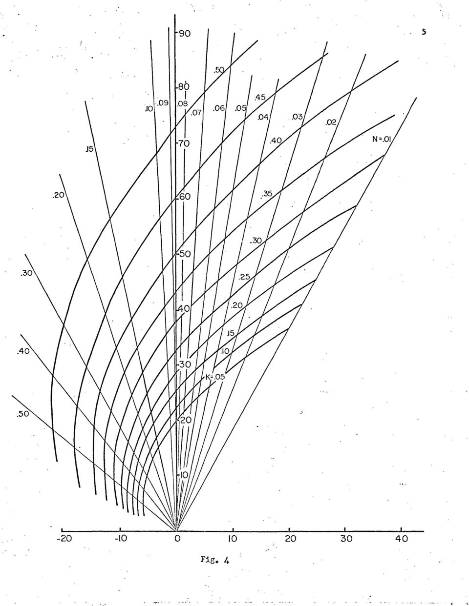
6 constant K has been defined to indicate the relative position of the terminal strip on the single-terminal resistive layer. For example, for K equals zero, the terminal strip is at the left end of the network shown in Fig. 1, and for K equals unity, it is at the right end. The voltage transfer function for this network may be shown to be :". V 2 " sinhk6 (NcoshK9 + 1) (NcoshMS + 1). V sinhq l~ 2 sinhki. / M 2... VVAJ-OM! sinhms,. VQ.,v2 - ^ I NK8 Q + (N +l)coshko+2n - -g (NcoshK.6+1) where 6 = \/prc(n+l), p is the complex frequency variable, and M=1-K. If N is set to the value ,.then transmission zeros are produced on the Jw axis, the relative locations of these zeros being determined by the value of K. III. Complex Conjugate Transmission Zeros Now let us consider the effect of using values of N other than the one specified in the preceding section. Choosing a range of values of N from 0.01 to 0.5 and a range of values of K from 0.05 to 0.5, and applying digital computational techniques similar to those described in the previous report, we obtain the charts shown in Figs. A and 5. Specifically Fig. A shows upper half-plane location of the lower complex.conjugate transmission zero of the network as a function of K and N, and Fig. 5 shows the upper halfplane location of the upper complex conjugate zero. Different scales are used for the two figures, however, the curve for K=0.5,
coshko+2n - -g (NcoshK.6+1) where 6 = \/prc(n+l), p is the complex frequency variable, and M=1-K. If N is set to the value 0.086266738,.")
7 Fig.
8 Fig. 5

9 F - representing the condition when the two complex-conjugate zeros are coincident and thus form a pair of second-order complex conjugate zeros, is shown on both figures to provide a common reference. IV. Applications There are two main applications which may be made of the complex conjugate zeros produced by the three-layer distributed RC network. First of all, we note that for K=0.5, a second-order pair of dominant complex conjugate zeros are produced. Thus, for such a value of K, this network is capable of producing rejection characteristics x^hich are more sharply defined than networks which have only a first order dominant complex conjugate transmission zero, such as the Kaufmann and Garrett lump-distributed RC notch 2 network. To illustrate this in Fig. 6, we show reciprocal sinusoidal steady-state characteristics for the transmission curves for the three-layer network (K=0.5) and the Kaufman and Garrett network. The 4 rad/sec and 8 rad/sec bandwidths for each of these networks is shown on the plot. For the three-layer network, there is approximately 10.5 db between these two bandwidths, while for the Kaufman and Garrett network there is only about 5 db. The improvement in selectivity made by the second-order zeros of the three-layer network is clearly evident. A second application which may be made for the three-layer distributed RC network is as a poledetermining element in a feedback loop around some active device.

10 ' 70" " 40" 30-8 r/s Kaufman and Garrett rad/sec Fig. 6

11 "Page missing from available version"

12 10 In such an application the transmission zeros of the distributed RC network become the poles of the overall network transfer function. As an example of the potentialities of the distributed RC network in producing a broad-band amplifier, response curves of the reciprocal of the voltage transfer function for N = 0.1, and for a range of values of K are shown in Fig. 7. the resonant peak due to the separation of the The broadening of complex-conjugate zeros of transmission is readily evident. ; V. Conclusion. In this report we have indicated the potential of the threelayer distributed RC network for producing complex-conjugate transmission zeros. The use of other degrees of freedom of the network in determining the location of such zeros, such as appropriately tapering the distributed RC element, is currently under study. A ckn ow1e d^men t s The support of this research by the Instrumentation Division of the Ames Research Center, National Aeronautics and Space Administration under Grant NGL is most gratefully acknowledged. The author would also like to express his appreciation to Mr. S. Raghunath for performing the programming associated with the development of the data used to draw some of the graphs.

13 11 db K = rod/see Fig. 7

14 12 References : 1. L. P. Huelsman, A Three-Layer Distributed RC Network with Two Transmission Zeros, University of Arizona Engineering Experiment Station Report, prepared under Grant NGL , 18 pages, Oct W. M. Kaufman and S. J. Garrett, Tapered Distributed Filters, IRE Trans. Circuit Theory, vol. CT-S, no. A, pp , Dec

Understanding Power Impedance Supply for Optimum Decoupling
 Introduction Noise in power supplies is not only caused by the power supply itself, but also the load s interaction with the power supply (i.e. dynamic loads, switching, etc.). To lower load induced noise,
Frequency Response of Filters
 School of Engineering Department of Electrical and Computer Engineering 332:224 Principles of Electrical Engineering II Laboratory Experiment 2 Frequency Response of Filters 1 Introduction Objectives To
2.161 Signal Processing: Continuous and Discrete Fall 2008
 MT OpenCourseWare http://ocw.mit.edu.6 Signal Processing: Continuous and Discrete Fall 00 For information about citing these materials or our Terms of Use, visit: http://ocw.mit.edu/terms. MASSACHUSETTS
Laboratory 4: Feedback and Compensation
 Laboratory 4: Feedback and Compensation To be performed during Week 9 (Oct. 20-24) and Week 10 (Oct. 27-31) Due Week 11 (Nov. 3-7) 1 Pre-Lab This Pre-Lab should be completed before attending your regular
Lab #9: AC Steady State Analysis
 Theory & Introduction Lab #9: AC Steady State Analysis Goals for Lab #9 The main goal for lab 9 is to make the students familar with AC steady state analysis, db scale and the NI ELVIS frequency analyzer.
OPERATIONAL AMPLIFIERS. o/p
 OPERATIONAL AMPLIFIERS 1. If the input to the circuit of figure is a sine wave the output will be i/p o/p a. A half wave rectified sine wave b. A fullwave rectified sine wave c. A triangular wave d. A
Sophomore Physics Laboratory (PH005/105)
") CALIFORNIA INSTITUTE OF TECHNOLOGY PHYSICS MATHEMATICS AND ASTRONOMY DIVISION Sophomore Physics Laboratory (PH5/15) Analog Electronics Active Filters Copyright c Virgínio de Oliveira Sannibale, 23 (Revision
CALIFORNIA INSTITUTE OF TECHNOLOGY PHYSICS MATHEMATICS AND ASTRONOMY DIVISION Sophomore Physics Laboratory (PH5/15) Analog Electronics Active Filters Copyright c Virgínio de Oliveira Sannibale, 23 (Revision
! #! % & % ( )! & +,,.! / 0 1 /) ) %222 3 4 1 5 6. /,,, %778,,9 / 6, : 0 9, 99, 3 +,, 9 9
! & +,,.! / 0 1 /) ) %222 3 4 1 5 6. /,,, %778,,9 / 6, : 0 9, 99, 3 +,, 9 9") ! #! % & % ( )! & +,,.! / 0 1 /) ) %222 3 4 1 5 6. /,,, %778,,9 / 6, : 0 9, 99, 3 +,, 9 9 ; 896 IEEE TRANSACTIONS ON MICROWAVE THEORY AND TECHNIQUES, VOL. 56, NO. 4, APRIL 2008 A Circuit-Theoretic Approach
! #! % & % ( )! & +,,.! / 0 1 /) ) %222 3 4 1 5 6. /,,, %778,,9 / 6, : 0 9, 99, 3 +,, 9 9 ; 896 IEEE TRANSACTIONS ON MICROWAVE THEORY AND TECHNIQUES, VOL. 56, NO. 4, APRIL 2008 A Circuit-Theoretic Approach
APPLICATION BULLETIN
 APPLICATION BULLETIN Mailing Address: PO Box 11400, Tucson, AZ 85734 Street Address: 6730 S. Tucson Blvd., Tucson, AZ 85706 Tel: (520) 746-1111 Telex: 066-6491 FAX (520) 889-1510 Product Info: (800) 548-6132
Understanding Poles and Zeros
 MASSACHUSETTS INSTITUTE OF TECHNOLOGY DEPARTMENT OF MECHANICAL ENGINEERING 2.14 Analysis and Design of Feedback Control Systems Understanding Poles and Zeros 1 System Poles and Zeros The transfer function
VCO K 0 /S K 0 is tho slope of the oscillator frequency to voltage characteristic in rads per sec. per volt.
 Phase locked loop fundamentals The basic form of a phase locked loop (PLL) consists of a voltage controlled oscillator (VCO), a phase detector (PD), and a filter. In its more general form (Figure 1), the
Analysis of Common-Collector Colpitts Oscillator
 Analysis of Common-Collector Colpitts Oscillator H R Pota May 20, 2005 Introduction Murphy s rule when paraphrased for oscillators reads [], Amplifiers will oscillate but oscillators won t. As we all know,
CHAPTER 6 Frequency Response, Bode Plots, and Resonance
 ELECTRICAL CHAPTER 6 Frequency Response, Bode Plots, and Resonance 1. State the fundamental concepts of Fourier analysis. 2. Determine the output of a filter for a given input consisting of sinusoidal
ISSCC 2003 / SESSION 10 / HIGH SPEED BUILDING BLOCKS / PAPER 10.5
 ISSCC 2003 / SESSION 10 / HIGH SPEED BUILDING BLOCKS / PAPER 10.5 10.5 Broadband ESD Protection Circuits in CMOS Technology Sherif Galal, Behzad Razavi Electrical Engineering Department, University of
Design of a TL431-Based Controller for a Flyback Converter
 Design of a TL431-Based Controller for a Flyback Converter Dr. John Schönberger Plexim GmbH Technoparkstrasse 1 8005 Zürich 1 Introduction The TL431 is a reference voltage source that is commonly used
Designing Stable Compensation Networks for Single Phase Voltage Mode Buck Regulators
 Designing Stable Compensation Networks for Single Phase Voltage Mode Buck Regulators Technical Brief December 3 TB47. Author: Doug Mattingly Assumptions This Technical Brief makes the following assumptions:.
Making Accurate Voltage Noise and Current Noise Measurements on Operational Amplifiers Down to 0.1Hz
 Author: Don LaFontaine Making Accurate Voltage Noise and Current Noise Measurements on Operational Amplifiers Down to 0.1Hz Abstract Making accurate voltage and current noise measurements on op amps in
Circuits with inductors and alternating currents. Chapter 20 #45, 46, 47, 49
 Circuits with inductors and alternating currents Chapter 20 #45, 46, 47, 49 RL circuits Ch. 20 (last section) Symbol for inductor looks like a spring. An inductor is a circuit element that has a large
SCHWEITZER ENGINEERING LABORATORIES, COMERCIAL LTDA.
 Pocket book of Electrical Engineering Formulas Content 1. Elementary Algebra and Geometry 1. Fundamental Properties (real numbers) 1 2. Exponents 2 3. Fractional Exponents 2 4. Irrational Exponents 2 5.
SERIES-PARALLEL DC CIRCUITS
 Name: Date: Course and Section: Instructor: EXPERIMENT 1 SERIES-PARALLEL DC CIRCUITS OBJECTIVES 1. Test the theoretical analysis of series-parallel networks through direct measurements. 2. Improve skills
ε: Voltage output of Signal Generator (also called the Source voltage or Applied
 Experiment #10: LR & RC Circuits Frequency Response EQUIPMENT NEEDED Science Workshop Interface Power Amplifier (2) Voltage Sensor graph paper (optional) (3) Patch Cords Decade resistor, capacitor, and
CHAPTER4 GENERAL ASPECTS OF MUTUAL
 CHAPTER4 GENERAL ASPECTS OF MUTUAL ADMITTANCE OF CPW-FED TWIN SLOTS ON CONDUCTOR-BACKED TWO-LAYER SUBSTRATES 4.1 INTRODUCTORY REMARKS The present chapter is concerned with an exploratory investigation
Positive Feedback and Oscillators
 Physics 3330 Experiment #6 Fall 1999 Positive Feedback and Oscillators Purpose In this experiment we will study how spontaneous oscillations may be caused by positive feedback. You will construct an active
Engineering Sciences 22 Systems Summer 2004
 Engineering Sciences 22 Systems Summer 24 BODE PLOTS A Bode plot is a standard format for plotting frequency response of LTI systems. Becoming familiar with this format is useful because: 1. It is a standard
Use and Application of Output Limiting Amplifiers (HFA1115, HFA1130, HFA1135)
") Use and Application of Output Limiting Amplifiers (HFA111, HFA110, HFA11) Application Note November 1996 AN96 Introduction Amplifiers with internal voltage clamps, also known as limiting amplifiers, have
Use and Application of Output Limiting Amplifiers (HFA111, HFA110, HFA11) Application Note November 1996 AN96 Introduction Amplifiers with internal voltage clamps, also known as limiting amplifiers, have
Chapter 12: The Operational Amplifier
 Chapter 12: The Operational Amplifier 12.1: Introduction to Operational Amplifier (Op-Amp) Operational amplifiers (op-amps) are very high gain dc coupled amplifiers with differential inputs; they are used
Electronics for Analog Signal Processing - II Prof. K. Radhakrishna Rao Department of Electrical Engineering Indian Institute of Technology Madras
 Electronics for Analog Signal Processing - II Prof. K. Radhakrishna Rao Department of Electrical Engineering Indian Institute of Technology Madras Lecture - 18 Wideband (Video) Amplifiers In the last class,
Review Paper for Broadband CPW-Fed T-Shape Slot Antenna
 Review Paper for Broadband CPW-Fed T-Shape Slot Antenna Shahpure Sana 1, Bharate Rajashri 2, Prof. Jadhav D.A. 3 1,2 BE, Dept. of E&TC, Brahmdevdada Mane Institute of Technology, Dist. Solapur (Maharashtra)
Homework Assignment 03
 Question 1 (2 points each unless noted otherwise) Homework Assignment 03 1. A 9-V dc power supply generates 10 W in a resistor. What peak-to-peak amplitude should an ac source have to generate the same
2 Absorbing Solar Energy
 2 Absorbing Solar Energy 2.1 Air Mass and the Solar Spectrum Now that we have introduced the solar cell, it is time to introduce the source of the energy the sun. The sun has many properties that could
Diodes have an arrow showing the direction of the flow.
 The Big Idea Modern circuitry depends on much more than just resistors and capacitors. The circuits in your computer, cell phone, Ipod depend on circuit elements called diodes, inductors, transistors,
UNDERSTANDING NOISE PARAMETER MEASUREMENTS (AN-60-040)
") UNDERSTANDING NOISE PARAMETER MEASUREMENTS (AN-60-040 Overview This application note reviews noise theory & measurements and S-parameter measurements used to characterize transistors and amplifiers at
UNDERSTANDING NOISE PARAMETER MEASUREMENTS (AN-60-040 Overview This application note reviews noise theory & measurements and S-parameter measurements used to characterize transistors and amplifiers at
29407 - DARFM - Design and Analysis of RF and Microwave Systems for Communications
 Coordinating unit: Teaching unit: Academic year: Degree: ECTS credits: 2015 230 - ETSETB - Barcelona School of Telecommunications Engineering 739 - TSC - Department of Signal Theory and ERASMUS MUNDUS
dspace DSP DS-1104 based State Observer Design for Position Control of DC Servo Motor
 dspace DSP DS-1104 based State Observer Design for Position Control of DC Servo Motor Jaswandi Sawant, Divyesh Ginoya Department of Instrumentation and control, College of Engineering, Pune. ABSTRACT This
The Membrane Equation
 The Membrane Equation Professor David Heeger September 5, 2000 RC Circuits Figure 1A shows an RC (resistor, capacitor) equivalent circuit model for a patch of passive neural membrane. The capacitor represents
Using the Texas Instruments Filter Design Database
 Application Report SLOA062 July, 2001 Bruce Carter Using the Texas Instruments Filter Design Database High Performance Linear Products ABSTRACT Texas Instruments applications personnel have decades of
Understanding the Terms and Definitions of LDO Voltage Regulators
 Application Report SLVA79 - October 1999 Understanding the Terms and Definitions of ltage Regulators Bang S. Lee Mixed Signal Products ABSTRACT This report provides an understanding of the terms and definitions
MODELING FIRST AND SECOND ORDER SYSTEMS IN SIMULINK
 MODELING FIRST AND SECOND ORDER SYSTEMS IN SIMULINK First and second order differential equations are commonly studied in Dynamic courses, as they occur frequently in practice. Because of this, we will
Small Size UWB-Bluetooth Antenna Design with Band-Notched Characteristics
 Small Size UWB-Bluetooth Antenna Design with Band-Notched Characteristics Mrs. Priyalaskhmi.B, Sheena Agrawal Assistant Professor, Department of Telecommunication Engineering, SRM University, Kattankulathur,
Fully Differential CMOS Amplifier
 ECE 511 Analog Electronics Term Project Fully Differential CMOS Amplifier Saket Vora 6 December 2006 Dr. Kevin Gard NC State University 1 Introduction In this project, a fully differential CMOS operational
Electrical Resonance
 Electrical Resonance (R-L-C series circuit) APPARATUS 1. R-L-C Circuit board 2. Signal generator 3. Oscilloscope Tektronix TDS1002 with two sets of leads (see Introduction to the Oscilloscope ) INTRODUCTION
Diode Circuits. Operating in the Reverse Breakdown region. (Zener Diode)
") Diode Circuits Operating in the Reverse Breakdown region. (Zener Diode) In may applications, operation in the reverse breakdown region is highly desirable. The reverse breakdown voltage is relatively insensitive
Diode Circuits Operating in the Reverse Breakdown region. (Zener Diode) In may applications, operation in the reverse breakdown region is highly desirable. The reverse breakdown voltage is relatively insensitive
CHAPTER 10 OPERATIONAL-AMPLIFIER CIRCUITS
 CHAPTER 10 OPERATIONAL-AMPLIFIER CIRCUITS Chapter Outline 10.1 The Two-Stage CMOS Op Amp 10.2 The Folded-Cascode CMOS Op Amp 10.3 The 741 Op-Amp Circuit 10.4 DC Analysis of the 741 10.5 Small-Signal Analysis
Wide Band Tunable Filter Design Implemented in CMOS
 Wide Band Tunable Filter Design Implemented in CMOS W. Matthew Anderson and Bogdan M. Wilamowski Electrical & Computer Engineering Dept. Auburn University, AL 36849 anderwm@auburn.edu, wilambm@auburn.edu
Bode Diagrams of Transfer Functions and Impedances ECEN 2260 Supplementary Notes R. W. Erickson
 Bode Diagrams of Transfer Functions and Impedances ECEN 2260 Supplementary Notes. W. Erickson In the design of a signal processing network, control system, or other analog system, it is usually necessary
Ver 3537 E1.1 Analysis of Circuits (2014) E1.1 Circuit Analysis. Problem Sheet 1 (Lectures 1 & 2)
 E1.1 Circuit Analysis. Problem Sheet 1 (Lectures 1 & 2)") Ver 3537 E. Analysis of Circuits () Key: [A]= easy... [E]=hard E. Circuit Analysis Problem Sheet (Lectures & ). [A] One of the following circuits is a series circuit and the other is a parallel circuit.
Ver 3537 E. Analysis of Circuits () Key: [A]= easy... [E]=hard E. Circuit Analysis Problem Sheet (Lectures & ). [A] One of the following circuits is a series circuit and the other is a parallel circuit.
Application Report SLVA051
 Application Report November 998 Mixed-Signal Products SLVA05 ltage Feedback Vs Current Feedback Op Amps Application Report James Karki Literature Number: SLVA05 November 998 Printed on Recycled Paper IMPORTANT
S-DOMAIN ANALYSIS: POLES, ZEROS, AND BODE PLOTS
 S-DOMAIN ANAYSIS: POES, ZEROS, AND BODE POTS The main objectiveis to find amplifier voltage gain as a transfer function of the complex frequency s. In this s-domain analysis a capacitance С is replaced
Broadband Slotted Coaxial Broadcast Antenna Technology
 Broadband Slotted Coaxial Broadcast Antenna Technology Summary Slotted coaxial antennas have many advantages over traditional broadband panel antennas including much smaller size and wind load, higher
Application of network analyzer in measuring the performance functions of power supply
 J Indian Inst Sci, July Aug 2006, 86, 315 325 Indian Institute of Science Application of network analyzer in measuring the performance functions of power supply B SWAMINATHAN* AND V RAMANARAYANAN Power
School of Engineering Department of Electrical and Computer Engineering
 1 School of Engineering Department of Electrical and Computer Engineering 332:223 Principles of Electrical Engineering I Laboratory Experiment #4 Title: Operational Amplifiers 1 Introduction Objectives
DESIGN considerations for a microwave amplifier include
 IEEE TRANSACTIONS ON ELECTRON DEVICES, VOL. 45, NO. 9, SEPTEMBER 1998 1993 Three-Dimensional Base Distributed Effects of Long Stripe BJT s: AC Effects on Input Characteristics Ming-Yeh Chuang, Mark E.
HARMONICS AND HOW THEY RELATE TO POWER FACTOR. W. Mack Grady The University of Texas at Austin Austin, Texas 78712
 Abstract HARMONICS AND HOW THEY RELATE TO POWER FACTOR W. Mack Grady The University of Texas at Austin Austin, Texas 787 Robert J. Gilleskie San Diego Gas & Electric San Diego, California 93 We are all
Low Pass Filter Rise Time vs Bandwidth
 AN121 Dataforth Corporation Page 1 of 7 DID YOU KNOW? The number googol is ten raised to the hundredth power or 1 followed by 100 zeros. Edward Kasner (1878-1955) a noted mathematician is best remembered
RLC Resonant Circuits
 C esonant Circuits Andrew McHutchon April 20, 203 Capacitors and Inductors There is a lot of inconsistency when it comes to dealing with reactances of complex components. The format followed in this document
Fast analytical techniques for electrical and electronic circuits. Jet Propulsion Laboratory California Institute of Technology
 Fast analytical techniques for electrical and electronic circuits Vatché Vorpérian Jet Propulsion Laboratory California Institute of Technology PUBLISHED BY THE PRESS SYNDICATE OF THE UNIVERSITY OF CAMBRIDGE
Harmonics and Noise in Photovoltaic (PV) Inverter and the Mitigation Strategies
 Inverter and the Mitigation Strategies") Soonwook Hong, Ph. D. Michael Zuercher Martinson Harmonics and Noise in Photovoltaic (PV) Inverter and the Mitigation Strategies 1. Introduction PV inverters use semiconductor devices to transform the
Soonwook Hong, Ph. D. Michael Zuercher Martinson Harmonics and Noise in Photovoltaic (PV) Inverter and the Mitigation Strategies 1. Introduction PV inverters use semiconductor devices to transform the
RF Network Analyzer Basics
 RF Network Analyzer Basics A tutorial, information and overview about the basics of the RF Network Analyzer. What is a Network Analyzer and how to use them, to include the Scalar Network Analyzer (SNA),
LR Phono Preamps. Pete Millett ETF.13. pmillett@hotmail.com
 LR Phono Preamps Pete Millett ETF.13 pmillett@hotmail.com Agenda A bit about me Part 1: What is, and why use, RIAA? Grooves on records The RIAA standard Implementations of RIAA EQ networks and preamps
The Critical Length of a Transmission Line
 Page 1 of 9 The Critical Length of a Transmission Line Dr. Eric Bogatin President, Bogatin Enterprises Oct 1, 2004 Abstract A transmission line is always a transmission line. However, if it is physically
PIN CONFIGURATION FEATURES ORDERING INFORMATION ABSOLUTE MAXIMUM RATINGS. D, F, N Packages
 DESCRIPTION The µa71 is a high performance operational amplifier with high open-loop gain, internal compensation, high common mode range and exceptional temperature stability. The µa71 is short-circuit-protected
Root Locus. E(s) K. R(s) C(s) 1 s(s+a) Consider the closed loop transfer function:
 K. R(s) C(s) 1 s(s+a) Consider the closed loop transfer function:") Consider the closed loop transfer function: Root Locus R(s) + - E(s) K 1 s(s+a) C(s) How do the poles of the closed-loop system change as a function of the gain K? The closed-loop transfer function is:
Consider the closed loop transfer function: Root Locus R(s) + - E(s) K 1 s(s+a) C(s) How do the poles of the closed-loop system change as a function of the gain K? The closed-loop transfer function is:
National Laboratory of Antennas and Microwave Technology Xidian University Xi an, Shaanxi 710071, China
 Progress In Electromagnetics Research, PIER 76, 237 242, 2007 A BROADBAND CPW-FED T-SHAPE SLOT ANTENNA J.-J. Jiao, G. Zhao, F.-S. Zhang, H.-W. Yuan, and Y.-C. Jiao National Laboratory of Antennas and Microwave
Simple Broadband Solid-State Power Amplifiers
 Simple Broadband Solid-State Power Amplifiers Paul Wade W1GHZ 2014 w1ghz@arrl.net Recently, I was working on some VHF and UHF solid-state power amplifiers using LDMOS devices. These devices only take a
230634 - DARFM - Design and Analysis of RF and Microwave Systems for Communications
 Coordinating unit: Teaching unit: Academic year: Degree: ECTS credits: 2015 230 - ETSETB - Barcelona School of Telecommunications Engineering 739 - TSC - Department of Signal Theory and MASTER'S DEGREE
Zeros of Polynomial Functions
 Review: Synthetic Division Find (x 2-5x - 5x 3 + x 4 ) (5 + x). Factor Theorem Solve 2x 3-5x 2 + x + 2 =0 given that 2 is a zero of f(x) = 2x 3-5x 2 + x + 2. Zeros of Polynomial Functions Introduction
Grid Interconnection of Renewable Energy Sources Using Modified One-Cycle Control Technique
 Grid Interconnection of Renewable Energy Sources Using Modified One-Cycle Control Technique NKV.Sai Sunil 1, K.Vinod Kumar 2 PG Student, GITAM University, Visakhapatnam, India. Asst.Professor, Department
Agilent AN 154 S-Parameter Design Application Note
 Agilent AN 154 S-Parameter Design Application Note Introduction The need for new high-frequency, solid-state circuit design techniques has been recognized both by microwave engineers and circuit designers.
Pre-Compliance Test Method for Radiated Emissions of Automotive Components Using Scattering Parameter Transfer Functions
 PreCompliance Test Method for Radiated Emissions of Automotive Components Using Scattering Parameter Transfer Functions D. Schneider 1*, S. Tenbohlen 1, W. Köhler 1 1 Institute of Power Transmission and
30. Bode Plots. Introduction
 0. Bode Plots Introduction Each of the circuits in this problem set is represented by a magnitude Bode plot. The network function provides a connection between the Bode plot and the circuit. To solve these
Certificate of Advanced Study in Microwave Engineering
 Certificate of Advanced Study in Microwave Engineering The Department of Electrical Engineering and Computer Science (EECS) at Syracuse University offers the Certificate of Advanced Study in Microwave
WAVEGUIDE-COAXIAL LINE TRANSITIONS
 WAVEGUIDE-COAXIAL LINE TRANSITIONS 1. Overview Equipment at microwave frequencies is usually based on a combination of PCB and waveguide components. Filters and antennas often use waveguide techniques,
Basic Laws Circuit Theorems Methods of Network Analysis Non-Linear Devices and Simulation Models
 EE Modul 1: Electric Circuits Theory Basic Laws Circuit Theorems Methods of Network Analysis Non-Linear Devices and Simulation Models EE Modul 1: Electric Circuits Theory Current, Voltage, Impedance Ohm
S-Band Low Noise Amplifier Using the ATF-10136. Application Note G004
 S-Band Low Noise Amplifier Using the ATF-10136 Application Note G004 Introduction This application note documents the results of using the ATF-10136 in low noise amplifier applications at S band. The ATF-10136
Using Simple Calibration Load Models to Improve Accuracy of Vector Network Analyzer Measurements
 Using Simple Calibration Load Models to Improve Accuracy of Vector Network Analyzer Measurements Nick M. Ridler 1 and Nils Nazoa 2 1 National Physical Laboratory, UK (www.npl.co.uk) 2 LA Techniques Ltd,
Since any real component also has loss due to the resistive component, the average power dissipated is 2 2R
 Quality factor, Q Reactive components such as capacitors and inductors are often described with a figure of merit called Q. While it can be defined in many ways, it s most fundamental description is: Q
Digital Systems Ribbon Cables I CMPE 650. Ribbon Cables A ribbon cable is any cable having multiple conductors bound together in a flat, wide strip.
 Ribbon Cables A ribbon cable is any cable having multiple conductors bound together in a flat, wide strip. Each dielectric configuration has different high-frequency characteristics. All configurations
G(s) = Y (s)/u(s) In this representation, the output is always the Transfer function times the input. Y (s) = G(s)U(s).
 = Y (s)/u(s) In this representation, the output is always the Transfer function times the input. Y (s) = G(s)U(s).") Transfer Functions The transfer function of a linear system is the ratio of the Laplace Transform of the output to the Laplace Transform of the input, i.e., Y (s)/u(s). Denoting this ratio by G(s), i.e.,
Transfer Functions The transfer function of a linear system is the ratio of the Laplace Transform of the output to the Laplace Transform of the input, i.e., Y (s)/u(s). Denoting this ratio by G(s), i.e.,
ECE 435 INTRODUCTION TO THE MICROWAVE NETWORK ANALYZER
 ECE 435 INTRODUCTION TO THE MICROWAVE NETWORK ANALYZER Latest revision: October 1999 Introduction A vector network analyzer (VNA) is a device capable of measuring both the magnitude and phase of a sinusoidal
Understanding Low Drop Out (LDO) Regulators
 Regulators") Understanding Low Drop Out (LDO) Regulators Michael Day, Texas Instruments ABSTRACT This paper provides a basic understanding of the dropout performance of a low dropout linear regulator (LDO). It shows
Understanding Low Drop Out (LDO) Regulators Michael Day, Texas Instruments ABSTRACT This paper provides a basic understanding of the dropout performance of a low dropout linear regulator (LDO). It shows
Cancellation of Load-Regulation in Low Drop-Out Regulators
 Cancellation of Load-Regulation in Low Drop-Out Regulators Rajeev K. Dokania, Student Member, IEE and Gabriel A. Rincόn-Mora, Senior Member, IEEE Georgia Tech Analog Consortium Georgia Institute of Technology
ENEE 307 Electronic Circuit Design Laboratory Spring 2012. A. Iliadis Electrical Engineering Department University of Maryland College Park MD 20742
 1.1. Differential Amplifiers ENEE 307 Electronic Circuit Design Laboratory Spring 2012 A. Iliadis Electrical Engineering Department University of Maryland College Park MD 20742 Differential Amplifiers
Keysight Technologies Understanding the Fundamental Principles of Vector Network Analysis. Application Note
 Keysight Technologies Understanding the Fundamental Principles of Vector Network Analysis Application Note Introduction Network analysis is the process by which designers and manufacturers measure the
GaAs Switch ICs for Cellular Phone Antenna Impedance Matching
 GaAs Switch ICs for Cellular Phone Antenna Impedance Matching IWATA Naotaka, FUJITA Masanori Abstract Recently cellular phones have been advancing toward multi-band and multi-mode phones and many of them
Department of Electrical and Electronic Engineering, California State University, Sacramento
 Department of Electrical and Electronic Engineering, California State University, Sacramento Engr 17 Introductory Circuit Analysis, graded, 3 units Instructor: Tatro - Spring 2016 Section 2, Call No. 30289,
Drivetech, Inc. Innovations in Motor Control, Drives, and Power Electronics
 Drivetech, Inc. Innovations in Motor Control, Drives, and Power Electronics Dal Y. Ohm, Ph.D. - President 25492 Carrington Drive, South Riding, Virginia 20152 Ph: (703) 327-2797 Fax: (703) 327-2747 ohm@drivetechinc.com
AN-837 APPLICATION NOTE
 APPLICATION NOTE One Technology Way P.O. Box 916 Norwood, MA 262-916, U.S.A. Tel: 781.329.47 Fax: 781.461.3113 www.analog.com DDS-Based Clock Jitter Performance vs. DAC Reconstruction Filter Performance
Design of op amp sine wave oscillators
 Design of op amp sine wave oscillators By on Mancini Senior Application Specialist, Operational Amplifiers riteria for oscillation The canonical form of a feedback system is shown in Figure, and Equation
A true low voltage class-ab current mirror
 A true low voltage class-ab current mirror A. Torralba, 1a) R. G. Carvajal, 1 M. Jiménez, 1 F. Muñoz, 1 and J. Ramírez-Angulo 2 1 Departamento de Ingeniería Electrónica, Escuela Superior de Ingenieros,
Controller Design in Frequency Domain
 ECSE 4440 Control System Engineering Fall 2001 Project 3 Controller Design in Frequency Domain TA 1. Abstract 2. Introduction 3. Controller design in Frequency domain 4. Experiment 5. Colclusion 1. Abstract
1) Write the following as an algebraic expression using x as the variable: Triple a number subtracted from the number
 Write the following as an algebraic expression using x as the variable: Triple a number subtracted from the number") 1) Write the following as an algebraic expression using x as the variable: Triple a number subtracted from the number A. 3(x - x) B. x 3 x C. 3x - x D. x - 3x 2) Write the following as an algebraic expression
1) Write the following as an algebraic expression using x as the variable: Triple a number subtracted from the number A. 3(x - x) B. x 3 x C. 3x - x D. x - 3x 2) Write the following as an algebraic expression
See Horenstein 4.3 and 4.4
 EE 462: Laboratory # 4 DC Power Supply Circuits Using Diodes by Drs. A.V. Radun and K.D. Donohue (2/14/07) Department of Electrical and Computer Engineering University of Kentucky Lexington, KY 40506 Updated
Laboratory Manual. ELEN-325 Electronics
 Laboratory Manual ELEN-325 Electronics Department of Electrical & Computer Engineering Texas A&M University Prepared by: Dr. Jose Silva-Martinez (jsilva@ece.tamu.edu) Rida Assaad (rida@ece.tamu.edu) Raghavendra
Precision Diode Rectifiers
 by Kenneth A. Kuhn March 21, 2013 Precision half-wave rectifiers An operational amplifier can be used to linearize a non-linear function such as the transfer function of a semiconductor diode. The classic
Convention Paper Presented at the 112th Convention 2002 May 10 13 Munich, Germany
 Audio Engineering Society Convention Paper Presented at the 112th Convention 2002 May 10 13 Munich, Germany This convention paper has been reproduced from the author's advance manuscript, without editing,
SIGNAL FLOW GRAPHS. Prof. S. C.Pilli, Principal, Session: XI, 19/09/06 K.L.E.S. College of Engineering and Technology, Belgaum-590008.
 SIGNA FOW GAPHS An alternate to block diagram is the signal flow graph due to S. J. Mason. A signal flow graph is a diagram that represents a set of simultaneous linear algebraic equations. Each signal
Experiment #11: LRC Circuit (Power Amplifier, Voltage Sensor)
") Experiment #11: LRC Circuit (Power Amplifier, Voltage Sensor) Concept: circuits Time: 30 m SW Interface: 750 Windows file: RLC.SWS EQUIPMENT NEEDED Science Workshop Interface Power Amplifier (2) Voltage
Experiment #11: LRC Circuit (Power Amplifier, Voltage Sensor) Concept: circuits Time: 30 m SW Interface: 750 Windows file: RLC.SWS EQUIPMENT NEEDED Science Workshop Interface Power Amplifier (2) Voltage
Basic Op Amp Circuits
 Basic Op Amp ircuits Manuel Toledo INEL 5205 Instrumentation August 3, 2008 Introduction The operational amplifier (op amp or OA for short) is perhaps the most important building block for the design of
Oscillations and Regenerative Amplification using Negative Resistance Devices
 Oscillations and Regenerative Amplification using Negative Resistance Devices Ramon Vargas Patron rvargas@inictel.gob.pe INICTEL The usual procedure for the production of sustained oscillations in tuned
Characterisation of Schottky Varactor Diodes for Pulse Compression Circuits
 Capacitance (f F) ISSC 24, Belfast, June 3 - July 2 Characterisation of Schottky Varactor Diodes for Pulse Compression Circuits Falah Mohammed, David Linton High Frequency Electronics Group, School of