(51) Int Cl.: H01L 33/32 ( )
|
|
|
- Leo Harris
- 8 years ago
- Views:
Transcription
1 (19) TEPZZ_6Z 76B_T (11) EP B1 (12) EUROPEAN PATENT SPECIFICATION (4) Date of publication and mention of the grant of the patent: Bulletin 1/43 (1) Int Cl.: H01L 33/32 (.01) (21) Application number: (22) Date of filing: (4) III-nitride light emitting device with reduced polarization fields Licht emittierendes Bauelement aus III-Nitrid-Material mit reduzierten Polarisationsfeldern Dispositif émettant de lumière fabriqué de matériau III-nitrure ayant des champs de polarisation réduits (84) Designated Contracting States: AT BE BG CH CY CZ DE DK EE ES FI FR GB GR HU IE IS IT LI LT LU MC NL PL PT RO SE SI SK TR () Priority: US (43) Date of publication of application: Bulletin 0/31 (73) Proprietor: Philips Lumileds Lighting Company LLC San Jose CA 9131 (US) (72) Inventors: Watanabe, Satoshi San Jose, CA California 9131 (US) Stockman, Stephen, A. San Jose, CA California 9131 (US) (74) Representative: Rüber, Bernhard Jakob Lumileds Germany GmbH Intellectual Property Philipsstraße 8 68 Aachen (DE) (6) References cited: EP-A US-A US-A US-B US-B US-B FLYNN J S ET AL: "Delta doped AlGaN and AlGaN/GaN HEMTs: pathway to improved performance?" PHYSICA STATUS SOLIDI C WILEY-VCH GERMANY, no. 7, 03, pages , XP ISSN: AMBACHER O ET AL: "Role of spontaneous and piezoelectric polarization induced effects in group-iii nitride based heterostructures and devices" PHYSICA STATUS SOLIDI B AKADEMIE VERLAG GERMANY, vol. 216, no. 1, 1 November 1999 ( ), pages , XP ISSN: ASBECK P M ET AL: "Enhancement of base conductivity via the piezoelectric effect in AlGaN/GaN HBTs" SOLID STATE ELECTRONICS, ELSEVIER SCIENCE PUBLISHERS, BARKING, GB LNKD- DOI:.16/S (99) , vol. 44, no. 2, 1 February 00 ( ), pages , XP ISSN: EP B1 Note: Within nine months of the publication of the mention of the grant of the European patent in the European Patent Bulletin, any person may give notice to the European Patent Office of opposition to that patent, in accordance with the Implementing Regulations. Notice of opposition shall not be deemed to have been filed until the opposition fee has been paid. (Art. 99(1) European Patent Convention). Printed by Jouve, 7001 PARIS (FR)
 Priority:.01.04 US 769260 (43) Date of publication of application: 03.08.")
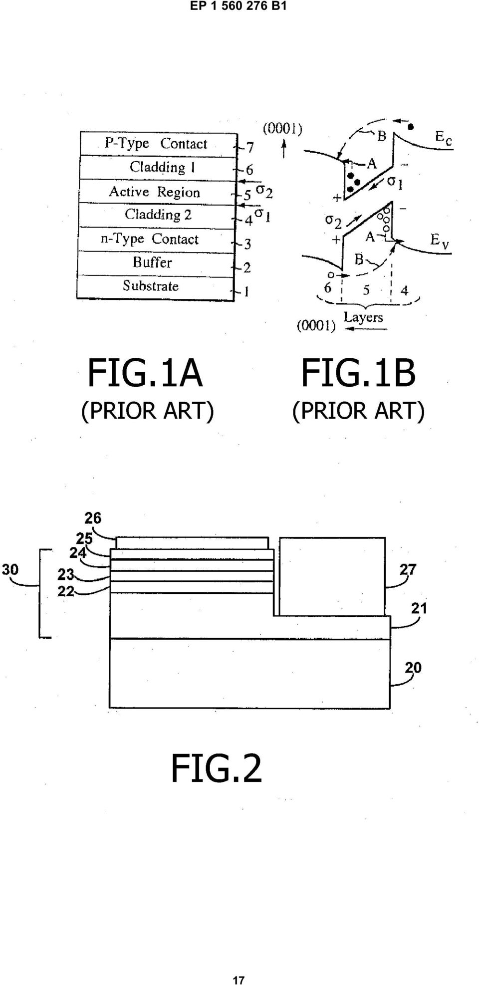
2 Description FIELD OF INVENTION [0001] The present invention relates to III-nitride light emitting devices. DESCRIPTION OF RELATED ART [0002] Semiconductor light-emitting devices including light emitting diodes (LEDs), resonant cavity light emitting diodes (RCLEDs), vertical cavity laser diodes (VCSELs), and edge emitting lasers are among the most efficient light sources currently available. Materials systems currently of interest in the manufacture of high-brightness light emitting devices capable of operation across the visible spectrum include Group III-V semiconductors, particularly binary, ternary, and quaternary alloys of gallium, aluminum, indium, and nitrogen, also referred to as III-nitride materials. Typically, III-nitride light emitting devices are fabricated by epitaxially growing a stack of semiconductor layers of different compositions and dopant concentrations on a sapphire, silicon carbide, III-nitride, or other suitable substrate by metal-organic chemical vapor deposition (MOCVD), molecular beam epitaxy (MBE), or other epitaxial techniques. The stack often includes one or more n-type layers doped with, for example, Si, formed over the substrate, a light emitting or active region formed over the n-type layer or layers, and one or more p-type layers doped with, for example, Mg, formed over the active region. III-nitride devices formed on conductive substrates may have the p- and n-contacts formed on opposite sides of the device. Often, III-nitride devices are fabricated on insulating substrates, such as sapphire, with both contacts on the same side of the device. Such devices are mounted so light is extracted either through the contacts (known as an epitaxyup device) or through a surface of the device opposite the contacts (known as a flip chip device). [0003] The crystal layers in III-nitride devices are often grown as strained wurtzite crystals on lattice-mismatched substrates such as sapphire. Such crystals exhibit two types of polarization, spontaneous polarization, which arises from the difference of alloy composition between layers of different composition, and piezoelectric polarization, which arises due to the strain in the layers of the device. The total polarization in a layer is the sum of the spontaneous and piezoelectric polarization. [0004] Fig. 1A is a sectional view schematically illustrating a typical conventional strained wurtzite nitride double heterostructure semiconductor, described in U.S. Patent 6,1,313. According to U.S. Patent 6,1,313, the illustrated substrate layer 1 may be any material suitable for growing nitride semiconductors, including spinel (MgAl 2 O 4 ), sapphire (Al 2 O 3 ), SiC (including 6H, 4H, and 3C), ZnS, ZnO, GaAs, AlN and GaN. The substrate thickness typically ranges from 0 mm to 1 mm. A buffer layer 2 on the substrate 1 can be formed of AlN, GaN, AlGaN, InGaN or the like. The buffer layer facilitates possible lattice mismatches between the substrate 1 and an overlying conductive contact layer 3. However, the buffer layer 2 may be omitted if the substrate has a lattice constant approximately equal to that of the nitride semiconductor. The buffer layer 2 may also be omitted with some nitride growth techniques. Depending upon the material composition, the buffer layer energy bandgap may range from 2.1 ev to 6.2 ev, with a thickness of about 0. mm to mm. [000] The n-type contact layer 3 is also typically formed from a nitride semiconductor, preferably GaN or InGaN with a thickness ranging from 0. mm to.0 mm, and a bandgap of approximately 3.4 ev for GaN and less for InGaN (depending upon the Indium concentration). A lower n-type or undoped cladding layer 4 on the conductive layer 3 conventionally comprises GaN or AlGaN, with a bandgap of 3.4 ev for GaN and greater for AlGaN (depending upon the Al concentration). Its thickness can range from 1 nm to 0 nm. [0006] Nitride double heterostructures typically employ InGaN as an active region over the lower cladding layer, with a thickness of 1 nm to 0 nm. The bandgap of this layer is typically 2.8 ev for blue emission, but may vary depending upon the Indium concentration. A top p-type or undoped cladding layer 6 over the active region is generally comprised of AlGaN or GaN, with a thickness and bandgap energy similar to that of the lower n-type cladding layer 4. A p-type GaN conductive contact layer 7 on the cladding layer 6 has an energy bandgap of about 3.4 ev and a thickness of about nm to 00 nm. A polarization-induced sheet charge occurs at the interface between layers due to different constituent materials. Of particular concern for the operation of a light emitter are the polarization-induced sheet charges adjacent to the active region. [0007] With the compound semiconductor illustrated in Fig. 1A, a negative polarization-induced sheet charge density σ1, with a magnitude such as 13 electrons/cm 2, is typically formed at the interface between the active region and the lower cladding layer 4. A positive sheet charge density σ2 of similar magnitude is formed at the interface between the active region and the upper cladding layer 6. The polarities of these charges depend upon the bonds of the crystal layers. In general, the density of a sheet charge will depend upon both a spontaneous factor arising from compositional differences between the two layers, and a piezoelectric strain arising from the lattice mismatch between the layers. For example, σ1 between an In 0.2 Ga 0.8 N active region and a GaN cladding layer 4 is about 8.3 x 12 electrons/cm 2. This is due to the % Indium content in the In 0.2 Ga 0.8 N active region (spontaneous polarization), and the strain in that layer arising from the lattice mismatch with the underlying GaN layer (piezoelectric polarization). 2

3 [0008] Fig. 1B illustrates the energy bands corresponding to the device structure of Fig. 1A. When the device is operating, the naturally occurring polarization field generated by σ1 and σ2 reduces the efficiency in a number of ways. First, the dipole leads to a spatial separation (movement in the opposite direction) of electrons and holes within the region. As illustrated, holes in the valence band E v are attracted to the negative sheet charge σ1 at one end of the active region, while electrons in the conduction band E c are attracted to the positive sheet charge σ2 at its other end. This spatial separation of free carriers lowers the probability of radiative recombination, reducing emission efficiency. Second, the energy barriers of the conduction and valence band quantum wells are reduced by quantization effects associated with the electric field. Thus, carriers below E v and above E c escape the well through the paths indicated by dashed lines A. Third, the presence of polarization-induced fields also leads to carrier overshoots, illustrated by carrier trajectories B, from the higher E c level on the σ1 side of the active region to the lower E c level on the σ2 side, and from the lower E v level on the σ2 side of the active region to the higher E v level on the σ1 side. SUMMARY 1 The invention is defined in claim 1. Embodiments of the invention are set out in the dependent claims. 2 [0009] In accordance with embodiments of the invention, a semiconductor light emitting device includes a light emitting layer sandwiched between two spacer layers. The difference between the net polarization in at least one of the spacer layers and the net polarization in the light emitting layer is less than in the device with conventional spacer layers, such as GaN spacer layers. The difference between the net polarization in at least one of the spacer layers and the net polarization in the light emitting layer is less than about 0.02 C/m 2. In some embodiments, at least one of the spacer layers is a quaternary alloy of aluminum, indium, gallium, and nitrogen. [00] Matching the net polarization in the spacer layers and the light emitting layers may move polarization-induced sheet charges away from the interfaces between the spacer layers and the light emitting layer to the interface between the p- and n-type regions and the spacer layers. Once the sheet-charges are spaced apart from the light emitting layer, in some embodiments the interface between the p- and n-type regions and the spacer layers is doped, which may reduce the polarization field across the light emitting layer. Accordingly, matching the net polarization in the spacer layers and the light emitting layers, and canceling sheet charges by doping may avoid the inefficiencies caused by polarization, described above. BRIEF DESCRIPTION OF THE DRAWINGS [0011] 3 4 Figs. 1A and 1B are a cross sectional view and an energy band diagram of a portion of a prior art light emitting device described in U.S. Patent 6,1,313. Fig. 2 is a cross sectional view of a device according to embodiments of the invention. Fig. 3 is an energy band diagram of a device where the spacer layers and active region have the same net polarization. Figs. 4 and are plots of aluminum composition vs. indium composition for quaternary III-nitride layers, including contour lines showing band gap energy and net polarization. Fig. 6 is an energy band diagram of a device where the spacer layers and active region have the same net polarization and where the sheet charges are eliminated with thick spacer layers and doping at the sheet charge interface. Figs. 7 and 8 are a plan view and a cross sectional view of a small junction light emitting device. Figs. 9 and are a plan view and a cross sectional view of a large junction light emitting device. Fig. 11 is an exploded view of a packaged light emitting device. DETAILED DESCRIPTION 0 [0012] Fig. 2 illustrates a device according to several embodiments of the invention. An n-type region 21 is formed over a suitable substrate, usually sapphire, SiC, or GaN. Active region 23 is sandwiched between two spacer layers, an n-type spacer layer 22 and a p-type spacer layer 24. Active region 23 may be a single light emitting layer or may include one or more quantum well layers separated by barrier layers. A p-type region 2 is formed over p-type spacer layer 24. P-contact 26 provides electrical contact to the p-side of the active region and n-contact 27 provides electrical contact to the n-side of the active region. Two possible arrangements of the p- and n-contacts are described below in Figs. 7-. [0013] In some embodiments of the invention, one or more of p-type spacer layer 24, n-type spacer layer 22, and the barrier layers separating the quantum wells in a multiple quantum well active region may be quaternary alloys of aluminum, indium, gallium, and nitrogen. The composition of aluminum, indium, and gallium in the barrier layers and/or in spacer 3

4 layers 22 and 24 are selected to match the net polarization within the light emitting layers of active region 23, or to minimize the difference in net polarization between the light emitting layers of the active region and the spacer layers and/or barrier layers. The net polarization in each layer is the sum of the spontaneous polarization and the piezoelectric polarization. The quaternary compositions required in the barrier layers and/or in spacer layers is based on the composition of the active region, which, along with the structure of the active region, determines the color of light emitted by the active region. Quaternary layers may be grown by techniques known in the art such as atmospheric pressure growth or pulsed metalorganic chemical vapor deposition (also known as pulsed atomic layer epitaxy). For a description of pulsed metalorganic chemical vapor deposition, see, for example, J. Zhang et al., "Pulsed Atomic Layer Epitaxy of Quaternary AlInGaN Layers," 79 Appl. Phys. Lett. 92 (01) and C. Chen et al., "Pulsed Metalorganic Chemical Vapor Deposition of Quaternary AlInGaN Layers and Multiple Quantum Wells for Ultraviolet Light Emission," 41 Jpn. J. Appl. Phys (02). [0014] The embodiments described below describe the characteristics of quaternary spacer layers. The same characteristics may be applied to form suitable quaternary barrier layers within a multiple quantum well active region. [001] In a first embodiment, the composition of the spacer layers are selected such that the difference in net polarization between the light emitting layers of the active region and at least one of the spacer layers is zero. The use of spacer layers with the same net polarization as the light emitting layers of the active region effectively cancels the sheet charges (shown in Fig. 1B) at the interface between the spacer layer and the active region. Fig. 3 illustrates a part of an energy band diagram for a device having a lightly doped or not intentionally doped active region and spacer layers, with quaternary spacer layers having the same net polarization as the active region (P 1 =P 2 ). Fig. 3 illustrates the canceling of sheet charges (e 1 =e 2 ) at the interfaces between the active region and the spacer layers on either side. Fig. 3 also illustrates that the sheet charges and resulting curves in the energy band diagram are not eliminated entirely, but are shifted from the interfaces between the active region and the spacer layers to the interfaces between the spacer layers and the p- and n-type regions. [0016] In a second embodiment, the composition of the spacer layers is selected such that the barrier height is enough to provide a sufficient barrier, but the difference in net polarization between the light emitting layers of the active region and the spacer layers is less than in a device with conventional spacer layers, such as GaN spacer layers. The barrier height is defined as the difference between the band gap in the spacer layer and the band gap in the light emitting layers of the active region. Generally, the higher the composition of aluminum and indium in a quaternary III-nitride layer, the more difficult it is to grow a layer of high crystal quality. As illustrated below, in most devices, spacer layers according to the first embodiment have high compositions of aluminum and indium. Though devices according to the second embodiment do not completely cancel the sheet charges at the interface between the spacer layer and the active region, these devices have potentially smaller sheet charges than devices with conventional barriers, and potentially better crystal quality spacer layers than devices according to the first embodiment. Both effects may increase the efficiency of devices according to the second embodiment. [0017] Fig. 4 illustrates how to determine the appropriate composition of the spacer layers for the first and second embodiments, given an active region composition. Fig. 4 is a contour plot of the polarization and the bandgap of an Al x In y Ga z N film vs. aluminum nitride composition and indium nitride composition. The Al x In y Ga z N film is assumed to be coherently grown on GaN. The solid contour lines represent the net polarization in C/m 2. The dashed contour lines represent the band gap in ev. Fig. 4 illustrates an example of an InGaN active layer of % indium, In 0.1 Ga 0.9 N (labeled "Active"), which may emit blue light when forward biased. In 0.1 Ga 0.9 N has a band gap of about 3.1 ev and a net polarization of about 0.01 C/m 2. In the example given in Fig. 4, the minimum barrier height is arbitrarily selected to be 0.2 ev. In other embodiments, the minimum barrier height may be larger or smaller, for example 0.3 ev or 0.1 ev. [0018] A composition range for spacer layers according to the first embodiment, where the spacer layers have the same net polarization as the active region, can be determined by following the 0.01 C/m 2 contour line in the direction of increasing indium composition and increasing aluminum composition until a composition with a band gap of at least 3.3 is reached, about Al 0. In 0.22 Ga 0.8 N. Any spacer layer composition at this point or above along the 0.01 C/m 2 contour line (the solid line marked "First" on Fig. 4) will provide a barrier height of at least 0.2 ev with the same net polarization as the active region. [0019] A composition range for spacer layers according to the second embodiment, where the spacer layers have a minimum barrier height and a net polarization less than that of a conventional spacer layer, is illustrated as shaded region "A" in Fig. 4. This region is bordered on the bottom right hand side by a curved line between about In 0.03 Ga 0.97 N and about Al 0. In 0.22 Ga 0.8 N, following a contour line representing the minimum barrier height of 0.2 ev. Region A is bordered on the top right hand side by a curved line between about Al 0. In 0.22 Ga 0.8 N and about Al 0.4 In 0.34 Ga 0.21 N, representing the first embodiment composition range. Region A is bordered on the left hand side by a curved line between about GaN and about Al 0.4 In 0.26 Ga 0.29 N, following a contour line representing the net polarization of a GaN spacer layer (labeled "GaN" on Fig. 4). Any spacer layer composition within this shaded region will have at least a 0.2 ev barrier and a net polarization less than that of a GaN spacer layer. The solid line within region A represents spacer layer compositions that have the same barrier height as a GaN spacer layer, but a net polarization less than that of a GaN 4

5 1 2 spacer layer. [00] Fig. illustrates an example of an InGaN active layer of % indium, In 0.2 Ga 0.8 N, which may emit green light when forward biased. The In 0.2 Ga 0.8 N active region (labeled "Active") has a net polarization of about C/m 2 and a band gap of about 2.9 ev. In the example given in Fig., the minimum barrier height is again arbitrarily selected to be 0.2 ev. [0021] A composition range for spacer layers according to the first embodiment, where the spacer layers have the same net polarization as the active region, is determined by following the C/m 2 contour line to the composition where the difference in band gap is at least 0.2eV, a composition of about Al 0.17 In 0.28 Ga 0. N, which has a band gap of 3.1 ev. Any composition at this point or above along the C/m 2 contour line (the line labeled "First" in Fig. ) will provide a sufficiently high barrier spacer layer with the same net polarization as the active region. [0022] A composition range for spacer layers according to the second embodiment, where the spacer layers have a minimum barrier height and a net polarization less than that of a conventional GaN spacer layer, is illustrated as shaded region "B" in Fig.. This region is bordered on the bottom right hand side by a curved line between about In 0.12 Ga 0.88 N and about Al 0.17 In 0.28 Ga 0. N, following a contour line representing the minimum barrier height of 0.2 ev. Region B is bordered on the top right hand side by a curved line between about Alo. 17 In 0.28 Ga 0. N and about Al 0.4 In 0. Ga 0.1 N, representing the first embodiment composition range. Region B is bordered on the left hand side by a curved line between about GaN and about Al 0.4 In 0.26 Ga 0.29 N, following a contour line representing the net polarization of a GaN spacer layer (labeled "GaN"). Any spacer layer composition within this shaded region will have a least a 0.2 ev barrier and a net polarization less than a GaN spacer layer. The solid line within region B represents spacer layer compositions with the same barrier height as a GaN spacer layer, but a net polarization less than that of a GaN spacer layer. [0023] Though Figs. 4 and end at aluminum nitride and indium nitride compositions of 4%, layers with greater aluminum nitride and indium nitride compositions may be appropriate. The data illustrated in Figs. 4 and is not meant to limit the invention. The data in Figs. 4 and were calculated using techniques well known in the art and using the following material parameters. The data illustrated in Figs. 4 and may change if different values are used for the following material parameters: AlN GaN InN a-lattice a 0 (Å) c-lattice c 0 (Å) Band gap E g (ev) Elastic constants c13 (GPa) c33 (GPa) Spontaneous polarization P sp (C/m 2 ) Piezoelectric constants e31 (C/m 2 ) e33 (C/m 2 ) AlGaN InGaN AlInN Bowing parameter B(eV) [0024] The data in Figs. 4 and were calculated as follows. Given the a-lattice constants a k and elastic constants c ij,k of AlN, GaN, and InN, the a-lattice constant a AlInGaN and strain ε zz in a quaternary layer grown on GaN may be calculated according to the following equations: 0
![[0021] A composition range for spacer layers according to the first embodiment, where the spacer layers have the same net polarization as the active region, is determined by following the 0.](/docs-images/57/5693049/images/page_5.jpg "021 C/m 2 contour line to the composition where the difference in band gap is at least 0.2eV, a composition of about Al 0.17 In 0.28 Ga 0. N, which has a band gap of 3.1 ev.")
6 [002] Given the band gap E i of AlN, GaN, and InN and bowing parameters of b ij of each ternary alloy, the band gap of a free standing quaternary layer may be calculated according to the following equations: 1 2 [0026] The band gap of a strained quaternary layer grown on GaN (as illustrated by dashed contour lines in Figs. 4 and ) is related to the strain of the layer ε zz (calculated above) and the band gap of the free standing material, according to the equations: 3 [0027] Given the spontaneous polarization P sp,k and piezoelectric constants e ij,k for AlN, GaN, and InN, the spontaneous polarization P sp and piezoelectric polarization P pz in a quaternary layer grown on GaN may be calculated according to the following equations: 4 The net polarization in the quaternary layer grown on GaN is then given by: 0 [0028] As illustrated in Fig. 3, matching the net polarization of the spacer layers and the active region cancels the sheet charges at the interfaces between the spacer layers and the active region. These sheet charges are shifted to the interface between the p- and n-type regions and the spacer layers, where differences in composition between the layers that form the interface result in different net polarization on either side of the interface. Shifting the sheet charges away from the active region does not totally eliminate their effect on the active regions. The "tilt" of the energy bands in the active region illustrated in Fig. 3 is caused by the sheet charges at the interfaces between the spacer layers and the p- and n-type regions. 6
![4 and ) is related to the strain of the layer ε zz (calculated above) and the band gap of the free standing material, according to the equations: 3 [0027] Given the spontaneous polarization P sp,k](/docs-images/57/5693049/images/page_6.jpg "and piezoelectric constants e ij,k for AlN, GaN, and InN, the spontaneous polarization P sp and piezoelectric polarization P pz in a quaternary layer grown on GaN may be calculated according to the")
7 [0029] To eliminate sheet charges, U.S. Patent 6,1,313 teaches "incorporating various dopants into the semiconductor. The dopant impurity should be of a type that does not diffuse away from its intended position. The dopants ionize, based upon their energy levels, into either positive or negative charge states, which are opposite to the interfacial polarization-induced charge states, to cancel or reduce its effect." U.S. Patent 6,1,313 incorporates the dopants at the interfaces between the spacer layers and the active region. The incorporation of dopants, especially Mg, so close to the active region can degrade the crystal quality of the active region. [00] In some embodiments of the invention, the sheet charges are eliminated by making the spacer layers sufficiently thick to "screen" the active region from the sheet charges at the interfaces between the p- and n-type regions and the spacer layers, then doping the interfaces with the sheet charge with a dopant that neutralizes the sheet charge. In embodiments without thick spacer layers, the spacer layers often have a thickness between about 0 angstroms and about 0 angstroms. In embodiments with thick spacer layers, the spacer layers may have a thickness between about 00 angstroms and the critical thickness of the spacer layer, defined as the maximum thickness of the spacer layer that can be grown without cracking or relaxing. The thick spacer layers usually have a thickness between about 0 angstroms and about 00 angstroms. In general, the thickness of the thick spacer layers is chosen to be thick enough to shield the active region from the doping to cancel the sheet charges, and thin enough to permit growth of a high crystal quality spacer layer. [0031] A negative sheet charge accumulates at the interface between n-type or undoped spacer layer 22 and n-type region 21. This sheet charge may be canceled by incorporating a region of highly n-type doped material as close to the interface as possible. The highly doped region may be in the part of n-type region 21 or spacer layer 22 adjacent to the interface. For example, a region angstroms thick and having a Si concentration between about 1x 18 cm -3 and 1x cm -3 may be incorporated in n-type region 21 or spacer layer 22, immediately adjacent to the interface between these two layers. More preferably, the highly doped region has a Si concentration between about x 19 cm -3 and 1x cm -3. Similarly, a positive sheet charge accumulates at the interface between p-type spacer layer 24 and p-type region 2. This sheet charge may be canceled by incorporating a region of highly p-type doped material in the part of p-type region 2 or spacer layer 24 adjacent to the interface. For example, a region angstroms thick and having a Mg concentration between about 1x 18 cm -3 and 1x cm -3 may be incorporated in p-type region 2 or spacer layer 24, immediately adjacent to the interface between these two layers. More preferably, the highly doped region has a Mg concentration between about x 19 cm -3 and 1x cm -3. [0032] The amount of doping required at the interfaces between the spacer layers and the p- and n-type regions may depend on the magnitude of the sheet charge, which depends on the compositions of the layers in the device. Generally, the thickness and dopant concentration are selected such that the dopant concentration in the highly doped area times the thickness of the highly doped area is about equal to the sheet charge at the interface. Accordingly, the higher the dopant concentration in the highly doped area, the thinner this area needs to be to cancel the sheet charge. In some embodiments, the sheet charges may be canceled by incorporating lower concentrations of dopants in the n- and p- type regions or in the spacer layers over greater thicknesses. In addition, as the composition of indium in the active region increases, the magnitude of the sheet change increases. In the examples given above, the sheet charges in the device with % indium quantum wells may be twice the magnitude of the sheet charges in the device with % indium quantum wells. [0033] Fig. 6 is an energy band diagram with a device where the spacer layers and active region have the same net polarization and where the sheet charges are eliminated with thick spacer layers and doping at the sheet charge interface. As illustrated in Fig. 6, both the bending of the energy bands at the interfaces between the layers and the tilt of the energy bands in the active region is eliminated. [0034] Fig. 7 is a plan view of a small junction device (i.e. an area less than one square millimeter). Fig. 8 is a cross section of the device shown in Fig. 7, taken along axis CC. Figs. 7 and 8 illustrate an arrangement of contacts that may be used with any of the epitaxial structures illustrated in Fig. 2 and described above. The device shown in Figs. 7 and 8 has a single via 31 etched down to an n-type layer of epitaxial structure below the active region. An n-contact 27 is deposited in via 31. N-via 31 is located at the center of the device to provide uniformity of current and light emission. A p-contact 26 provides electrical contact to the p-side of the active region of epitaxial structure. N-contact 27 is separated from the p-contact 26 by one or more dielectric layers 32. A p-submount connection 34, for example, a wettable metal for connecting to solder, connects to p-contact 26 and an n-submount connection 33 connects to n-contact 27. [003] As illustrated in Fig. 7, the device is connected to a submount by three submount connections, two p-submount connections 34 and one n-submount connection 33. N-submount connection 33 may be located anywhere within n- contact region 27 (surrounded by insulating layer 32) and need not be located directly over via 31. Similarly, p-submount connections 34 may be located anywhere on p-contact 26. As a result, the connection of the device to a submount is not limited by the shape or placement of p-contact 26 and n-contact 27. [0036] Fig. 9 is a plan view of a large junction device (i.e. an area greater than or equal to one square millimeter). Fig. is a cross section of the device shown in Fig. 9, taken along axis DD. Figs. 9 and also illustrate an arrangement of contacts that may be used with any of the epitaxial structures illustrated in Fig. 2 and described above. The active 7

8 1 region of epitaxial structure is separated into four regions separated by three trenches in which n-contacts 27 are formed. Each region is connected to a submount by four p-submount connections 34 formed on p-contact 26. N-contact 27 surrounds the four active regions. N-contact 27 is connected to a submount by six n-submount connections 33. The n- and p-contacts may be electrically isolated by an insulating layer 32. [0037] Fig. 11 is an exploded view of a packaged light emitting device. A heat-sinking slug 0 is placed into an insertmolded leadframe. The insert-molded leadframe is, for example, a filled plastic material molded around a metal frame 6 that provides an electrical path. Slug 0 may include an optional reflector cup 2. The light emitting device die 4, which may be any of the devices described above, is mounted directly or indirectly via a thermally conducting submount 3 to slug 0. An optical lens 8 may be added. [0038] Reducing the effect of polarization fields on the active region according to embodiments of the invention may have several advantages. First, carrier recombination rate may increase, increasing the quantum efficiency of the device. Second, the carrier recombination lifetime may be reduced, reducing the carrier density at a given current density, and resulting in improved quantum efficiency at increased drive currents. Third, electron and hole injection efficiency may increase, leading to more uniform filling of the active region with carriers. Each of these effects may improve the efficiency of the device. Claims 1. A III-nitride semiconductor light emitting device comprising: 2 first (22) and second (24) spacer layers; a light emitting layer (23) sandwiched between the first (22) and second (24) spacer layers; an n-type region (21) adjacent to a surface of the first spacer layer (22) opposite the light emitting layer; a p-type region (2) adjacent to a surface of the second spacer layer (24) opposite the light emitting layer, wherein a difference between a net polarization in at least one of the spacer layers (22, 24) and a net polarization in the light emitting layer (23) is less than a difference between a net polarization in GaN and the net polarization in the light emitting layer (23), and a difference between the net polarization in at least one of the spacer layers (22, 24) and the net polarization in the light emitting layer (23) is less than 0.02 C/m 2 ; characterized in that said light emitting device further comprises: 3 a highly doped region of n-type material adjacent to an interface between the first spacer layer (22) and the n-type region (21), a thickness and dopant concentration of the highly doped region of n-type material being selected such that the dopant concentration in the highly doped region times the thickness of the highly doped region is about equal to the sheet charge at the interface between the first spacer layer (22) and the n-type region (21); and/or a highly doped region of p-type material adjacent to an interface between the second spacer layer (24) and the p-type region (2), a thickness and dopant concentration of the highly doped region of p-type material being selected such that the dopant concentration in the highly doped region times the thickness of the highly doped region is about equal to the sheet charge at the interface between the second spacer layer (24) and the p-type region (2) The device of claim 1 wherein at least one of the spacer layers (22, 24) comprises Al x In y Ga z N, where 0<x 1, 0<y 1, and 0<z The device of claim 1 wherein the light emitting layer (23) comprises at least one layer of InGaN The device of claim 1 wherein the difference between the net polarization in at least one of the spacer layers (22, 24) and the net polarization in the light emitting layer (23) is less than 0.01 C/m 2.. The device of claim 1 wherein the difference between the net polarization in at least one of the spacer layers (22, 24) and the net polarization in the light emitting layer (23) is less than 0.00 C/m The device of claim 1 wherein the difference between the net polarization in at least one of the spacer layers (22, 24) and the net polarization in the light emitting layer (23) is 0 C/m The device of claim 1 wherein a difference between a band gap in at least one of the spacer layers (22, 24) and a band gap in the light emitting layer (23) is greater than 0.1 ev. 8
![N-contact 27 is connected to a submount by six n-submount connections 33. The n- and p-contacts may be electrically isolated by an insulating layer 32. [0037] Fig.](/docs-images/57/5693049/images/page_8.jpg "11 is an exploded view of a packaged light emitting device. A heat-sinking slug 0 is placed into an insertmolded leadframe.")
9 8. The device of claim 1 wherein a difference between a band gap in at least one of the spacer layers (22, 24) and a band gap in the light emitting layer (23) is greater than 0.2 ev. 9. The device of claim 1 wherein the light emitting layer (23) comprises at least one InGaN layer with a composition between In 0.0 Ga 0.9 N and In 0.1 Ga 0.8 N.. The device of claim 9 wherein: at least one of the spacer layers (22, 24) is a quaternary alloy of aluminum, indium, gallium, and nitrogen; and an aluminum composition in the quaternary alloy spacer layer is greater than or equal to %. 11. The device of claim wherein the indium composition in the quaternary alloy spacer layer is greater than or equal to 22% The device of claim 9 wherein at least one of the spacer layers (22, 24) is a quaternary alloy of aluminum, indium, gallium, and nitrogen. 13. The device of claim 9 wherein at least one of the spacer layers (22, 24) is a quaternary alloy of aluminum, indium, gallium, and nitrogen; and an aluminum composition in the quaternary alloy spacer layer is greater than zero and less than or equal to %; and an indium composition in the quaternary alloy spacer layer is greater than zero and less than or equal to 22% The device of claim 1 wherein the light emitting layer (23) comprises at least one InGaN layer with a composition between In 0.1 Ga 0.8 N and In 0. Ga 0. N. 1. The device of claim 14 wherein: at least one of the spacer layers (22, 24) is a quaternary alloy of aluminum, indium, gallium, and nitrogen; and an aluminum composition in the quaternary alloy spacer layer is greater than or equal to 17%. 16. The device of claim 1 wherein the indium composition in the quaternary alloy spacer layer is greater than or equal to 28% The device of claim 14 wherein at least one of the spacer layers (22, 24) is a quaternary alloy of aluminum, indium, gallium, and nitrogen. 18. The device of claim 14 wherein at least one of the spacer layers (22, 24) is a quaternary alloy of aluminum, indium, gallium, and nitrogen; and an aluminum composition in the quaternary alloy spacer layer is greater than zero and less than or equal to 17%; and an indium composition in the quaternary alloy spacer layer is greater than zero and less than or equal to 28%. 19. The device of claim 1 wherein at least one of the spacer layers (22, 24) has a thickness between about 0 angstroms and about 00 angstroms. 4. The device of claim 1 wherein at least one of the spacer layers (22, 24) has a thickness between about 0 angstroms and a critical thickness of the spacer layer The device of claim 1 wherein the highly doped region of n-type material has a dopant concentration between about 1x 18 cm -3 and about 1x cm -3 and a thickness between about angstroms and about 0 angstroms. 22. The device of claim 21 wherein the highly doped region of n-type material has a dopant concentration between about x 19 cm -3 and about 1x cm The device of claim 21 wherein the highly doped region of n-type material is located within the first spacer layer (22). 24. The device of claim 21 wherein the highly doped region of n-type material is located within the n-type region (21). 2. The device of claim 1 wherein the highly doped region of p-type material has a dopant concentration between about 9

10 1x 18 cm -3 and about 1x cm -3 and a thickness between about angstroms and about 0 angstroms. 26. The device of claim 2 wherein the highly doped region of p-type material has a dopant concentration between about x 19 cm -3 and about 1x cm The device of claim 2 wherein the highly doped region of p-type material is located within the second spacer layer (24). 28. The device of claim 2 wherein the highly doped region of p-type material is located within the p-type region (2). 29. The device of claim 1 wherein the light emitting layer (23) is a first quantum well, the device further comprising a second quantum well, and a barrier layer disposed between the first quantum well and the second quantum well. 1. The device of claim 29 wherein the barrier layer comprises Al x In y Ga z N, where 0<x 1, 0<y 1, and 0<z The device of claim 29 wherein a net polarization in the barrier layer is less than a net polarization in GaN, and a difference between the net polarization in the barrier layer and a net polarization in at least one of the quantum wells is less than 0.02 C/m The device of claim 29 wherein the difference between the net polarization in the barrier layer and the net polarization in at least one of the quantum wells is less than 0.01 C/m The device of claim 29 wherein the difference between the net polarization in the barrier layer and the net polarization in at least one of the quantum wells is less than 0.00 C/m The device of claim 29 wherein the difference between the net polarization in the barrier layer and the net polarization in at least one of the quantum wells is 0 C/m The device of claim 1 wherein the light emitting layer (23) comprises Al x In y Ga z N, where 0<x 1, 0<y 1, and 0<z The device of claim 1 wherein the light emitting layer (23) comprises: 3 an active region comprising a first quantum well, a second quantum well, and a barrier layer disposed between the first quantum well and the second quantum well 37. The device of claim 36 wherein the barrier layer comprises Al x In y Ga z N, where 0<x 1, 0<y 1, and 0<z The device of claim 36 wherein the difference between the net polarization in the barrier layer and the net polarization in at least one of the quantum wells is less than 0.01 C/m The device of claim 36 wherein the difference between the net polarization in the barrier layer and the net polarization in at least one of the quantum wells is less than 0.00 C/m The device of claim 36 wherein the difference between the net polarization in the barrier layer and the net polarization in at least one of the quantum wells is 0 C/m 2. Patentansprüche 0 1. Licht emittierende III-Nitrid-Halbleiteranordnung, umfassend: eine erste (22) und zweite (24) Abstandsschicht; eine Licht emittierende Schicht (23), die zwischen der ersten (22) und zweiten (24) Abstandsschicht angeordnet ist; einen n-typ-bereich (21) in Angrenzung an eine Oberfläche der ersten Abstandsschicht (22); einen p-typ-bereich (2) in Angrenzung an eine Oberfläche der zweiten Abstandsschicht (24) gegenüber der Licht emittierenden Schicht, wobei eine Differenz zwischen einer Nettopolarisation in mindestens einer der Abstandsschichten (22, 24) und
. 29.")
11 1 einer Nettopolarisation in der Licht emittierenden Schicht (23) geringer als eine Differenz zwischen einer Nettopolarisation in GaN und der Nettopolarisation in der Licht emittierenden Schicht (23) ist, und eine Differenz zwischen der Nettopolarisation in mindestens einer der Abstandsschichten (22, 24) und der Nettopolarisation in der Licht emittierenden Schicht (23) geringer als 0,02 C/m 2 ist; dadurch gekennzeichnet, dass die Licht emittierende Anordnung weiterhin einen hoch dotierten Bereich aus n-typ-material in Angrenzung an eine Schnittstelle zwischen der ersten Abstandsschicht (22) und dem n-typ-bereich (21) umfasst, wobei eine Dicke und Dotierungskonzentration des hoch dotierten Bereichs aus n-typ-material so ausgewählt wird, dass die Dotierungskonzentration in dem hoch dotierten Bereich mal der Dicke des hoch dotierten Bereichs in etwa der Schichtladung an der Schnittstelle zwischen der ersten Abstandsschicht (22) und dem n-typ-bereich (21) entspricht; und/oder einen hoch dotierten Bereich aus p-typ-material in Angrenzung an eine Schnittstelle zwischen der zweiten Abstandsschicht (24) und dem p-typ-bereich (2), wobei eine Dicke und Dotierungskonzentration des hoch dotierten Bereichs aus p-typ-material so ausgewählt wird, dass die Dotierungskonzentration in dem hoch dotierten Bereich mal der Dicke des hoch dotierten Bereichs in etwa der Schichtladung an der Schnittstelle zwischen der zweiten Abstandsschicht (24) und dem p-typ-bereich (2) entspricht. 2. Anordnung nach Anspruch 1, wobei mindestens eine der Abstandsschichten (22, 24) Al x In y Ga z N umfasst, wobei 0 < x 1, 0 < y 1 und 0 < z Anordnung nach Anspruch 1, wobei die Licht emittierende Schicht (23) mindestens eine Schicht aus InGaN umfasst. 4. Anordnung nach Anspruch 1, wobei die Differenz zwischen der Nettopolarisation in mindestens einer der Abstandsschichten (22, 24) und der Nettopolarisation in der Licht emittierenden Schicht (23) geringer als 0,01 C/m 2 ist. 2. Anordnung nach Anspruch 1, wobei die Differenz zwischen der Nettopolarisation in mindestens einer der Abstandsschichten (22, 24) und der Nettopolarisation in der Licht emittierenden Schicht (23) geringer als 0,00 C/m 2 ist. 6. Anordnung nach Anspruch 1, wobei die Differenz zwischen der Nettopolarisation in mindestens einer der Abstandsschichten (22, 24) und der Nettopolarisation in der Licht emittierenden Schicht (23) 0 C/m 2 beträgt. 7. Anordnung nach Anspruch 1, wobei eine Differenz zwischen einem Bandabstand in mindestens einer der Abstandsschichten (22, 24) und einem Bandabstand in der Licht emittierenden Schicht (23) größer als 0,1 ev ist Anordnung nach Anspruch 1, wobei eine Differenz zwischen einem Bandabstand in mindestens einer der Abstandsschichten (22, 24) und einem Bandabstand in der Licht emittierenden Schicht (23) größer als 0,2 ev ist. 9. Anordnung nach Anspruch 1, wobei die Licht emittierende Schicht (23) mindestens eine InGaN-Schicht mit einer Zusammensetzung zwischen In 0,0 Ga 0,9 N und In 0,1 Ga 0,8 N umfasst.. Anordnung nach Anspruch 9, wobei: 4 mindestens eine der Abstandsschichten (22, 24) eine quaternäre Legierung aus Aluminium, Indium, Gallium und Stickstoff ist; und eine Aluminiumzusammensetzung in der Abstandsschicht aus der quaternären Legierung größer als oder gleich % ist. 11. Anordnung nach Anspruch, wobei die Indiumzusammensetzung in der Abstandsschicht aus quaternärer Legierung größer als oder gleich 22% ist Anordnung nach Anspruch 9, wobei mindestens eine der Abstandsschichten (22, 24) eine quaternäre Legierung aus Aluminium, Indium, Gallium und Stickstoff ist. 13. Anordnung nach Anspruch 9, wobei mindestens eine der Abstandsschichten (22, 24) eine quaternäre Legierung aus Aluminium, Indium, Gallium und Stickstoff ist; und eine Aluminiumzusammensetzung in der Abstandsschicht aus quaternärer Legierung größer als Null und geringer als oder gleich % ist; und eine Indiumzusammensetzung in der Abstandsschicht aus quaternärer Legierung größer als Null und geringer als oder gleich 22% ist. 11
 und dem n-typ-bereich (21) umfasst, wobei eine Dicke und Dotierungskonzentration des hoch dotierten Bereichs aus n-typ-material so ausgewählt wird, dass die Dotierungskonzentration in dem hoch")
12 14. Anordnung nach Anspruch 1, wobei die Licht emittierende Schicht (23) mindestens eine InGaN-Schicht mit einer Zusammensetzung zwischen In 0,1 Ga 0,8 N und In 0, Ga 0, N umfasst. 1. Anordnung nach Anspruch 14, wobei: mindestens eine der Abstandsschichten (22, 24) eine quaternäre Legierung aus Aluminium, Indium, Gallium und Stickstoff ist; und eine Aluminiumzusammensetzung in der Abstandsschicht aus quaternärer Legierung größer als oder gleich 17% ist. 16. Anordnung nach Anspruch 1, wobei die Indiumzusammensetzung in der Abstandsschicht aus quaternärer Legierung größer als oder gleich 28% ist Anordnung nach Anspruch 14, wobei mindestens eine der Abstandsschichten (22, 24) eine quaternäre Legierung aus Aluminium, Indium, Gallium und Stickstoff ist. 18. Anordnung nach Anspruch 14, wobei mindestens eine der Abstandschichten (22, 24) eine quaternäre Legierung aus Aluminium, Indium, Gallium und Stickstoff ist; und eine Aluminiumzusammensetzung in der Abstandsschicht aus quaternärer Legierung größer als Null und geringer als oder gleich 17% ist; und eine Indiumzusammensetzung in der Abstandschicht aus quaternärer Legierung größer als Null und geringer als oder gleich 28% ist Anordnung nach Anspruch 1, wobei mindestens eine der Abstandsschichten (22, 24) eine Dicke zwischen etwa 0 Angström und etwa 00 Angström aufweist.. Anordnung nach Anspruch 1, wobei mindestens eine der Abstandsschichten (22, 24) eine Dicke zwischen etwa 0 Angström und einer kritischen Dicke der Abstandsschicht aufweist. 21. Anordnung nach Anspruch 1, wobei der hochdotierte Bereich aus n-typ-material eine Dotierungskonzentration zwischen etwa 1x 18 cm -3 und etwa 1x cm -3 und eine Dicke zwischen etwa Angström und etwa 0 Angström aufweist Anordnung nach Anspruch 21, wobei der hochdotierte Bereich aus n-typ-material eine Dotierungskonzentration zwischen etwa x 19 cm -3 und etwa 1x cm -3 aufweist. 23. Anordnung nach Anspruch 21, wobei der hochdotierte Bereich aus n-typ-material innerhalb der ersten Abstandsschicht (22) angeordnet ist. 24. Anordnung nach Anspruch 21, wobei der hochdotierte Bereich aus n-typ-material innerhalb des n-typ-bereichs angeordnet (21) ist Anordnung nach Anspruch 1, wobei der hochdotierte Bereich aus p-typ-material eine Dotierungskonzentration zwischen etwa 1x 18 cm -3 und etwa 1x cm -3 und eine Dicke zwischen etwa Angström und etwa 0 Angström aufweist. 26. Anordnung nach Anspruch 2, wobei der hochdotierte Bereich aus p-typ-material eine Dotierungskonzentration zwischen etwa x 19 cm -3 und etwa 1x cm -3 aufweist Anordnung nach Anspruch 2, wobei der hochdotierte Bereich aus p-typ-material innerhalb der zweiten Abstandsschicht (24) angeordnet ist. 28. Anordnung nach Anspruch 2, wobei der hochdotierte Bereich aus p-typ-material innerhalb des p-typ-bereichs (2) angeordnet ist. 29. Anordnung nach Anspruch 1, wobei die Licht emittierende Schicht (23) eine erste Quantum-Well ist, wobei die Anordnung weiterhin eine zweite Quantum-Well umfasst und eine Barriereschicht zwischen der ersten Quantum- Well und der zweiten Quantum-Well angeordnet ist. 12

13 . Anordnung nach Anspruch 29, wobei die Barriereschicht Al x In y Ga z N umfasst, wobei 0 < x 1, 0 < y 1 und 0 < z Anordnung nach Anspruch 29, wobei eine Nettopolarisation in der Barriereschicht geringer als eine Nettopolarisation in GaN ist und eine Differenz zwischen der Nettopolarisation in der Barriereschicht und einer Nettopolarisation in mindestens einer der Quantum-Wells geringer als 0,02 C/m 2 ist. 32. Anordnung nach Anspruch 29, wobei die Differenz zwischen der Nettopolarisation in der Barriereschicht und der Nettopolarisation in mindestens einer der Quantum-Wells geringer als 0,01 C/m 2 ist. 33. Anordnung nach Anspruch 29, wobei die Differenz zwischen der Nettopolarisation in der Barriereschicht und der Nettopolarisation in mindestens einer der Quantum-Wells geringer als 0,00 C/m 2 ist Anordnung nach Anspruch 29, wobei die Differenz zwischen der Nettopolarisation in der Barriereschicht und der Nettopolarisation in mindestens einer der Quantum-Wells 0 C/m 2 beträgt. 3. Anordnung nach Anspruch 1, wobei die Licht emittierende Schicht (23) Al x In y Ga z N umfasst, wobei 0 < x 1, 0 < y 1 und 0 < z Anordnung nach Anspruch 1, wobei die Licht emittierende Schicht (23) umfasst: einen aktiven Bereich mit einer ersten Quantum-Well, einer zweiten Quantum-Well sowie einer zwischen der ersten Quantum-Well und der zweiten Quantum-Well angeordneten Barriereschicht Anordnung nach Anspruch 36, wobei die Barriereschicht Al x In y Ga z N umfasst, wobei 0 < x 1, 0 < y 1 und 0 < z Anordnung nach Anspruch 36, wobei die Differenz zwischen der Nettopolarisation in der Barriereschicht und der Nettopolarisation in mindestens einer der Quantum-Wells geringer als 0,01 C/m 2 ist. 39. Anordnung nach Anspruch 36, wobei die Differenz zwischen der Nettopolarisation in der Barriereschicht und der Nettopolarisation in mindestens einer der Quantum-Wells geringer als 0,00 C/m 2 ist.. Anordnung nach Anspruch 36, wobei die Differenz zwischen der Nettopolarisation in der Barriereschicht und der Nettopolarisation in mindestens einer der Quantum-Wells 0 C/m 2 beträgt. 3 Revendications 1. Dispositif électroluminescent à semi-conducteur de nitrure III, comprenant : 4 0 une première (22) et une seconde (24) couche d espacement ; une couche électroluminescente (23) prise en sandwich entre la première (22) et le seconde (24) couche d espacement ; une région de type n (21) adjacente à une surface de la première couche d espacement (22) opposée à la couche électroluminescente ; une région de type p (2) adjacente à une surface de la seconde couche d espacement (24) opposée à la couche électroluminescente, dans lequel la différence entre une polarisation nette dans au moins l une des couches d espacement (22, 24) et une polarisation nette dans la couche électroluminescente (23) est inférieure à la différence entre une polarisation nette dans le GaN et la polarisation nette dans la couche électroluminescente (23) et la différence entre la polarisation nette dans au moins l une des couches d espacement (22, 24) et la polarisation nette dans la couche électroluminescente (23) est inférieure à 0,02 C/m 2 ; caractérisé en ce que ledit dispositif électroluminescent comprend en outre : une région fortement dopée d un matériau de type n adjacente à une interface entre la première couche d espacement (22) et la région de type n (21), l épaisseur et la concentration de dopant de la région fortement dopée du matériau de type n étant choisies de sorte que le produit de la concentration de dopant dans la région fortement dopée fois l épaisseur de la région fortement dopée soit à peu près égal à la charge par feuille à l interface entre la première couche d espacement (22) et la région de type n (21) ; et/ou 13

14 une région fortement dopée d un matériau de type p adjacente à une interface entre la seconde couche d espacement (24) et la région de type p (2), l épaisseur et la concentration de dopant de la région fortement dopée du matériau de type p étant choisies de sorte que le produit de la concentration de dopant dans la région fortement dopée fois l épaisseur de la région fortement dopée soit à peu près égal à la charge par feuille à l interface entre la seconde couche d espacement (24) et la région de type p (2). 2. Dispositif selon la revendication 1, dans lequel au moins l une des couches d espacement (22, 24) comprend du Al x In y Ga z N, où 0 < x 1, 0 < y 1 et 0 < z Dispositif selon la revendication 1, dans lequel la couche électroluminescente (23) comprend au moins une couche d InGaN Dispositif selon la revendication 1, dans lequel la différence entre la polarisation nette dans au moins l une des couches d espacement (22, 24) et la polarisation nette dans la couche électroluminescente (23) est inférieure à 0,01 C/m 2.. Dispositif selon la revendication 1, dans lequel la différence entre la polarisation nette dans au moins l une des couches d espacement (22, 24) et la polarisation nette dans la couche électroluminescente (23) est inférieure à 0,00 C/m Dispositif selon la revendication 1, dans lequel la différence entre la polarisation nette dans au moins l une des couches d espacement (22, 24) et la polarisation nette dans la couche électroluminescente (23) est de 0 C/m Dispositif selon la revendication 1, dans lequel la différence entre un intervalle entre bandes dans au moins l une des couches d espacement (22, 24) et un intervalle entre bandes dans la couche électroluminescente (23) est supérieure à 0,1 ev. 8. Dispositif selon la revendication 1, dans lequel la différence entre un intervalle entre bandes dans au moins l une des couches d espacement (22, 24) et un intervalle entre bandes dans la couche électroluminescente (23) est supérieure à 0,2 ev. 9. Dispositif selon la revendication 1, dans lequel la couche électroluminescente (23) comprend au moins une couche d InGaN avec une composition comprise entre In 0,0 Ga 0,9 N et In 0,1 Ga 0,8 N. 3. Dispositif selon la revendication 9, dans lequel : au moins l une des couches d espacement (22, 24) est un alliage quaternaire d aluminium, d indium, de gallium et d azote ; et une composition d aluminium dans la couche d espacement d alliage quaternaire est supérieure ou égale à %. 11. Dispositif selon la revendication, dans lequel la composition d indium dans la couche d espacement d alliage quaternaire est supérieure ou égale à 22 % Dispositif selon la revendication 9, dans lequel au moins l une des couches d espacement (22, 24) est un alliage quaternaire d aluminium, d indium, de gallium et d azote Dispositif selon la revendication 9, dans lequel au moins l une des couches d espacement (22, 24) est un alliage quaternaire d aluminium, d indium, de gallium et d azote ; et une composition d aluminium dans la couche d espacement d alliage quaternaire est supérieure à zéro et inférieure ou égale à % ; et une composition d indium dans la couche d espacement d alliage quaternaire est supérieure à zéro et inférieure ou égale à 22 %. 14. Dispositif selon la revendication 1, dans lequel la couche électroluminescente (23) comprend au moins une couche d InGaN avec une composition comprise entre In 0,1 Ga 0,8 N et In 0, Ga 0, N. 1. Dispositif selon la revendication 14, dans lequel : 14
 comprend du Al x In y Ga z N, où 0 < x 1, 0 < y 1 et 0 < z 1. 3.")
15 au moins l une des couches d espacement (22, 24) est un alliage quaternaire d aluminium, d indium, de gallium et d azote ; et une composition d aluminium dans la couche d espacement d alliage quaternaire est supérieure ou égale à 17 %. 16. Dispositif selon la revendication 1, dans lequel la composition d indium dans la couche d espacement d alliage quaternaire est supérieure ou égale à 28 % Dispositif selon la revendication 14, dans lequel au moins l une des couches d espacement (22, 24) est un alliage quaternaire d aluminium, d indium, de gallium et d azote. 18. Dispositif selon la revendication 14, dans lequel au moins l une des couches d espacement (22, 24) est un alliage quaternaire d aluminium, d indium, de gallium et d azote ; et une composition d aluminium dans la couche d espacement d alliage quaternaire est supérieure à zéro et inférieure ou égale à 17 % ; et une composition d indium dans la couche d espacement d alliage quaternaire est supérieure à zéro et inférieure ou égale à 28 %. 19. Dispositif selon la revendication 1, dans lequel au moins l une des couches d espacement (22, 24) a une épaisseur comprise entre environ 0 angströms et environ 00 angströms.. Dispositif selon la revendication 1, dans lequel au moins l une des couches d espacement (22, 24) a une épaisseur comprise entre environ 0 angströms et une épaisseur critique de la couche d espacement Dispositif selon la revendication 1, dans lequel la région fortement dopée du matériau de type n a une concentration de dopant comprise entre environ 1 x 18 cm -3 et environ 1 x cm -3 et une épaisseur comprise entre environ angströms et environ 0 angströms. 22. Dispositif selon la revendication 21, dans lequel la région fortement dopée de matériau de type n a une concentration de dopant comprise entre environ x 19 cm -3 et environ 1 x cm Dispositif selon la revendication 21, dans lequel la région fortement dopée de matériau de type n est située dans la première couche d espacement (22) Dispositif selon la revendication 21, dans lequel la région fortement dopée de matériau de type n est située dans la région de type n (21). 2. Dispositif selon la revendication 1, dans lequel la région fortement dopée du matériau de type p a une concentration de dopant comprise entre environ 1 x 18 cm -3 et environ 1 x cm -3 et une épaisseur comprise entre environ angströms et environ 0 angströms. 26. Dispositif selon la revendication 2, dans lequel la région fortement dopée de matériau de type p a une concentration de dopant comprise entre environ x 19 cm -3 et environ 1 x cm Dispositif selon la revendication 2, dans lequel la région fortement dopée de matériau de type p est située dans la seconde couche d espacement (24). 28. Dispositif selon la revendication 2, dans lequel la région fortement dopée de matériau de type p est située dans la région de type p (2) Dispositif selon la revendication 1, dans lequel la couche électroluminescente (23) est un premier puits quantique, le dispositif comprenant en outre un second puits quantique et une couche barrière disposée entre le premier puits quantique et le second puits quantique.. Dispositif selon la revendication 29, dans lequel la couche barrière comprend du Al x In y Ga z N, où 0 < x 1, 0 < y 1 et 0 < z Dispositif selon la revendication 29, dans lequel une polarisation nette de la couche barrière est inférieure à une polarisation nette dans du GaN et la différence entre la polarisation nette de la couche barrière et la polarisation 1
 est un alliage quaternaire d aluminium, d indium, de gallium et d azote. 18.")
16 nette dans au moins l un des puits quantiques est inférieure à 0,02 C/m Dispositif selon la revendication 29, dans lequel la différence entre la polarisation nette dans la couche barrière et la polarisation nette dans au moins l un des puits quantiques est inférieure à 0,01 C/m Dispositif selon la revendication 29, dans lequel la différence entre la polarisation nette dans la couche barrière et la polarisation nette dans au moins l un des puits quantiques est inférieure à 0,00 C/m Dispositif selon la revendication 29, dans lequel la différence entre la polarisation nette dans la couche barrière et la polarisation nette dans au moins l un des puits quantiques est de 0 C/m Dispositif selon la revendication 1, dans lequel la couche électroluminescente (23) comprend du Al x In y Ga z N, où 0 < x 1, 0 < y 1 et 0 < z Dispositif selon la revendication 1, dans lequel la couche électroluminescente (23) comprend : une région active comprenant un premier puits quantique, un second puits quantique et une couche barrière disposée entre le premier puits quantique et le second puits quantique. 37. Dispositif selon la revendication 36, dans lequel la couche barrière comprend du Al x In y Ga z N, où 0 < x 1, 0 < y 1 et 0 < z Dispositif selon la revendication 36, dans lequel la différence entre la polarisation nette dans la couche barrière et la polarisation nette dans au moins l un des puits quantiques est inférieure à 0,01 C/m Dispositif selon la revendication 36, dans lequel la différence entre la polarisation nette dans la couche barrière et la polarisation nette dans au moins l un des puits quantiques est inférieure à 0,00 C/m 2.. Dispositif selon la revendication 36, dans lequel la différence entre la polarisation nette dans la couche barrière et la polarisation nette dans au moins l un des puits quantiques est de 0 C/m

17 17
18 18
19 19

20

*EP001173363B1* EP 1 173 363 B1 (19) (11) EP 1 173 363 B1 (12) EUROPEAN PATENT SPECIFICATION
 (11) EP 1 173 363 B1 (12) EUROPEAN PATENT SPECIFICATION") (19) Europäisches Patentamt European Patent Office Office européen des brevets *EP001173363B1* (11) EP 1 173 363 B1 (12) EUROPEAN PATENT SPECIFICATION (4) Date of publication and mention of the grant of
(19) Europäisches Patentamt European Patent Office Office européen des brevets *EP001173363B1* (11) EP 1 173 363 B1 (12) EUROPEAN PATENT SPECIFICATION (4) Date of publication and mention of the grant of
(51) Int Cl.: B29C 41/20 (2006.01) F21S 4/00 (2006.01) H05K 3/28 (2006.01)
 Int Cl.: B29C 41/20 (2006.01) F21S 4/00 (2006.01) H05K 3/28 (2006.01)") (19) TEPZZ 68698B_T (11) EP 2 68 698 B1 (12) EUROPEAN PATENT SPECIFICATION (4) Date of publication and mention of the grant of the patent: 18.11.201 Bulletin 201/47 (21) Application number: 11808612.3
(19) TEPZZ 68698B_T (11) EP 2 68 698 B1 (12) EUROPEAN PATENT SPECIFICATION (4) Date of publication and mention of the grant of the patent: 18.11.201 Bulletin 201/47 (21) Application number: 11808612.3
Types of Epitaxy. Homoepitaxy. Heteroepitaxy
 Epitaxy Epitaxial Growth Epitaxy means the growth of a single crystal film on top of a crystalline substrate. For most thin film applications (hard and soft coatings, optical coatings, protective coatings)
(51) Int Cl.: H05K 1/02 (2006.01)
 Int Cl.: H05K 1/02 (2006.01)") (19) (11) EP 1 229 767 B1 (12) EUROPEAN PATENT SPECIFICATION (4) Date of publication and mention of the grant of the patent: 20.01.2010 Bulletin 2010/03 (1) Int Cl.: H0K 1/02 (2006.01) (21) Application
(19) (11) EP 1 229 767 B1 (12) EUROPEAN PATENT SPECIFICATION (4) Date of publication and mention of the grant of the patent: 20.01.2010 Bulletin 2010/03 (1) Int Cl.: H0K 1/02 (2006.01) (21) Application
(51) Int Cl.: G05F 3/26 (2006.01) G05F 3/24 (2006.01)
 Int Cl.: G05F 3/26 (2006.01) G05F 3/24 (2006.01)") (19) Europäisches Patentamt European Patent Office Office européen des brevets (11) EP 1 280 033 B1 (12) EUROPEAN PATENT SPECIFICATION (4) Date of publication and mention of the grant of the patent: 31.0.2006
(19) Europäisches Patentamt European Patent Office Office européen des brevets (11) EP 1 280 033 B1 (12) EUROPEAN PATENT SPECIFICATION (4) Date of publication and mention of the grant of the patent: 31.0.2006
(51) Int Cl.: H04N 5/225 (2006.01)
 Int Cl.: H04N 5/225 (2006.01)") (19) TEPZZ_94 66_B_T (11) EP 1 942 661 B1 (12) EUROPEAN PATENT SPECIFICATION (4) Date of publication and mention of the grant of the patent: 17.09.2014 Bulletin 2014/38 (1) Int Cl.: H04N /22 (2006.01)
(19) TEPZZ_94 66_B_T (11) EP 1 942 661 B1 (12) EUROPEAN PATENT SPECIFICATION (4) Date of publication and mention of the grant of the patent: 17.09.2014 Bulletin 2014/38 (1) Int Cl.: H04N /22 (2006.01)
(51) Int Cl.: H04L 29/06 (2006.01) G06F 9/445 (2006.01) G06F 13/00 (2006.01)
 Int Cl.: H04L 29/06 (2006.01) G06F 9/445 (2006.01) G06F 13/00 (2006.01)") (19) TEPZZ_7486_6B_T (11) EP 1 748 616 B1 (12) EUROPEAN PATENT SPECIFICATION (4) Date of publication and mention of the grant of the patent: 03.09.2014 Bulletin 2014/36 (1) Int Cl.: H04L 29/06 (2006.01)
(19) TEPZZ_7486_6B_T (11) EP 1 748 616 B1 (12) EUROPEAN PATENT SPECIFICATION (4) Date of publication and mention of the grant of the patent: 03.09.2014 Bulletin 2014/36 (1) Int Cl.: H04L 29/06 (2006.01)
6.772/SMA5111 - Compound Semiconductors Lecture 18 - Light Emitting Diodes - Outline
 6.772/SMA5111 - Compound Semiconductors Lecture 18 - Light Emitting Diodes - Outline Recombination Processes (continued from Lecture 17) Radiative vs. non-radiative Relative carrier lifetimes Light emitting
Hello and Welcome to this presentation on LED Basics. In this presentation we will look at a few topics in semiconductor lighting such as light
 Hello and Welcome to this presentation on LED Basics. In this presentation we will look at a few topics in semiconductor lighting such as light generation from a semiconductor material, LED chip technology,
(51) Int Cl.: G10L 15/26 (2006.01)
 Int Cl.: G10L 15/26 (2006.01)") (19) TEPZZ Z 8B_T (11) EP 2 023 338 B1 (12) EUROPEAN PATENT SPECIFICATION (4) Date of publication and mention of the grant of the patent: 28.0.14 Bulletin 14/22 (1) Int Cl.: GL /26 (06.01) (21) Application
(19) TEPZZ Z 8B_T (11) EP 2 023 338 B1 (12) EUROPEAN PATENT SPECIFICATION (4) Date of publication and mention of the grant of the patent: 28.0.14 Bulletin 14/22 (1) Int Cl.: GL /26 (06.01) (21) Application
TEPZZ 69 _ZA T EP 2 692 310 A2 (19) (11) EP 2 692 310 A2. (12) EUROPEAN PATENT APPLICATION published in accordance with Art.
 (11) EP 2 692 310 A2. (12) EUROPEAN PATENT APPLICATION published in accordance with Art.") (19) TEPZZ 69 _ZA T (11) EP 2 692 3 A2 (12) EUROPEAN PATENT APPLICATION published in accordance with Art. 13(4) EPC (43) Date of publication: 0.02.14 Bulletin 14/06 (21) Application number: 1276632.0 (22)
(19) TEPZZ 69 _ZA T (11) EP 2 692 3 A2 (12) EUROPEAN PATENT APPLICATION published in accordance with Art. 13(4) EPC (43) Date of publication: 0.02.14 Bulletin 14/06 (21) Application number: 1276632.0 (22)
(51) Int Cl.: H04N 1/19 (2006.01) H04N 3/15 (2006.01) H04N 9/04 (2006.01)
 Int Cl.: H04N 1/19 (2006.01) H04N 3/15 (2006.01) H04N 9/04 (2006.01)") (19) (12) EUROPEAN PATENT SPECIFICATION (11) EP 1 417 829 B1 (45) Date of publication and mention of the grant of the patent: 08.04.2009 Bulletin 2009/15 (21) Application number: 02751534.5 (22) Date of
(19) (12) EUROPEAN PATENT SPECIFICATION (11) EP 1 417 829 B1 (45) Date of publication and mention of the grant of the patent: 08.04.2009 Bulletin 2009/15 (21) Application number: 02751534.5 (22) Date of
(51) Int Cl.: C08K 5/523 (2006.01) C08K 5/521 (2006.01) C08K 5/52 (2006.01) C08G 64/00 (2006.01)
 Int Cl.: C08K 5/523 (2006.01) C08K 5/521 (2006.01) C08K 5/52 (2006.01) C08G 64/00 (2006.01)") (19) Europäisches Patentamt European Patent Office Office européen des brevets (11) EP 0 78 966 B1 (12) EUROPEAN PATENT SPECIFICATION (4) Date of publication and mention of the grant of the patent: 01.03.06
(19) Europäisches Patentamt European Patent Office Office européen des brevets (11) EP 0 78 966 B1 (12) EUROPEAN PATENT SPECIFICATION (4) Date of publication and mention of the grant of the patent: 01.03.06
Solid State Detectors = Semi-Conductor based Detectors
 Solid State Detectors = Semi-Conductor based Detectors Materials and their properties Energy bands and electronic structure Charge transport and conductivity Boundaries: the p-n junction Charge collection
TEPZZ 87_546A T EP 2 871 546 A2 (19) (11) EP 2 871 546 A2 (12) EUROPEAN PATENT APPLICATION. (51) Int Cl.: G05B 19/05 (2006.01)
 (11) EP 2 871 546 A2 (12) EUROPEAN PATENT APPLICATION. (51) Int Cl.: G05B 19/05 (2006.01)") (19) TEPZZ 87_46A T (11) EP 2 871 46 A2 (12) EUROPEAN PATENT APPLICATION (43) Date of publication: 13.0.1 Bulletin 1/ (1) Int Cl.: G0B 19/0 (06.01) (21) Application number: 14188238.1 (22) Date of filing:
(19) TEPZZ 87_46A T (11) EP 2 871 46 A2 (12) EUROPEAN PATENT APPLICATION (43) Date of publication: 13.0.1 Bulletin 1/ (1) Int Cl.: G0B 19/0 (06.01) (21) Application number: 14188238.1 (22) Date of filing:
TEPZZ_768 7_B_T EP 1 768 371 B1 (19) (11) EP 1 768 371 B1 (12) EUROPEAN PATENT SPECIFICATION. (51) Int Cl.: H04M 19/04 (2006.01)
 (11) EP 1 768 371 B1 (12) EUROPEAN PATENT SPECIFICATION. (51) Int Cl.: H04M 19/04 (2006.01)") (19) TEPZZ_768 7_B_T (11) EP 1 768 371 B1 (12) EUROPEAN PATENT SPECIFICATION (4) Date of publication and mention of the grant of the patent: 1.01.2014 Bulletin 2014/03 (1) Int Cl.: H04M 19/04 (2006.01)
(19) TEPZZ_768 7_B_T (11) EP 1 768 371 B1 (12) EUROPEAN PATENT SPECIFICATION (4) Date of publication and mention of the grant of the patent: 1.01.2014 Bulletin 2014/03 (1) Int Cl.: H04M 19/04 (2006.01)
High Open Circuit Voltage of MQW Amorphous Silicon Photovoltaic Structures
 High Open Circuit Voltage of MQW Amorphous Silicon Photovoltaic Structures ARGYRIOS C. VARONIDES Physics and EE Department University of Scranton 800 Linden Street, Scranton PA, 18510 United States Abstract:
The Advantialer and Its Advantages
 (19) TEPZZ Z B_T (11) EP 2 0 113 B1 (12) EUROPEAN PATENT SPECIFICATION (4) Date of publication and mention of the grant of the patent: 16.09.1 Bulletin 1/38 (21) Application number: 07809477.8 (22) Date
TEPZZ 9 Z5A_T EP 2 922 305 A1 (19) (11) EP 2 922 305 A1. (12) EUROPEAN PATENT APPLICATION published in accordance with Art.
 (11) EP 2 922 305 A1. (12) EUROPEAN PATENT APPLICATION published in accordance with Art.") (19) TEPZZ 9 ZA_T (11) EP 2 922 A1 (12) EUROPEAN PATENT APPLICATION published in accordance with Art. 13(4) EPC (43) Date of publication: 23.09.1 Bulletin 1/39 (21) Application number: 1386446.2 (22) Date
(19) TEPZZ 9 ZA_T (11) EP 2 922 A1 (12) EUROPEAN PATENT APPLICATION published in accordance with Art. 13(4) EPC (43) Date of publication: 23.09.1 Bulletin 1/39 (21) Application number: 1386446.2 (22) Date
Solid-State Physics: The Theory of Semiconductors (Ch. 10.6-10.8) SteveSekula, 30 March 2010 (created 29 March 2010)
 SteveSekula, 30 March 2010 (created 29 March 2010)") Modern Physics (PHY 3305) Lecture Notes Modern Physics (PHY 3305) Lecture Notes Solid-State Physics: The Theory of Semiconductors (Ch. 10.6-10.8) SteveSekula, 30 March 2010 (created 29 March 2010) Review
Modern Physics (PHY 3305) Lecture Notes Modern Physics (PHY 3305) Lecture Notes Solid-State Physics: The Theory of Semiconductors (Ch. 10.6-10.8) SteveSekula, 30 March 2010 (created 29 March 2010) Review
Semiconductors, diodes, transistors
 Semiconductors, diodes, transistors (Horst Wahl, QuarkNet presentation, June 2001) Electrical conductivity! Energy bands in solids! Band structure and conductivity Semiconductors! Intrinsic semiconductors!
*EP001520563A1* EP 1 520 563 A1 (19) (11) EP 1 520 563 A1 (12) EUROPEAN PATENT APPLICATION. (43) Date of publication: 06.04.2005 Bulletin 2005/14
 (11) EP 1 520 563 A1 (12) EUROPEAN PATENT APPLICATION. (43) Date of publication: 06.04.2005 Bulletin 2005/14") (19) Europäisches Patentamt European Patent Office Office européen des brevets *EP001520563A1* (11) EP 1 520 563 A1 (12) EUROPEAN PATENT APPLICATION (43) Date of publication: 06.04.2005 Bulletin 2005/14
(19) Europäisches Patentamt European Patent Office Office européen des brevets *EP001520563A1* (11) EP 1 520 563 A1 (12) EUROPEAN PATENT APPLICATION (43) Date of publication: 06.04.2005 Bulletin 2005/14
TEPZZ 799965A_T EP 2 799 965 A1 (19) (11) EP 2 799 965 A1. (12) EUROPEAN PATENT APPLICATION published in accordance with Art.
 (11) EP 2 799 965 A1. (12) EUROPEAN PATENT APPLICATION published in accordance with Art.") (19) TEPZZ 79996A_T (11) EP 2 799 96 A1 (12) EUROPEAN PATENT APPLICATION published in accordance with Art. 13(4) EPC (43) Date of publication: 0.11.14 Bulletin 14/4 (21) Application number: 14727698.4
(19) TEPZZ 79996A_T (11) EP 2 799 96 A1 (12) EUROPEAN PATENT APPLICATION published in accordance with Art. 13(4) EPC (43) Date of publication: 0.11.14 Bulletin 14/4 (21) Application number: 14727698.4
(51) Int Cl.: G06F 13/38 (2006.01) G06F 1/16 (2006.01)
 Int Cl.: G06F 13/38 (2006.01) G06F 1/16 (2006.01)") (19) TEPZZ 9777B_T (11) EP 2 97 77 B1 (12) EUROPEAN PATENT SPECIFICATION (4) Date of publication and mention of the grant of the patent: 1.07.1 Bulletin 1/29 (1) Int Cl.: G06F 13/38 (06.01) G06F 1/16 (06.01)
(19) TEPZZ 9777B_T (11) EP 2 97 77 B1 (12) EUROPEAN PATENT SPECIFICATION (4) Date of publication and mention of the grant of the patent: 1.07.1 Bulletin 1/29 (1) Int Cl.: G06F 13/38 (06.01) G06F 1/16 (06.01)
TEPZZ Z9Z75 B_T EP 2 090 752 B1 (19) (11) EP 2 090 752 B1 (12) EUROPEAN PATENT SPECIFICATION
 (11) EP 2 090 752 B1 (12) EUROPEAN PATENT SPECIFICATION") (19) TEPZZ Z9Z7 B_T (11) EP 2 090 72 B1 (12) EUROPEAN PATENT SPECIFICATION (4) Date of publication and mention of the grant of the patent: 1.01.14 Bulletin 14/03 (21) Application number: 0934.7 (1) Int
(19) TEPZZ Z9Z7 B_T (11) EP 2 090 72 B1 (12) EUROPEAN PATENT SPECIFICATION (4) Date of publication and mention of the grant of the patent: 1.01.14 Bulletin 14/03 (21) Application number: 0934.7 (1) Int
(51) Int Cl.: H04W 4/14 (2009.01)
 Int Cl.: H04W 4/14 (2009.01)") (19) (12) EUROPEAN PATENT SPECIFICATION (11) EP 2 184 897 B1 (4) Date of publication and mention of the grant of the patent: 14.03.12 Bulletin 12/11 (21) Application number: 087774.3 (22) Date of filing:
(19) (12) EUROPEAN PATENT SPECIFICATION (11) EP 2 184 897 B1 (4) Date of publication and mention of the grant of the patent: 14.03.12 Bulletin 12/11 (21) Application number: 087774.3 (22) Date of filing:
(51) Int Cl.: G06F 9/455 (2006.01) G06F 9/50 (2006.01)
 Int Cl.: G06F 9/455 (2006.01) G06F 9/50 (2006.01)") (19) TEPZZ 6987 B_T (11) EP 2 698 711 B1 (12) EUROPEAN PATENT SPECIFICATION (4) Date of publication and mention of the grant of the patent: 0.08.1 Bulletin 1/32 (21) Application number: 118777.8 (22) Date
(19) TEPZZ 6987 B_T (11) EP 2 698 711 B1 (12) EUROPEAN PATENT SPECIFICATION (4) Date of publication and mention of the grant of the patent: 0.08.1 Bulletin 1/32 (21) Application number: 118777.8 (22) Date
Discontinued. LUXEON V Portable. power light source. Introduction
 Preliminary Technical Datasheet DS40 power light source LUXEON V Portable Introduction LUXEON is a revolutionary, energy efficient and ultra compact new light source, combining the lifetime and reliability
h e l p s y o u C O N T R O L
 contamination analysis for compound semiconductors ANALYTICAL SERVICES B u r i e d d e f e c t s, E v a n s A n a l y t i c a l g r o u p h e l p s y o u C O N T R O L C O N T A M I N A T I O N Contamination
(51) Int Cl.: H01M 8/04 (2006.01)
 Int Cl.: H01M 8/04 (2006.01)") (19) (11) EP 1 791 20 B1 (12) EUROPEAN PATENT SPECIFICATION (4) Date of publication and mention of the grant of the patent: 12.09.2012 Bulletin 2012/37 (1) Int Cl.: H01M 8/04 (2006.01) (21) Application
(19) (11) EP 1 791 20 B1 (12) EUROPEAN PATENT SPECIFICATION (4) Date of publication and mention of the grant of the patent: 12.09.2012 Bulletin 2012/37 (1) Int Cl.: H01M 8/04 (2006.01) (21) Application
UV LED based on AlGaN
 UV LED based on AlGaN by Johannes Neyer IncoherentLightsources 2013 Content History of Light Emitting Diodes (LEDs) Working principle Types of LEDs UV LEDs AlGaN LED Comparison to Hg low vapour pressure
How MOCVD. Works Deposition Technology for Beginners
 How MOCVD Works Deposition Technology for Beginners Contents MOCVD for Beginners...3 MOCVD A Definition...4 Planetary Reactor Technology...5 Close Coupled Showerhead Technology...6 AIXTRON MOCVD Production
TEPZZ 9 _88_A_T EP 2 921 881 A1 (19) (11) EP 2 921 881 A1 (12) EUROPEAN PATENT APPLICATION
 (11) EP 2 921 881 A1 (12) EUROPEAN PATENT APPLICATION") (19) TEPZZ 9 _88_A_T (11) EP 2 921 881 A1 (12) EUROPEAN PATENT APPLICATION (43) Date of publication: 23.09.1 Bulletin 1/39 (21) Application number: 1416041.2 (1) Int Cl.: G01T 1/ (06.01) G03B 42/02 (06.01)
(19) TEPZZ 9 _88_A_T (11) EP 2 921 881 A1 (12) EUROPEAN PATENT APPLICATION (43) Date of publication: 23.09.1 Bulletin 1/39 (21) Application number: 1416041.2 (1) Int Cl.: G01T 1/ (06.01) G03B 42/02 (06.01)
(51) Int Cl.: G06F 11/20 (2006.01)
 Int Cl.: G06F 11/20 (2006.01)") (19) TEPZZ 66_ B_T (11) EP 2 366 13 B1 (12) EUROPEAN PATENT SPECIFICATION (4) Date of publication and mention of the grant of the patent: 13.0.201 Bulletin 201/20 (21) Application number: 08878183.6 (22)
(19) TEPZZ 66_ B_T (11) EP 2 366 13 B1 (12) EUROPEAN PATENT SPECIFICATION (4) Date of publication and mention of the grant of the patent: 13.0.201 Bulletin 201/20 (21) Application number: 08878183.6 (22)
Conductivity of silicon can be changed several orders of magnitude by introducing impurity atoms in silicon crystal lattice.
 CMOS Processing Technology Silicon: a semiconductor with resistance between that of conductor and an insulator. Conductivity of silicon can be changed several orders of magnitude by introducing impurity
Title (fr) SOURCE IONIQUE INTERNE DOUBLE POUR PRODUCTION DE FAISCEAU DE PARTICULES AVEC UN CYCLOTRON
 SOURCE IONIQUE INTERNE DOUBLE POUR PRODUCTION DE FAISCEAU DE PARTICULES AVEC UN CYCLOTRON") Title (en) A TWIN INTERNAL ION SOURCE FOR PARTICLE BEAM PRODUCTION WITH A CYCLOTRON Title (de) DOPPELTE INTERNE IONENQUELLE FÜR PARTIKELSTRAHLHERSTELLUNG MIT EINEM ZYKLOTRON Title (fr) SOURCE IONIQUE INTERNE
Title (en) A TWIN INTERNAL ION SOURCE FOR PARTICLE BEAM PRODUCTION WITH A CYCLOTRON Title (de) DOPPELTE INTERNE IONENQUELLE FÜR PARTIKELSTRAHLHERSTELLUNG MIT EINEM ZYKLOTRON Title (fr) SOURCE IONIQUE INTERNE
(51) Int Cl.: G06F 13/42 (2006.01)
 Int Cl.: G06F 13/42 (2006.01)") (19) TEPZZ 67487_B_T (11) EP 2 674 871 B1 (12) EUROPEAN PATENT SPECIFICATION (4) Date of publication and mention of the grant of the patent: 04.03.201 Bulletin 201/ (1) Int Cl.: G06F 13/42 (2006.01) (21)
(19) TEPZZ 67487_B_T (11) EP 2 674 871 B1 (12) EUROPEAN PATENT SPECIFICATION (4) Date of publication and mention of the grant of the patent: 04.03.201 Bulletin 201/ (1) Int Cl.: G06F 13/42 (2006.01) (21)
Crystalline solids. A solid crystal consists of different atoms arranged in a periodic structure.
 Crystalline solids A solid crystal consists of different atoms arranged in a periodic structure. Crystals can be formed via various bonding mechanisms: Ionic bonding Covalent bonding Metallic bonding Van
EP 2 455 926 A1 (19) (11) EP 2 455 926 A1 (12) EUROPEAN PATENT APPLICATION. (43) Date of publication: 23.05.2012 Bulletin 2012/21
 (11) EP 2 455 926 A1 (12) EUROPEAN PATENT APPLICATION. (43) Date of publication: 23.05.2012 Bulletin 2012/21") (19) (12) EUROPEAN PATENT APPLICATION (11) EP 2 4 926 A1 (43) Date of publication: 23.0.2012 Bulletin 2012/21 (21) Application number: 11190024.7 (1) Int Cl.: G08B 2/14 (2006.01) G08B 2/00 (2006.01) G0B
(19) (12) EUROPEAN PATENT APPLICATION (11) EP 2 4 926 A1 (43) Date of publication: 23.0.2012 Bulletin 2012/21 (21) Application number: 11190024.7 (1) Int Cl.: G08B 2/14 (2006.01) G08B 2/00 (2006.01) G0B
(51) Int Cl.: H04L 29/06 (2006.01) H04Q 7/24 (2006.01) H04L 12/66 (2006.01)
 Int Cl.: H04L 29/06 (2006.01) H04Q 7/24 (2006.01) H04L 12/66 (2006.01)") (19) (11) EP 1 314 291 B1 (12) EUROPEAN PATENT SPECIFICATION (4) Date of publication and mention of the grant of the patent:..07 Bulletin 07/41 (21) Application number: 0194907.2 (22) Date of filing: 06.07.01
(19) (11) EP 1 314 291 B1 (12) EUROPEAN PATENT SPECIFICATION (4) Date of publication and mention of the grant of the patent:..07 Bulletin 07/41 (21) Application number: 0194907.2 (22) Date of filing: 06.07.01
Sample Exercise 12.1 Calculating Packing Efficiency
 Sample Exercise 12.1 Calculating Packing Efficiency It is not possible to pack spheres together without leaving some void spaces between the spheres. Packing efficiency is the fraction of space in a crystal
EP 0 678 590 B1 (19) (11) EP 0 678 590 B1 (12) EUROPEAN PATENT SPECIFICATION
 (11) EP 0 678 590 B1 (12) EUROPEAN PATENT SPECIFICATION") (19) Europäisches Patentamt European Patent Office Office européen des brevets (11) EP 0 678 90 B1 (12) EUROPEAN PATENT SPECIFICATION (4) Date of publication and mention of the grant of the patent: 06.09.00
(19) Europäisches Patentamt European Patent Office Office européen des brevets (11) EP 0 678 90 B1 (12) EUROPEAN PATENT SPECIFICATION (4) Date of publication and mention of the grant of the patent: 06.09.00
CONTENTS. Preface. 1.1.2. Energy bands of a crystal (intuitive approach)
") CONTENTS Preface. Energy Band Theory.. Electron in a crystal... Two examples of electron behavior... Free electron...2. The particle-in-a-box approach..2. Energy bands of a crystal (intuitive approach)..3.
CONTENTS Preface. Energy Band Theory.. Electron in a crystal... Two examples of electron behavior... Free electron...2. The particle-in-a-box approach..2. Energy bands of a crystal (intuitive approach)..3.
Robert G. Hunsperger. Integrated Optics. Theory and Technology. Fourth Edition. With 195 Figures and 17 Tables. Springer
 Robert G. Hunsperger Integrated Optics Theory and Technology Fourth Edition With 195 Figures and 17 Tables Springer Contents 1. Introduction 1 1.1 Advantages of Integrated Optics 2 1.1.1 Comparison of
Semiconductor doping. Si solar Cell
 Semiconductor doping Si solar Cell Two Levels of Masks - photoresist, alignment Etch and oxidation to isolate thermal oxide, deposited oxide, wet etching, dry etching, isolation schemes Doping - diffusion/ion
(51) Int Cl.: H04M 3/50 (2006.01)
 Int Cl.: H04M 3/50 (2006.01)") (19) TEPZZ_Z48_64B_T (11) EP 1 048 164 B1 (12) EUROPEAN PATENT SPECIFICATION (4) Date of publication and mention of the grant of the patent: 07.01.1 Bulletin 1/02 (21) Application number: 9893133.0 (22)
(19) TEPZZ_Z48_64B_T (11) EP 1 048 164 B1 (12) EUROPEAN PATENT SPECIFICATION (4) Date of publication and mention of the grant of the patent: 07.01.1 Bulletin 1/02 (21) Application number: 9893133.0 (22)
(51) Int Cl.: H04L 12/26 (2006.01)
 Int Cl.: H04L 12/26 (2006.01)") (19) TEPZZ 84 8B_T (11) EP 2 84 338 B1 (12) EUROPEAN PATENT SPECIFICATION (4) Date of publication and mention of the grant of the patent: 23.09.1 Bulletin 1/39 (1) Int Cl.: H04L 12/26 (06.01) (21) Application
(19) TEPZZ 84 8B_T (11) EP 2 84 338 B1 (12) EUROPEAN PATENT SPECIFICATION (4) Date of publication and mention of the grant of the patent: 23.09.1 Bulletin 1/39 (1) Int Cl.: H04L 12/26 (06.01) (21) Application
Advanced VLSI Design CMOS Processing Technology
 Isolation of transistors, i.e., their source and drains, from other transistors is needed to reduce electrical interactions between them. For technologies
ELEC 3908, Physical Electronics, Lecture 15. BJT Structure and Fabrication
 ELEC 3908, Physical Electronics, Lecture 15 Lecture Outline Now move on to bipolar junction transistor (BJT) Strategy for next few lectures similar to diode: structure and processing, basic operation,
(51) Int Cl.: H04N 7/16 (2011.01)
 Int Cl.: H04N 7/16 (2011.01)") (19) TEPZZ_796 89B_T (11) EP 1 796 389 B1 (12) EUROPEAN PATENT SPECIFICATION (4) Date of publication and mention of the grant of the patent: 04.03.1 Bulletin 1/ (1) Int Cl.: H04N 7/16 (11.01) (21) Application
(19) TEPZZ_796 89B_T (11) EP 1 796 389 B1 (12) EUROPEAN PATENT SPECIFICATION (4) Date of publication and mention of the grant of the patent: 04.03.1 Bulletin 1/ (1) Int Cl.: H04N 7/16 (11.01) (21) Application
(51) Int Cl.: B65D 1/26 (2006.01) B31B 43/00 (2006.01) B65D 1/34 (2006.01) B21D 22/20 (2006.01) B21D 51/18 (2006.01)
 Int Cl.: B65D 1/26 (2006.01) B31B 43/00 (2006.01) B65D 1/34 (2006.01) B21D 22/20 (2006.01) B21D 51/18 (2006.01)") (19) TEPZZ 4779ZZB_T (11) EP 2 477 900 B1 (12) EUROPEAN PATENT SPECIFICATION (4) Date of publication and mention of the grant of the patent: 12.08.20 Bulletin 20/33 (21) Application number: 776.8 (22)
(19) TEPZZ 4779ZZB_T (11) EP 2 477 900 B1 (12) EUROPEAN PATENT SPECIFICATION (4) Date of publication and mention of the grant of the patent: 12.08.20 Bulletin 20/33 (21) Application number: 776.8 (22)
EUROPEAN PATENT APPLICATION. Hudson, NC 28638 (US) Chancery Lane London WC2A 1QU (GB)
 Chancery Lane London WC2A 1QU (GB)") (19) (12) Europaisches Patentamt European Patent Office Office europeen een des brevets EUROPEAN PATENT APPLICATION EP 0 889 344 A1 (43) Date of publication: (51) nt CI.6: G 02 B 6/44 07.01.1999 Bulletin
(19) (12) Europaisches Patentamt European Patent Office Office europeen een des brevets EUROPEAN PATENT APPLICATION EP 0 889 344 A1 (43) Date of publication: (51) nt CI.6: G 02 B 6/44 07.01.1999 Bulletin
(51) Int Cl.: H04L 29/06 (2006.01)
 Int Cl.: H04L 29/06 (2006.01)") (19) Europäisches Patentamt European Patent Office Office européen des brevets (11) EP 1 146 711 B1 (12) EUROPEAN PATENT SPECIFICATION (4) Date of publication and mention of the grant of the patent: 13.09.06
(19) Europäisches Patentamt European Patent Office Office européen des brevets (11) EP 1 146 711 B1 (12) EUROPEAN PATENT SPECIFICATION (4) Date of publication and mention of the grant of the patent: 13.09.06
6.772/SMA5111 - Compound Semiconductors Lecture 1 - The Compound Semiconductor Palette - Outline Announcements
 6.772/SMA5111 - Compound Semiconductors Lecture 1 - The Compound Semiconductor Palette - Outline Announcements Handouts - General Information; Syllabus; Lecture 1 Notes Why are semiconductors useful to
(51) Int Cl.: H04L 29/06 (2006.01) H04M 15/00 (2006.01)
 Int Cl.: H04L 29/06 (2006.01) H04M 15/00 (2006.01)") (19) TEPZZ 7Z 74 B_T (11) EP 2 702 742 B1 (12) EUROPEAN PATENT SPECIFICATION (4) Date of publication and mention of the grant of the patent:.04. Bulletin /16 (21) Application number: 1171674.6 (22) Date
(19) TEPZZ 7Z 74 B_T (11) EP 2 702 742 B1 (12) EUROPEAN PATENT SPECIFICATION (4) Date of publication and mention of the grant of the patent:.04. Bulletin /16 (21) Application number: 1171674.6 (22) Date
TEPZZ 84 587A_T EP 2 843 587 A1 (19) (11) EP 2 843 587 A1 (12) EUROPEAN PATENT APPLICATION. (51) Int Cl.: G06F 21/64 (2013.01)
 (11) EP 2 843 587 A1 (12) EUROPEAN PATENT APPLICATION. (51) Int Cl.: G06F 21/64 (2013.01)") (19) TEPZZ 84 87A_T (11) EP 2 843 87 A1 (12) EUROPEAN PATENT APPLICATION (43) Date of publication: 04.03.201 Bulletin 201/ (1) Int Cl.: G06F 21/64 (2013.01) (21) Application number: 13181902.1 (22) Date
(19) TEPZZ 84 87A_T (11) EP 2 843 87 A1 (12) EUROPEAN PATENT APPLICATION (43) Date of publication: 04.03.201 Bulletin 201/ (1) Int Cl.: G06F 21/64 (2013.01) (21) Application number: 13181902.1 (22) Date
(51) Int Cl. 7 : G03G 15/00
 Int Cl. 7 : G03G 15/00") (19) Europäisches Patentamt European Patent Office Office européen des brevets *EP001179B1* (11) EP 1 17 9 B1 (12) EUROPEAN PATENT SPECIFICATION (4) Date of publication and mention of the grant of the
(19) Europäisches Patentamt European Patent Office Office européen des brevets *EP001179B1* (11) EP 1 17 9 B1 (12) EUROPEAN PATENT SPECIFICATION (4) Date of publication and mention of the grant of the
THE CURRENT-VOLTAGE CHARACTERISTICS OF AN LED AND A MEASUREMENT OF PLANCK S CONSTANT Physics 258/259
 DSH 2004 THE CURRENT-VOLTAGE CHARACTERISTICS OF AN LED AND A MEASUREMENT OF PLANCK S CONSTANT Physics 258/259 I. INTRODUCTION Max Planck (1858-1947) was an early pioneer in the field of quantum physics.
Solar Photovoltaic (PV) Cells
 Cells") Solar Photovoltaic (PV) Cells A supplement topic to: Mi ti l S Micro-optical Sensors - A MEMS for electric power generation Science of Silicon PV Cells Scientific base for solar PV electric power generation
Solar Photovoltaic (PV) Cells A supplement topic to: Mi ti l S Micro-optical Sensors - A MEMS for electric power generation Science of Silicon PV Cells Scientific base for solar PV electric power generation
Sputtered AlN Thin Films on Si and Electrodes for MEMS Resonators: Relationship Between Surface Quality Microstructure and Film Properties
 Sputtered AlN Thin Films on and Electrodes for MEMS Resonators: Relationship Between Surface Quality Microstructure and Film Properties S. Mishin, D. R. Marx and B. Sylvia, Advanced Modular Sputtering,
(51) Int Cl.: H04L 12/46 (2006.01) H04L 29/14 (2006.01) H04L 29/12 (2006.01)
 Int Cl.: H04L 12/46 (2006.01) H04L 29/14 (2006.01) H04L 29/12 (2006.01)") (19) (11) EP 1 342 344 B1 (12) EUROPEAN PATENT SPECIFICATION (4) Date of publication and mention of the grant of the patent: 03.06.09 Bulletin 09/23 (21) Application number: 019639.0 (22) Date of filing:.08.01
(19) (11) EP 1 342 344 B1 (12) EUROPEAN PATENT SPECIFICATION (4) Date of publication and mention of the grant of the patent: 03.06.09 Bulletin 09/23 (21) Application number: 019639.0 (22) Date of filing:.08.01
The study of deep-level emission center in ZnO films grown on c-al 2 O 3 substrates
 The study of deep-level emission center in ZnO films grown on c-al 2 O 3 substrates Guotong Du Yuantao Zhang, Jinzhong Wang, Yongguo Cui (College of Electronic Science and Engineering, State Key Laboratory
(51) Int Cl.: G06F 1/00 (2006.01)
 Int Cl.: G06F 1/00 (2006.01)") (19) TEPZZ_4 Z4ZB_T (11) EP 1 433 040 B1 (12) EUROPEAN PATENT SPECIFICATION (4) Date of publication and mention of the grant of the patent: 11.11.201 Bulletin 201/46 (21) Application number: 0277267.9
(19) TEPZZ_4 Z4ZB_T (11) EP 1 433 040 B1 (12) EUROPEAN PATENT SPECIFICATION (4) Date of publication and mention of the grant of the patent: 11.11.201 Bulletin 201/46 (21) Application number: 0277267.9
(51) Int Cl.: G06F 21/00 (2006.01) H04L 29/06 (2006.01)
 Int Cl.: G06F 21/00 (2006.01) H04L 29/06 (2006.01)") (19) TEPZZ_8Z_7 _B_T (11) EP 1 801 721 B1 (12) EUROPEAN PATENT SPECIFICATION (4) Date of publication and mention of the grant of the patent: 16.06. Bulletin /24 (1) Int Cl.: G06F 21/00 (06.01) H04L 29/06
(19) TEPZZ_8Z_7 _B_T (11) EP 1 801 721 B1 (12) EUROPEAN PATENT SPECIFICATION (4) Date of publication and mention of the grant of the patent: 16.06. Bulletin /24 (1) Int Cl.: G06F 21/00 (06.01) H04L 29/06
Project 2B Building a Solar Cell (2): Solar Cell Performance
: Solar Cell Performance") April. 15, 2010 Due April. 29, 2010 Project 2B Building a Solar Cell (2): Solar Cell Performance Objective: In this project we are going to experimentally measure the I-V characteristics, energy conversion
April. 15, 2010 Due April. 29, 2010 Project 2B Building a Solar Cell (2): Solar Cell Performance Objective: In this project we are going to experimentally measure the I-V characteristics, energy conversion
TEPZZ 68575_A_T EP 2 685 751 A1 (19) (11) EP 2 685 751 A1. (12) EUROPEAN PATENT APPLICATION published in accordance with Art.
 (11) EP 2 685 751 A1. (12) EUROPEAN PATENT APPLICATION published in accordance with Art.") (19) TEPZZ 687_A_T (11) EP 2 68 71 A1 (12) EUROPEAN PATENT APPLICATION published in accordance with Art. 3(4) EPC (43) Date of publication:.01.14 Bulletin 14/03 (21) Application number: 1278849.6 (22)
(19) TEPZZ 687_A_T (11) EP 2 68 71 A1 (12) EUROPEAN PATENT APPLICATION published in accordance with Art. 3(4) EPC (43) Date of publication:.01.14 Bulletin 14/03 (21) Application number: 1278849.6 (22)
APPLICATION NOTES: Dimming InGaN LED
 APPLICATION NOTES: Dimming InGaN LED Introduction: Indium gallium nitride (InGaN, In x Ga 1-x N) is a semiconductor material made of a mixture of gallium nitride (GaN) and indium nitride (InN). Indium
(51) Int Cl.: H05K 1/02 (2006.01)
 Int Cl.: H05K 1/02 (2006.01)") (19) TEPZZ 4 67B_T (11) EP 2 241 167 B1 (12) EUROPEAN PATENT SPECIFICATION (4) Date of publication and mention of the grant of the patent:.03.13 Bulletin 13/12 (21) Application number: 0886976.0 (22) Date
(19) TEPZZ 4 67B_T (11) EP 2 241 167 B1 (12) EUROPEAN PATENT SPECIFICATION (4) Date of publication and mention of the grant of the patent:.03.13 Bulletin 13/12 (21) Application number: 0886976.0 (22) Date
(51) Int Cl.: H04L 12/24 (2006.01)
 Int Cl.: H04L 12/24 (2006.01)") (19) TEPZZ_8_9Z96B_T (11) EP 1 819 096 B1 (12) EUROPEAN PATENT SPECIFICATION (4) Date of publication and mention of the grant of the patent: 24..12 Bulletin 12/43 (21) Application number: 0818628.9 (22)
(19) TEPZZ_8_9Z96B_T (11) EP 1 819 096 B1 (12) EUROPEAN PATENT SPECIFICATION (4) Date of publication and mention of the grant of the patent: 24..12 Bulletin 12/43 (21) Application number: 0818628.9 (22)
The Methodology of Projection Television Systems
 J Europaisches Patentamt European Patent Office Office europeen des brevets GO Publication number: 0 408 113 A1 EUROPEAN PATENT APPLICATION Application number: 90201785.4 @ Date of filing: 05.07.90 int.
LUXEON S. High Flux Density
 LUXEON S Optimized solution for applications requiring high flux and tight beam control Technical Datasheet DS80 LUXEON S High Flux Density Introduction The LUXEON S emitters deliver uniform beam intensity
TEPZZ 6_Z76 A_T EP 2 610 763 A1 (19) (11) EP 2 610 763 A1 (12) EUROPEAN PATENT APPLICATION. (51) Int Cl.:
 (11) EP 2 610 763 A1 (12) EUROPEAN PATENT APPLICATION. (51) Int Cl.:") (19) TEPZZ 6_Z76 A_T (11) EP 2 6 763 A1 (12) EUROPEAN PATENT APPLICATION (43) Date of publication: 03.07.2013 Bulletin 2013/27 (51) Int Cl.: G06F 17/30 (2006.01) (21) Application number: 12192220.7 (22)
(19) TEPZZ 6_Z76 A_T (11) EP 2 6 763 A1 (12) EUROPEAN PATENT APPLICATION (43) Date of publication: 03.07.2013 Bulletin 2013/27 (51) Int Cl.: G06F 17/30 (2006.01) (21) Application number: 12192220.7 (22)
MOS (metal-oxidesemiconductor) 李 2003/12/19
 李 2003/12/19") MOS (metal-oxidesemiconductor) 李 2003/12/19 Outline Structure Ideal MOS The surface depletion region Ideal MOS curves The SiO 2 -Si MOS diode (real case) Structure A basic MOS consisting of three layers.
MOS (metal-oxidesemiconductor) 李 2003/12/19 Outline Structure Ideal MOS The surface depletion region Ideal MOS curves The SiO 2 -Si MOS diode (real case) Structure A basic MOS consisting of three layers.
Introduction to OLED technology 1. General characteristics
 www.osram-oled.com Introduction to OLED technology 1. General characteristics 1.1. Structure An organic light-emitting diode (OLED) consists of several semiconducting organic layers sandwiched between
Photovoltaics photo volt Photovoltaic Cells Crystalline Silicon Cells Photovoltaic Systems
 1 Photovoltaics Photovoltaic (PV) materials and devices convert sunlight into electrical energy, and PV cells are commonly known as solar cells. Photovoltaics can literally be translated as light-electricity.
Molecular Beam Epitaxy
 Molecular Beam Epitaxy Klaus Ploog Paul Drude Institut Tutorial Session #1 Epitaxial Growth 27 th International Conference on the Physics of Semiconductors Flagstaff, AZ, 2004 Molecular Beam Epitaxy (MBE)
(51) Int Cl.: H04L 12/58 (2006.01)
 Int Cl.: H04L 12/58 (2006.01)") (19) (11) EP 1 628 448 B1 (12) EUROPEAN PATENT SPECIFICATION (4) Date of publication and mention of the grant of the patent: 21.11.07 Bulletin 07/47 (1) Int Cl.: H04L 12/8 (06.01) (21) Application number:
(19) (11) EP 1 628 448 B1 (12) EUROPEAN PATENT SPECIFICATION (4) Date of publication and mention of the grant of the patent: 21.11.07 Bulletin 07/47 (1) Int Cl.: H04L 12/8 (06.01) (21) Application number:
1 166-122. Inada Katsuta, Ibaraki (JP) Inventor: Kawakami, Kanji ( ) References cited: 18-5, Inada DE-B-2 617 731 US - A - 3 397 278
 Inventor: Kawakami, Kanji ( ) References cited: 18-5, Inada DE-B-2 617 731 US - A - 3 397 278") 1 Europaisches Patentamt European Patent Office Office européen des brevets (îj) Publication number: 0 010 2 0 4 Bl Oj) EUROPEAN PATENT SPECIFICATION (45) Date of publication of patent spécification: 13.07.83
1 Europaisches Patentamt European Patent Office Office européen des brevets (îj) Publication number: 0 010 2 0 4 Bl Oj) EUROPEAN PATENT SPECIFICATION (45) Date of publication of patent spécification: 13.07.83
(51) Int Cl.: H04L 9/24 (2006.01) G06Q 10/00 (2012.01)
 Int Cl.: H04L 9/24 (2006.01) G06Q 10/00 (2012.01)") (19) TEPZZ_4Z 68ZB_T (11) EP 1 2 680 B1 (12) EUROPEAN PATENT SPECIFICATION (4) Date of publication and mention of the grant of the patent: 01.04.1 Bulletin 1/14 (21) Application number: 02741722.9 (22)
(19) TEPZZ_4Z 68ZB_T (11) EP 1 2 680 B1 (12) EUROPEAN PATENT SPECIFICATION (4) Date of publication and mention of the grant of the patent: 01.04.1 Bulletin 1/14 (21) Application number: 02741722.9 (22)
Office europeen des brevets Publication number: 0 377 486 B1 EUROPEAN PATENT SPECIFICATION
 Office europeen des brevets Publication number: 0 377 486 B1 EUROPEAN PATENT SPECIFICATION Date of publication of patent specification : Int. CI.5 : F16L 58/10, F16L 55/16 21.07.93 Bulletin 93/29 Application
Specifying Plasma Deposited Hard Coated Optical Thin Film Filters. Alluxa Engineering Staff
 Specifying Plasma Deposited Hard Coated Optical Thin Film Filters. Alluxa Engineering Staff December 2012 Specifying Advanced Plasma Deposited Hard Coated Optical Bandpass and Dichroic Filters. Introduction
Determination of the relative permittivity of the AlGaN barrier layer in strained AlGaN/GaN heterostructures
 Vol 8 No 9, September 2009 c 2009 Chin. Phys. Soc. 674-056/2009/8(09)/3980-05 Chinese Physics B and IOP Publishing Ltd Determination of the relative permittivity of the AlGaN barrier layer in strained
Lecture 1. Introduction to Semiconductor Devices. Reading:
 Lecture 1 Introduction to Semiconductor Devices Reading: Notes and Anderson 2 Chapters 1.1-1.3, 1.7-1.9 Atoms to Operational Amplifiers The goal of this course is to teach the fundamentals of non-linear
Arizona Institute for Renewable Energy & the Solar Power Laboratories
 Arizona Institute for Renewable Energy & the Solar Power Laboratories International Photovoltaic Reliability Workshop July 29-31, Tempe AZ Christiana Honsberg, Stephen Goodnick, Stuart Bowden Arizona State
TEPZZ 5Z _9_B_T EP 2 502 191 B1 (19) (11) EP 2 502 191 B1 (12) EUROPEAN PATENT SPECIFICATION
 (11) EP 2 502 191 B1 (12) EUROPEAN PATENT SPECIFICATION") (19) TEPZZ Z _9_B_T (11) EP 2 02 191 B1 (12) EUROPEAN PATENT SPECIFICATION (4) Date of publication and mention of the grant of the patent: 17.06.1 Bulletin 1/2 (21) Application number: 787872.0 (22) Date
(19) TEPZZ Z _9_B_T (11) EP 2 02 191 B1 (12) EUROPEAN PATENT SPECIFICATION (4) Date of publication and mention of the grant of the patent: 17.06.1 Bulletin 1/2 (21) Application number: 787872.0 (22) Date
TEPZZ 8898 7A_T EP 2 889 827 A1 (19) (11) EP 2 889 827 A1 (12) EUROPEAN PATENT APPLICATION. (51) Int Cl.: G06Q 40/04 (2012.01)
 (11) EP 2 889 827 A1 (12) EUROPEAN PATENT APPLICATION. (51) Int Cl.: G06Q 40/04 (2012.01)") (19) TEPZZ 8898 7A_T (11) EP 2 889 827 A1 (12) EUROPEAN PATENT APPLICATION (43) Date of publication: 01.07.201 Bulletin 201/27 (1) Int Cl.: G06Q 40/04 (2012.01) (21) Application number: 14199864.1 (22)
(19) TEPZZ 8898 7A_T (11) EP 2 889 827 A1 (12) EUROPEAN PATENT APPLICATION (43) Date of publication: 01.07.201 Bulletin 201/27 (1) Int Cl.: G06Q 40/04 (2012.01) (21) Application number: 14199864.1 (22)
(51) Int Cl.: B65H 9/16 (2006.01) B65H 5/02 (2006.01)
 Int Cl.: B65H 9/16 (2006.01) B65H 5/02 (2006.01)") (19) (11) EP 1 4 6 B1 (12) EUROPEAN PATENT SPECIFICATION (4) Date of publication and mention of the grant of the patent: 17.09.08 Bulletin 08/38 (1) Int Cl.: B6H 9/16 (06.01) B6H /02 (06.01) (21) Application
(19) (11) EP 1 4 6 B1 (12) EUROPEAN PATENT SPECIFICATION (4) Date of publication and mention of the grant of the patent: 17.09.08 Bulletin 08/38 (1) Int Cl.: B6H 9/16 (06.01) B6H /02 (06.01) (21) Application
EP 2 492 881 A2 (19) (11) EP 2 492 881 A2 (12) EUROPEAN PATENT APPLICATION. (43) Date of publication: 29.08.2012 Bulletin 2012/35
 (11) EP 2 492 881 A2 (12) EUROPEAN PATENT APPLICATION. (43) Date of publication: 29.08.2012 Bulletin 2012/35") (19) (12) EUROPEAN PATENT APPLICATION (11) EP 2 492 881 A2 (43) Date of publication: 29.08.2012 Bulletin 2012/35 (51) Int Cl.: G08B 13/16 (2006.01) G08B 25/08 (2006.01) (21) Application number: 12386006.6
(19) (12) EUROPEAN PATENT APPLICATION (11) EP 2 492 881 A2 (43) Date of publication: 29.08.2012 Bulletin 2012/35 (51) Int Cl.: G08B 13/16 (2006.01) G08B 25/08 (2006.01) (21) Application number: 12386006.6
Lecture 2 - Semiconductor Physics (I) September 13, 2005
 September 13, 2005") 6.012 - Microelectronic Devices and Circuits - Fall 2005 Lecture 2-1 Lecture 2 - Semiconductor Physics (I) September 13, 2005 Contents: 1. Silicon bond model: electrons and holes 2. Generation and recombination
6.012 - Microelectronic Devices and Circuits - Fall 2005 Lecture 2-1 Lecture 2 - Semiconductor Physics (I) September 13, 2005 Contents: 1. Silicon bond model: electrons and holes 2. Generation and recombination
Scanning Near Field Optical Microscopy: Principle, Instrumentation and Applications
 Scanning Near Field Optical Microscopy: Principle, Instrumentation and Applications Saulius Marcinkevičius Optics, ICT, KTH 1 Outline Optical near field. Principle of scanning near field optical microscope
Introduction to VLSI Fabrication Technologies. Emanuele Baravelli
 Introduction to VLSI Fabrication Technologies Emanuele Baravelli 27/09/2005 Organization Materials Used in VLSI Fabrication VLSI Fabrication Technologies Overview of Fabrication Methods Device simulation
(51) Int Cl. 7 : F16K 11/044, F16K 11/04
 Int Cl. 7 : F16K 11/044, F16K 11/04") (19) Europäisches Patentamt European Patent Office Office européen des brevets *EP0078182B1* (11) EP 1 078 182 B1 (12) EUROPEAN PATENT SPECIFICATION (4) Date of publication and mention of the grant of
(19) Europäisches Patentamt European Patent Office Office européen des brevets *EP0078182B1* (11) EP 1 078 182 B1 (12) EUROPEAN PATENT SPECIFICATION (4) Date of publication and mention of the grant of
Chemical Synthesis. Overview. Chemical Synthesis of Nanocrystals. Self-Assembly of Nanocrystals. Example: Cu 146 Se 73 (PPh 3 ) 30
 30") Chemical Synthesis Spontaneous organization of molecules into stable, structurally well-defined aggregates at the nanometer length scale. Overview The 1-100 nm nanoscale length is in between traditional
Chemical Synthesis Spontaneous organization of molecules into stable, structurally well-defined aggregates at the nanometer length scale. Overview The 1-100 nm nanoscale length is in between traditional
(51) Int Cl.: H04N 7/52 (2011.01)
 Int Cl.: H04N 7/52 (2011.01)") (19) TEPZZ_9776 B_T (11) EP 1 977 611 B1 (12) EUROPEAN PATENT SPECIFICATION (4) Date of publication and mention of the grant of the patent: 16.01.13 Bulletin 13/03 (21) Application number: 0683819.1 (22)
(19) TEPZZ_9776 B_T (11) EP 1 977 611 B1 (12) EUROPEAN PATENT SPECIFICATION (4) Date of publication and mention of the grant of the patent: 16.01.13 Bulletin 13/03 (21) Application number: 0683819.1 (22)
EP 2 354 708 A2 (19) (11) EP 2 354 708 A2 (12) EUROPEAN PATENT APPLICATION. (43) Date of publication: 10.08.2011 Bulletin 2011/32
 (11) EP 2 354 708 A2 (12) EUROPEAN PATENT APPLICATION. (43) Date of publication: 10.08.2011 Bulletin 2011/32") (19) (12) EUROPEAN PATENT APPLICATION (11) EP 2 354 708 A2 (43) Date of publication:.08.2011 Bulletin 2011/32 (51) Int Cl.: F24H 3/08 (2006.01) F24H 8/00 (2006.01) (21) Application number: 111536.8 (22)
(19) (12) EUROPEAN PATENT APPLICATION (11) EP 2 354 708 A2 (43) Date of publication:.08.2011 Bulletin 2011/32 (51) Int Cl.: F24H 3/08 (2006.01) F24H 8/00 (2006.01) (21) Application number: 111536.8 (22)
Optical Hyperdoping: Transforming Semiconductor Band Structure for Solar Energy Harvesting
 Optical Hyperdoping: Transforming Semiconductor Band Structure for Solar Energy Harvesting 3G Solar Technologies Multidisciplinary Workshop MRS Spring Meeting San Francisco, CA, 5 April 2010 Michael P.
High power picosecond lasers enable higher efficiency solar cells.
 White Paper High power picosecond lasers enable higher efficiency solar cells. The combination of high peak power and short wavelength of the latest industrial grade Talisker laser enables higher efficiency
(51) Int Cl.: H04L 12/58 (2006.01) H04L 29/06 (2006.01)
 Int Cl.: H04L 12/58 (2006.01) H04L 29/06 (2006.01)") (19) TEPZZ_986 8 B_T (11) EP 1 986 382 B1 (12) EUROPEAN PATENT SPECIFICATION (4) Date of publication and mention of the grant of the patent: 19.02.14 Bulletin 14/08 (1) Int Cl.: H04L 12/8 (06.01) H04L
(19) TEPZZ_986 8 B_T (11) EP 1 986 382 B1 (12) EUROPEAN PATENT SPECIFICATION (4) Date of publication and mention of the grant of the patent: 19.02.14 Bulletin 14/08 (1) Int Cl.: H04L 12/8 (06.01) H04L
Unit 12 Practice Test
 Name: Class: Date: ID: A Unit 12 Practice Test Multiple Choice Identify the choice that best completes the statement or answers the question. 1) A solid has a very high melting point, great hardness, and
The Physics of Energy sources Renewable sources of energy. Solar Energy
 The Physics of Energy sources Renewable sources of energy Solar Energy B. Maffei Bruno.maffei@manchester.ac.uk Renewable sources 1 Solar power! There are basically two ways of using directly the radiative