What is the architecture of an IC. Importance. Architecture design relies on the knowledge and experience of a designer,
|
|
|
- Flora Jacobs
- 7 years ago
- Views:
Transcription


1
2 Objectives Datapath architecture Parallel and sequential structure Controller Functional blocks IPs Interface Time budget A sample architecture of MSDAP

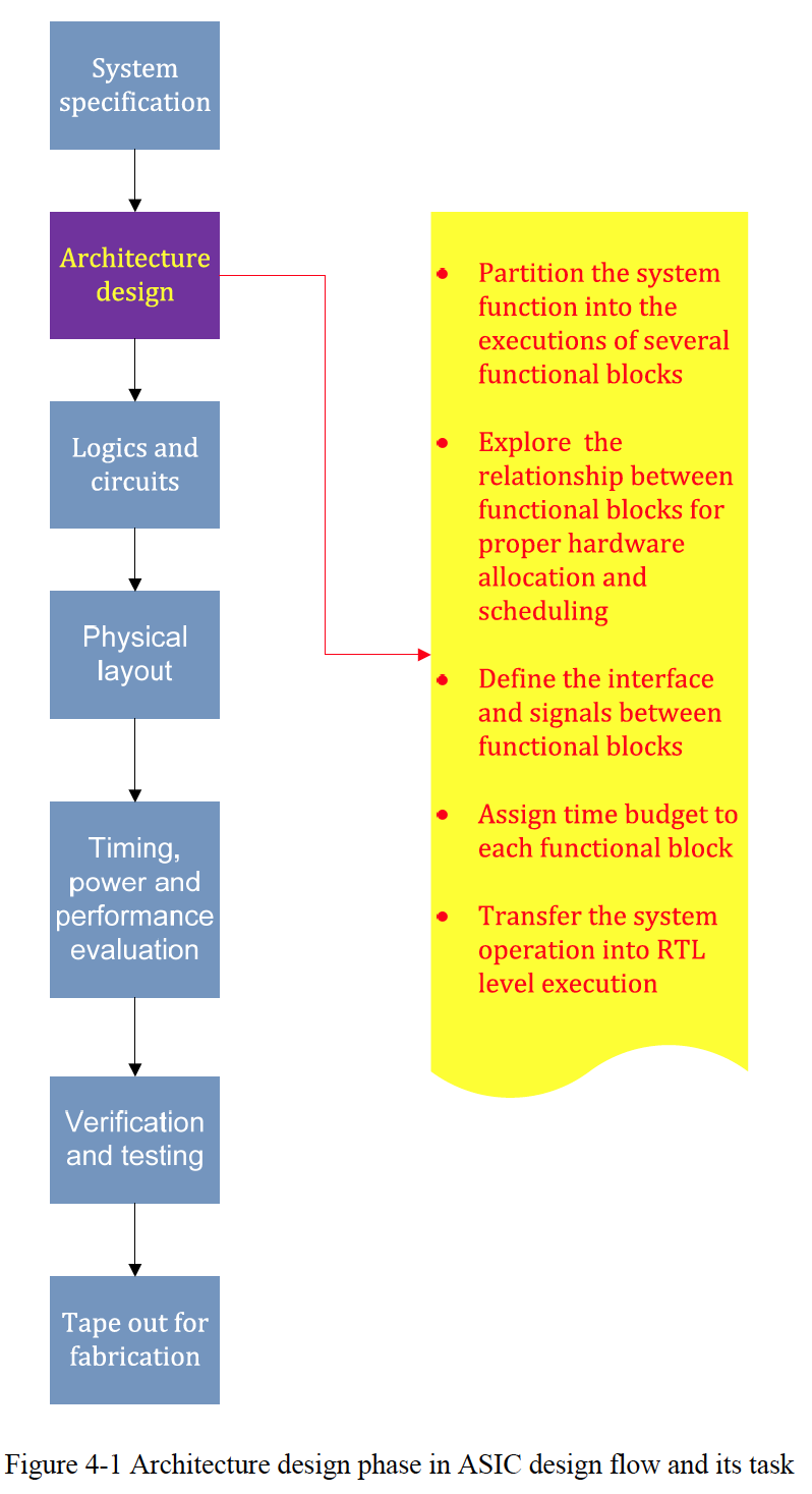
3 What is the architecture of an IC Architecture determines the main functional blocks, their relationship with each other, and more importantly where and when high level operations are performed. Importance A proper architecture is critical to ASIC chip performance and cost. It is perhaps the most important criterion in distinguishing a good design from a poor one. Architecture design relies on the knowledge and experience of a designer, It is still a matter of art that cannot be fully automated by EDA tools. Figure 4 1 indicates the phase of architecture design in the design flow and highlights the involved work.
4
5 At architecture level, functional blocks or Intellectual Properties (IPs) are considered as basic components. In this chapter we shall study how to model and connect these functional blocks. Operations of functional blocks and data flow will be coordinated by a Finite State Machine (FSM). The system architecture is finally described using VHDL (or Verilog) at the RTL level It can be used for a clock cycle-by-cycle simulation, as well as for next phase synthesis and verification. At the end of this chapter, an example architecture of the MSDAP is presented in detail to illustrate architecture development.
6 At the top level, a digital system can be partitioned into two parts: a datapath and a controller. The datapath is used to store, manipulate, and transfer data, and the controller provides the command for these operations. Figure 4 2 illustrates a general datapath structure, where the controller is usually an FSM; ALU is an arithmetic logic unit consisting of an adder, multiplexer and shifter; input/output interface usually is made of shift registers. The memory and bus are used to store and transfer data, respectively.

7
8 In an ASIC architecture each functional block must be defined precisely, including its functionality, input/output pins and signals, as well as the performance requirement in terms of clock cycles. An architecture designer partitions the system function into sub-functions, each of them realized by a functional block. The architecture designer also needs to specify the control signals of each block, which controls the corresponding operation and data flow. In many cases, one has to use the components from a company s existing cell library or IPs from other parties. This adds additional constraints to the architecture design.
9 The objectives of architecture design are twofold: to minimize hardware resources which implement the specified function while satisfying the given performance requirement, and to have a clean partition of the function and a clear relationship between the partitioned sub-functions which facilitates verification and testing.
10 In the single processor structure, the number of ALU units is minimal and other components are added, such as data and coefficient RAMs, and data path controllers. In the previous general datapath structure shown in Figure 4 2, functional blocks are represented at a very high level, and many details are omitted. For instance, the ALU is a general arithmetic logic unit without implementation details. Even for such a simple ALU there might be more than one implementation option.
11 Two possible ALU architectures for the computation of linear convolution A straight forward architecture without specific constraint An architecture with the constraint proposed by the MSDAP

12 A straight forward architecture

13

14

15 An architecture with the constraint
16
17 Parallel properties are explored in the design when a single processor, for instance one ALU, doesn t satisfy the application computation speed requirement. We use a pipeline structure as an example to explore the property of the multiprocessor parallel computation. An example

18
19 How it works
20 Operation details

21

22 Its properties and advantages
23 To demonstrate the structure variety, a slightly different version can be introduced as shown in Figure 4 6.

24 Speed-up obtained by parallel structure
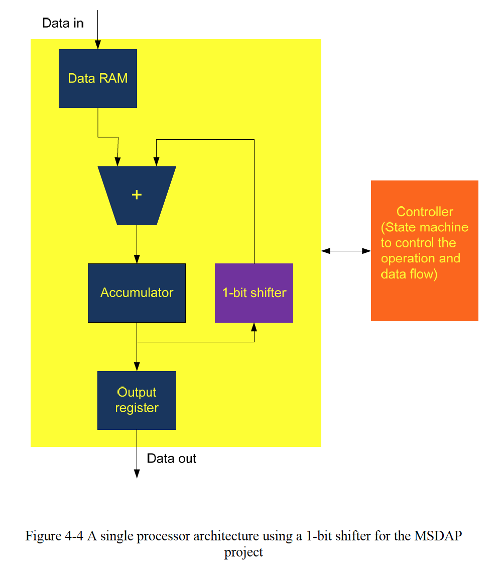
25 The choice between single and multi-processor structure will mainly be determined by the cost, provided that both can accomplish the specified task. For instance, the MSDAP project not only uses a single processor structure, but further uses a 1-bit shifter to reduce the cost, because today s IC speeds can easily satisfy such computation needs.
26 We have seen that the datapath structure consisted of functional blocks as the basic circuit elements. In real design practice, the complexity of these functional blocks may vary from a simple adder to a powerful microprocessor, such as an ARM core in some ASIC designs. Regardless of whether it is a simple or a complex functional block, it needs to be completely defined in a similar way as we define a normal ASIC chip.
27 The definition should include the following basic information: Functionality Input/output pins Signals Interface requirements Layout area and shape specifications Performance requirements Other requirements depending on the application settings

28 A general view of a functional block

29 In electronic design one can use the existing functional block provided by the third party, called semiconductor intellectual property core, IP core, or IP block. This is a reusable unit of logic, cell, or chip layout design that is the intellectual property of another party. The term is derived from the licensing of the patent and source code copyright intellectual property rights that concern the design. IP cores are frequently used as building blocks within ASIC chip designs.
30 IP cores in the electronic design industry have had a profound impact on the design of systems on a chip. For instance, ARM cores have been widely used in many cell phones and multimedia applications. By licensing a design multiple times, IP core providers spread the cost of development among multiple chip makers. IP cores are the re-usable functional blocks within the entire IC industry, instead of within a single IC company.
31 IP cores for standard processors, interfaces, and internal functions enable chip makers to put more resources into developing the differentiating features of their chips. As a result, chip makers are able to develop new innovations faster.
32 The licensing and use of IP cores in chip design became common practice in the 1990s. The microprocessor cores of ARM Holdings are recognized as some of the first widely licensed IP cores. It has been a popular choice for many digital applications because of its competitive time to market. Using such IPs we can significantly improve design efficiency and product reliability since these IP cores have been optimized and tested.

33 IP cores are typically offered as synthesizable RTL netlists. Synthesizable cores are delivered in a hardware description language such as Verilog or VHDL. These are analogous to high level languages such as C in the field of computer programming. IP cores delivered to chip makers as RTL allow chip designers to modify designs if necessary, though many IP vendors offer no warranty or support for modified designs Thus modifications require extreme caution and detailed verification.
34 IP cores are also sometimes offered as generic gate-level netlists. The netlist is a Boolean-algebra representation of the IP s logical function implemented as generic gates or process specific cells. A gate-level netlist is analogous to an assembly-code listing in the field of computer programming. A netlist gives the IP core vendor reasonable protection against reverse engineering. Both netlist and synthesizable cores are called soft cores, because both allow a synthesis, placement and route (SPR) design flow.
35 The advantage of an IP core implemented as a generic gate is that it is portable to other process technologies, if the technology is compatible. Because different processes might be used to implement the gates in the netlist, the timing of the logic circuit may change. A careful timing analysis, both static and dynamic, should be followed to ensure the correct operation.
 are provided to chip makers in transistor-layout format such as in GDSII (GDSII 2011). Digital IP cores are sometimes offered in a layout format as well.")
36 Analog and mixed-signal logics are generally defined as lower-level physical descriptions. Hence, analog IP (PLLs, DAC, ADC, etc.) are provided to chip makers in transistor-layout format such as in GDSII (GDSII 2011). Digital IP cores are sometimes offered in a layout format as well. Such cores, whether analog or digital, are called hard cores (or hard macros), because the core s application function cannot be meaningfully modified by chip designers. Transistor layouts must obey the target foundry s process design rules, and hence, hard cores delivered for one foundry s process cannot be easily ported to a different process or foundry.
37 Merchant foundry operators offer a variety of hard-macro IP functions built for their own foundry process, helping to ensure customer lock-in. Hard cores, by the nature of their low-level representation, offer better predictability of chip performance in terms of timing performance and area.
38 With the presented specs and signal definitions in Chapter 3 for the MSDAP, we now show an example architecture from the project report (Patel and Hernandez-Garduno 2009). A high level abstraction is presented in Figure 4 8 to facilitate the discussion of defining the functionality of each block. The timing information related to the detail clock is not complete since we still need more detailed structures of ALU to budget the number of operations. Each block is defined as required in Figure 4 7 so that its functionality, input/output, status and control signals are precisely stated.
39

40 Definition of the function blocks in the architecture
41 Control logic definition The main function of the Control Logic of the MSDAP is described in Chapter 3 when discussing the system mode and settings. A sample VHDL code has been developed which handles the state transitions. In addition, this Control Logic handles all data transfers and memory reads and writes. It also handles trivial operations such as sign extension and shift operations. For this reason, other components in the MSDAP architecture are designed as asynchronous elements which are able to start their function within 1 Sclk cycle. The Control Logic also completes the task of monitoring and updating top level control signals as specified by the MSDAP specification (the operation mode in Figure 3-7, and signal format and waveform at Section 3.5.2).
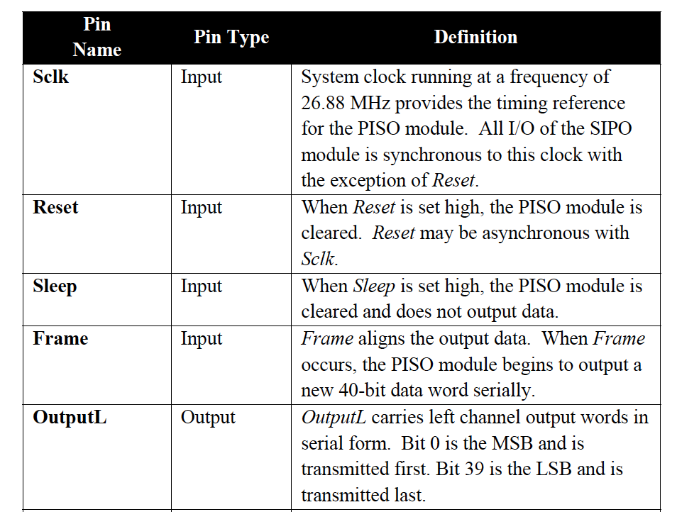
42 SIPO definition The SIPO module is the front-end data interface of the MSDAP that takes 1-bit serial data synchronous to a Data Clock and converts it to 16-bit parallel data. New input words are signaled by an increase in the Frame signal on the first bit of the serial frame and output words are signaled ready by an increase in the DataWordReady signal for the clock cycle, so that the word is guaranteed valid. The SIPO module is cleared by an active high Reset signal. Following are its I/Os and data and control signal definitions.

43 SIPO definition (details)
44
45
46 Memory definition
47
48 Adder/Subtracter definition

49
50 Shift operation definition The shifting operation of the MSDAP is performed by the Controller FSM by reassigning the bit positions of the output of the adder when accumulating the final result and thus is not specified as a separate module. The DataOut signal is the final shifted result that is outputted by the PISO module.
51 PISO definition The PISO module is the data interface of the MSDAP that processes 40-bit parallel data outputs serially via a 1-bit port synchronous to Sclk upon the arrival of the next Frame signal. Output words are signaled ready by an increase of the DataOutValid signal. The OutReady signal is set high for the 40 bits that the PISO is serially outputting data. The SIPO module is cleared by an active high Reset signal and does not output when it receives a high Sleep signal.
52
53
54 From the above example, we see how functional blocks are defined. With a complete definition, blocks can be assigned to different design groups and be verified individually before integrating them into the system. The definition of a function block also includes control signals since a block is controlled by a top level FSM. For instance, a signal Reset is a signal from the Controller FSM that instructs the memory, SIPO and PISO to clear their contents and set them to an initial condition. A functional block also usually feeds the controller information about its status. DataOutValid in the PISO block is such an instance.
55 In a parallel manner, during the architecture development we not only define the functional blocks and corresponding relations, but also assign a time budget to each functional block. Specifically, Each functional block should be given adequate cycles to complete its assigned job; The input to each functional block must be ready when it is needed.
56 Time budget is usually obtained from a process called resource allocation and scheduling. Resource allocation assigns computation tasks to functional blocks, and scheduling arranges these tasks in such a way that they can be executed without confliction. To find the time window for a task to be executed we can use the schedule techniques like as soon as possible and as late as possible. However, combining scheduling with optimal resource allocation is a difficult task. Most of the time, it is still a decision made based on experience.
57 The time budget depends on the proposed architecture and its feasibility must be analyzed carefully in the architecture design stage. A structure is requisite to discussing this topic. In the next section we shall use the architecture of our MSDAP project to show how to allocate the time budget.
58 Figure 4 8 is a top level general datapath architecture, which we have used to assist the discussion of how to define functional blocks. However, architecture should be developed such that it can eventually be coded at an RTL level so that a cycleby-cycle simulation can be carried out to verify the correctness of the digital system without involving detailed logic and circuit designs. The degree of detail depends on the designer, but it must be to a level where we can write VHDL code and verify the hardware design.
59 In doing so, we need to do work similar to what we did in developing the specification of the MSDAP. That is, we need to define the signals and functions among the functional blocks. For example, in referring to the general architecture in Figure 4 8, we do not know how to write the VHDL code since we haven t defined the interfaces between the functional blocks. Therefore, one can t tell in what way ALU works with memory and output interface blocks. In short, too many details are missing there. In the following we look at how to develop such an architecture.
60 Based on the spec, a proposed architecture for the MSDAP is shown in Figure 4 9, which allows us to describe it in VHDL. Only one channel is shown here for clarity. Notice that not all the I/O pins for each functional block have been included. Also, the main controller is shared between the two identical datapath blocks, left and right. (Appendix D presents a complete version of this architecture with all detailed notations and definitions.)

61
62 Definition of each functional block in this architecture are formally presented in the text book. Here is the definition of Data Memory


63

64
65

66

67

68 In this chapter we discussed how to develop an architecture based on the given application. The most popular architecture is a datapath which consists of control logic, input/output, and an ALU unit. These blocks can be further partitioned into smaller functional blocks to facilitate a clear and accurate definition of timing and operation. Such level of detail is necessary for an accurate analysis of timing budget. Final architecture should be described at the RTL level for synthesis and verification.
69 A sample architecture for the MSDAP is given to illustrate the concepts mentioned in the discussion. VHDL codes of the main blocks of the sample architecture are given to show how to accurately describe each functional block without any human language ambiguity, since such code can be simulated for verification. The whole design of the MSDAP, including its architecture, is given in Appendix D, from which the interested reader can have a complete picture of the design process.
70 This chapter also discussed how to explore the parallelism by using multiple processors. The key issue is to properly align the data and operations to obtain the maximum speed-up. The optimal design is if all processors are doing the necessary computations and not being idle. Optimal scheduling and resource allocation is the key for a good architecture. This topic has been studied extensively in high-level synthesis. Readers who are interested in this topic can check the research literatures on this subject and find the state-of-the-art CAD tools to assist architecture design.
71 1. Explain how to define function blocks in architecture design. Try to formalize the method and give an example. 2. Give an example to show how data and computation dependency prevents us from achieving linear speed-up. 3. Summarize the method of architecture development in ASIC design. 4. Synthesizing a behavior model to get an RTL level netlist needs an underlined architecture, for any non-trivial application. Discuss this issue using an example. 5. Discuss why architecture design automation is extremely difficult. Suggest the method to solve this problem. 6. Develop an architecture of the MSDAP. 7. Explain the issue of resource allocation and scheduling in the architecture design. Use the architecture if MSDAP as an example.
Figure 1 FPGA Growth and Usage Trends
 White Paper Avoiding PCB Design Mistakes in FPGA-Based Systems System design using FPGAs is significantly different from the regular ASIC and processor based system design. In this white paper, we will
9/14/2011 14.9.2011 8:38
 Algorithms and Implementation Platforms for Wireless Communications TLT-9706/ TKT-9636 (Seminar Course) BASICS OF FIELD PROGRAMMABLE GATE ARRAYS Waqar Hussain firstname.lastname@tut.fi Department of Computer
Design and Verification of Nine port Network Router
 Design and Verification of Nine port Network Router G. Sri Lakshmi 1, A Ganga Mani 2 1 Assistant Professor, Department of Electronics and Communication Engineering, Pragathi Engineering College, Andhra
Testing of Digital System-on- Chip (SoC)
") Testing of Digital System-on- Chip (SoC) 1 Outline of the Talk Introduction to system-on-chip (SoC) design Approaches to SoC design SoC test requirements and challenges Core test wrapper P1500 core test
Testing of Digital System-on- Chip (SoC) 1 Outline of the Talk Introduction to system-on-chip (SoC) design Approaches to SoC design SoC test requirements and challenges Core test wrapper P1500 core test
Introduction to Digital System Design
 Introduction to Digital System Design Chapter 1 1 Outline 1. Why Digital? 2. Device Technologies 3. System Representation 4. Abstraction 5. Development Tasks 6. Development Flow Chapter 1 2 1. Why Digital
Chapter 2 Logic Gates and Introduction to Computer Architecture
 Chapter 2 Logic Gates and Introduction to Computer Architecture 2.1 Introduction The basic components of an Integrated Circuit (IC) is logic gates which made of transistors, in digital system there are
Aims and Objectives. E 3.05 Digital System Design. Course Syllabus. Course Syllabus (1) Programmable Logic
 Programmable Logic") Aims and Objectives E 3.05 Digital System Design Peter Cheung Department of Electrical & Electronic Engineering Imperial College London URL: www.ee.ic.ac.uk/pcheung/ E-mail: p.cheung@ic.ac.uk How to go
Aims and Objectives E 3.05 Digital System Design Peter Cheung Department of Electrical & Electronic Engineering Imperial College London URL: www.ee.ic.ac.uk/pcheung/ E-mail: p.cheung@ic.ac.uk How to go
MICROPROCESSOR AND MICROCOMPUTER BASICS
 Introduction MICROPROCESSOR AND MICROCOMPUTER BASICS At present there are many types and sizes of computers available. These computers are designed and constructed based on digital and Integrated Circuit
Serial port interface for microcontroller embedded into integrated power meter
 Serial port interface for microcontroller embedded into integrated power meter Mr. Borisav Jovanović, Prof. dr. Predrag Petković, Prof. dr. Milunka Damnjanović, Faculty of Electronic Engineering Nis, Serbia
Switch Fabric Implementation Using Shared Memory
 Order this document by /D Switch Fabric Implementation Using Shared Memory Prepared by: Lakshmi Mandyam and B. Kinney INTRODUCTION Whether it be for the World Wide Web or for an intra office network, today
Architectures and Platforms
 Hardware/Software Codesign Arch&Platf. - 1 Architectures and Platforms 1. Architecture Selection: The Basic Trade-Offs 2. General Purpose vs. Application-Specific Processors 3. Processor Specialisation
DEPARTMENT OF COMPUTER SCIENCE & ENGINEERING Question Bank Subject Name: EC6504 - Microprocessor & Microcontroller Year/Sem : II/IV
 DEPARTMENT OF COMPUTER SCIENCE & ENGINEERING Question Bank Subject Name: EC6504 - Microprocessor & Microcontroller Year/Sem : II/IV UNIT I THE 8086 MICROPROCESSOR 1. What is the purpose of segment registers
Engineering Change Order (ECO) Support in Programmable Logic Design
 Support in Programmable Logic Design") White Paper Engineering Change Order (ECO) Support in Programmable Logic Design A major benefit of programmable logic is that it accommodates changes to the system specification late in the design cycle.
White Paper Engineering Change Order (ECO) Support in Programmable Logic Design A major benefit of programmable logic is that it accommodates changes to the system specification late in the design cycle.
Let s put together a Manual Processor
 Lecture 14 Let s put together a Manual Processor Hardware Lecture 14 Slide 1 The processor Inside every computer there is at least one processor which can take an instruction, some operands and produce
Example-driven Interconnect Synthesis for Heterogeneous Coarse-Grain Reconfigurable Logic
 Example-driven Interconnect Synthesis for Heterogeneous Coarse-Grain Reconfigurable Logic Clifford Wolf, Johann Glaser, Florian Schupfer, Jan Haase, Christoph Grimm Computer Technology /99 Overview Ultra-Low-Power
7a. System-on-chip design and prototyping platforms
 7a. System-on-chip design and prototyping platforms Labros Bisdounis, Ph.D. Department of Computer and Communication Engineering 1 What is System-on-Chip (SoC)? System-on-chip is an integrated circuit
What is a System on a Chip?
 What is a System on a Chip? Integration of a complete system, that until recently consisted of multiple ICs, onto a single IC. CPU PCI DSP SRAM ROM MPEG SoC DRAM System Chips Why? Characteristics: Complex
ARM Microprocessor and ARM-Based Microcontrollers
 ARM Microprocessor and ARM-Based Microcontrollers Nguatem William 24th May 2006 A Microcontroller-Based Embedded System Roadmap 1 Introduction ARM ARM Basics 2 ARM Extensions Thumb Jazelle NEON & DSP Enhancement
ECE410 Design Project Spring 2008 Design and Characterization of a CMOS 8-bit Microprocessor Data Path
 ECE410 Design Project Spring 2008 Design and Characterization of a CMOS 8-bit Microprocessor Data Path Project Summary This project involves the schematic and layout design of an 8-bit microprocessor data
INTRODUCTION TO DIGITAL SYSTEMS. IMPLEMENTATION: MODULES (ICs) AND NETWORKS IMPLEMENTATION OF ALGORITHMS IN HARDWARE
 AND NETWORKS IMPLEMENTATION OF ALGORITHMS IN HARDWARE") INTRODUCTION TO DIGITAL SYSTEMS 1 DESCRIPTION AND DESIGN OF DIGITAL SYSTEMS FORMAL BASIS: SWITCHING ALGEBRA IMPLEMENTATION: MODULES (ICs) AND NETWORKS IMPLEMENTATION OF ALGORITHMS IN HARDWARE COURSE EMPHASIS:
INTRODUCTION TO DIGITAL SYSTEMS 1 DESCRIPTION AND DESIGN OF DIGITAL SYSTEMS FORMAL BASIS: SWITCHING ALGEBRA IMPLEMENTATION: MODULES (ICs) AND NETWORKS IMPLEMENTATION OF ALGORITHMS IN HARDWARE COURSE EMPHASIS:
University of Texas at Dallas. Department of Electrical Engineering. EEDG 6306 - Application Specific Integrated Circuit Design
 University of Texas at Dallas Department of Electrical Engineering EEDG 6306 - Application Specific Integrated Circuit Design Synopsys Tools Tutorial By Zhaori Bi Minghua Li Fall 2014 Table of Contents
Digital Systems Design! Lecture 1 - Introduction!!
 ECE 3401! Digital Systems Design! Lecture 1 - Introduction!! Course Basics Classes: Tu/Th 11-12:15, ITE 127 Instructor Mohammad Tehranipoor Office hours: T 1-2pm, or upon appointments @ ITE 441 Email:
System-on. on-chip Design Flow. Prof. Jouni Tomberg Tampere University of Technology Institute of Digital and Computer Systems. jouni.tomberg@tut.
 System-on on-chip Design Flow Prof. Jouni Tomberg Tampere University of Technology Institute of Digital and Computer Systems jouni.tomberg@tut.fi 26.03.2003 Jouni Tomberg / TUT 1 SoC - How and with whom?
SDLC Controller. Documentation. Design File Formats. Verification
 January 15, 2004 Product Specification 11 Stonewall Court Woodcliff Lake, NJ 07677 USA Phone: +1-201-391-8300 Fax: +1-201-391-8694 E-mail: info@cast-inc.com URL: www.cast-inc.com Features AllianceCORE
System-on-Chip Design with Virtual Components
 FEATURE ARTICLE Thomas Anderson System-on-Chip Design with Virtual Components Here in the Recycling Age, designing for reuse may sound like a great idea. But with increasing requirements and chip sizes,
Digitale Signalverarbeitung mit FPGA (DSF) Soft Core Prozessor NIOS II Stand Mai 2007. Jens Onno Krah
 Soft Core Prozessor NIOS II Stand Mai 2007. Jens Onno Krah") (DSF) Soft Core Prozessor NIOS II Stand Mai 2007 Jens Onno Krah Cologne University of Applied Sciences www.fh-koeln.de jens_onno.krah@fh-koeln.de NIOS II 1 1 What is Nios II? Altera s Second Generation
(DSF) Soft Core Prozessor NIOS II Stand Mai 2007 Jens Onno Krah Cologne University of Applied Sciences www.fh-koeln.de jens_onno.krah@fh-koeln.de NIOS II 1 1 What is Nios II? Altera s Second Generation
1. True or False? A voltage level in the range 0 to 2 volts is interpreted as a binary 1.
 File: chap04, Chapter 04 1. True or False? A voltage level in the range 0 to 2 volts is interpreted as a binary 1. 2. True or False? A gate is a device that accepts a single input signal and produces one
Space product assurance
 ECSS-Q-ST-60-02C Space product assurance ASIC and FPGA development ECSS Secretariat ESA-ESTEC Requirements & Standards Division Noordwijk, The Netherlands Foreword This Standard is one of the series of
Ingar Fredriksen AVR Applications Manager. Tromsø August 12, 2005
 Ingar Fredriksen AVR Applications Manager Tromsø August 12, 2005 Atmel Norway 2005 Atmel Norway 2005 The history of computers Foundation for modern computing 3 An automatic computing machine must have:
CHAPTER 3 Boolean Algebra and Digital Logic
 CHAPTER 3 Boolean Algebra and Digital Logic 3.1 Introduction 121 3.2 Boolean Algebra 122 3.2.1 Boolean Expressions 123 3.2.2 Boolean Identities 124 3.2.3 Simplification of Boolean Expressions 126 3.2.4
Gates, Circuits, and Boolean Algebra
 Gates, Circuits, and Boolean Algebra Computers and Electricity A gate is a device that performs a basic operation on electrical signals Gates are combined into circuits to perform more complicated tasks
Agenda. Michele Taliercio, Il circuito Integrato, Novembre 2001
 Agenda Introduzione Il mercato Dal circuito integrato al System on a Chip (SoC) La progettazione di un SoC La tecnologia Una fabbrica di circuiti integrati 28 How to handle complexity G The engineering
Best Practises for LabVIEW FPGA Design Flow. uk.ni.com ireland.ni.com
 Best Practises for LabVIEW FPGA Design Flow 1 Agenda Overall Application Design Flow Host, Real-Time and FPGA LabVIEW FPGA Architecture Development FPGA Design Flow Common FPGA Architectures Testing and
Simplifying System Design Using the CS4350 PLL DAC
 Simplifying System Design Using the CS4350 PLL 1. INTRODUCTION Typical Digital to Analog Converters (s) require a high-speed Master Clock to clock their digital filters and modulators, as well as some
EEM870 Embedded System and Experiment Lecture 1: SoC Design Overview
 EEM870 Embedded System and Experiment Lecture 1: SoC Design Overview Wen-Yen Lin, Ph.D. Department of Electrical Engineering Chang Gung University Email: wylin@mail.cgu.edu.tw Feb. 2013 Course Overview
MICROPROCESSOR. Exclusive for IACE Students www.iace.co.in iacehyd.blogspot.in Ph: 9700077455/422 Page 1
 MICROPROCESSOR A microprocessor incorporates the functions of a computer s central processing unit (CPU) on a single Integrated (IC), or at most a few integrated circuit. It is a multipurpose, programmable
Measurement and Analysis Introduction of ISO7816 (Smart Card)
") Measurement and Analysis Introduction of ISO7816 (Smart Card) ISO 7816 is an international standard related to electronic identification cards with contacts, especially smart cards, managed jointly by
Measurement and Analysis Introduction of ISO7816 (Smart Card) ISO 7816 is an international standard related to electronic identification cards with contacts, especially smart cards, managed jointly by
Quartus II Software Design Series : Foundation. Digitale Signalverarbeitung mit FPGA. Digitale Signalverarbeitung mit FPGA (DSF) Quartus II 1
 Quartus II 1") (DSF) Quartus II Stand: Mai 2007 Jens Onno Krah Cologne University of Applied Sciences www.fh-koeln.de jens_onno.krah@fh-koeln.de Quartus II 1 Quartus II Software Design Series : Foundation 2007 Altera
(DSF) Quartus II Stand: Mai 2007 Jens Onno Krah Cologne University of Applied Sciences www.fh-koeln.de jens_onno.krah@fh-koeln.de Quartus II 1 Quartus II Software Design Series : Foundation 2007 Altera
High-Level Synthesis for FPGA Designs
 High-Level Synthesis for FPGA Designs BRINGING BRINGING YOU YOU THE THE NEXT NEXT LEVEL LEVEL IN IN EMBEDDED EMBEDDED DEVELOPMENT DEVELOPMENT Frank de Bont Trainer consultant Cereslaan 10b 5384 VT Heesch
Academic year: 2015/2016 Code: IES-1-307-s ECTS credits: 6. Field of study: Electronics and Telecommunications Specialty: -
 Module name: Digital Electronics and Programmable Devices Academic year: 2015/2016 Code: IES-1-307-s ECTS credits: 6 Faculty of: Computer Science, Electronics and Telecommunications Field of study: Electronics
Universal Flash Storage: Mobilize Your Data
 White Paper Universal Flash Storage: Mobilize Your Data Executive Summary The explosive growth in portable devices over the past decade continues to challenge manufacturers wishing to add memory to their
AES1. Ultra-Compact Advanced Encryption Standard Core. General Description. Base Core Features. Symbol. Applications
 General Description The AES core implements Rijndael encoding and decoding in compliance with the NIST Advanced Encryption Standard. Basic core is very small (start at 800 Actel tiles). Enhanced versions
Modeling Sequential Elements with Verilog. Prof. Chien-Nan Liu TEL: 03-4227151 ext:34534 Email: jimmy@ee.ncu.edu.tw. Sequential Circuit
 Modeling Sequential Elements with Verilog Prof. Chien-Nan Liu TEL: 03-4227151 ext:34534 Email: jimmy@ee.ncu.edu.tw 4-1 Sequential Circuit Outputs are functions of inputs and present states of storage elements
Design of a High Speed Communications Link Using Field Programmable Gate Arrays
 Customer-Authored Application Note AC103 Design of a High Speed Communications Link Using Field Programmable Gate Arrays Amy Lovelace, Technical Staff Engineer Alcatel Network Systems Introduction A communication
Chapter 13. PIC Family Microcontroller
 Chapter 13 PIC Family Microcontroller Lesson 01 PIC Characteristics and Examples PIC microcontroller characteristics Power-on reset Brown out reset Simplified instruction set High speed execution Up to
VHDL GUIDELINES FOR SYNTHESIS
 VHDL GUIDELINES FOR SYNTHESIS Claudio Talarico For internal use only 1/19 BASICS VHDL VHDL (Very high speed integrated circuit Hardware Description Language) is a hardware description language that allows
Programmable Logic Controller PLC
 Programmable Logic Controller PLC UPCO ICAI Departamento de Electrónica y Automática 1 PLC Definition PLC is a user friendly, microprocessor based, specialized computer that carries out control functions
ESP-CV Custom Design Formal Equivalence Checking Based on Symbolic Simulation
 Datasheet -CV Custom Design Formal Equivalence Checking Based on Symbolic Simulation Overview -CV is an equivalence checker for full custom designs. It enables efficient comparison of a reference design
ARM Webinar series. ARM Based SoC. Abey Thomas
 ARM Webinar series ARM Based SoC Verification Abey Thomas Agenda About ARM and ARM IP ARM based SoC Verification challenges Verification planning and strategy IP Connectivity verification Performance verification
AND8336. Design Examples of On Board Dual Supply Voltage Logic Translators. Prepared by: Jim Lepkowski ON Semiconductor. http://onsemi.
 Design Examples of On Board Dual Supply Voltage Logic Translators Prepared by: Jim Lepkowski ON Semiconductor Introduction Logic translators can be used to connect ICs together that are located on the
Counters and Decoders
 Physics 3330 Experiment #10 Fall 1999 Purpose Counters and Decoders In this experiment, you will design and construct a 4-bit ripple-through decade counter with a decimal read-out display. Such a counter
Getting the Most Out of Synthesis
 Outline Getting the Most Out of Synthesis Dr. Paul D. Franzon 1. Timing Optimization Approaches 2. Area Optimization Approaches 3. Design Partitioning References 1. Smith and Franzon, Chapter 11 2. D.Smith,
Chapter 4 Register Transfer and Microoperations. Section 4.1 Register Transfer Language
 Chapter 4 Register Transfer and Microoperations Section 4.1 Register Transfer Language Digital systems are composed of modules that are constructed from digital components, such as registers, decoders,
Testing & Verification of Digital Circuits ECE/CS 5745/6745. Hardware Verification using Symbolic Computation
 Testing & Verification of Digital Circuits ECE/CS 5745/6745 Hardware Verification using Symbolic Computation Instructor: Priyank Kalla (kalla@ece.utah.edu) 3 Credits Mon, Wed, 1:25-2:45pm, WEB L105 Office
Lab 1: Full Adder 0.0
 Lab 1: Full Adder 0.0 Introduction In this lab you will design a simple digital circuit called a full adder. You will then use logic gates to draw a schematic for the circuit. Finally, you will verify
Modeling Latches and Flip-flops
 Lab Workbook Introduction Sequential circuits are digital circuits in which the output depends not only on the present input (like combinatorial circuits), but also on the past sequence of inputs. In effect,
A New Paradigm for Synchronous State Machine Design in Verilog
 A New Paradigm for Synchronous State Machine Design in Verilog Randy Nuss Copyright 1999 Idea Consulting Introduction Synchronous State Machines are one of the most common building blocks in modern digital
FPGA. AT6000 FPGAs. Application Note AT6000 FPGAs. 3x3 Convolver with Run-Time Reconfigurable Vector Multiplier in Atmel AT6000 FPGAs.
 3x3 Convolver with Run-Time Reconfigurable Vector Multiplier in Atmel AT6000 s Introduction Convolution is one of the basic and most common operations in both analog and digital domain signal processing.
Computer organization
 Computer organization Computer design an application of digital logic design procedures Computer = processing unit + memory system Processing unit = control + datapath Control = finite state machine inputs
Open Architecture Design for GPS Applications Yves Théroux, BAE Systems Canada
 Open Architecture Design for GPS Applications Yves Théroux, BAE Systems Canada BIOGRAPHY Yves Théroux, a Project Engineer with BAE Systems Canada (BSC) has eight years of experience in the design, qualification,
VHDL-Testbench as Executable Specification
 VHDL- as Executable Specification Michael Pichler Zentrum für Mikroelektronik Aargau Fachhochschule Aargau, Steinackerstrasse 5, CH-5210 Windisch Web: www.zma.ch - E-mail: m.pichler@zma.ch Seite 1 Overview
Power Reduction Techniques in the SoC Clock Network. Clock Power
 Power Reduction Techniques in the SoC Network Low Power Design for SoCs ASIC Tutorial SoC.1 Power Why clock power is important/large» Generally the signal with the highest frequency» Typically drives a
AUTOMATIC NIGHT LAMP WITH MORNING ALARM USING MICROPROCESSOR
 AUTOMATIC NIGHT LAMP WITH MORNING ALARM USING MICROPROCESSOR INTRODUCTION This Project "Automatic Night Lamp with Morning Alarm" was developed using Microprocessor. It is the Heart of the system. The sensors
ECE232: Hardware Organization and Design. Part 3: Verilog Tutorial. http://www.ecs.umass.edu/ece/ece232/ Basic Verilog
 ECE232: Hardware Organization and Design Part 3: Verilog Tutorial http://www.ecs.umass.edu/ece/ece232/ Basic Verilog module ();
DDS. 16-bit Direct Digital Synthesizer / Periodic waveform generator Rev. 1.4. Key Design Features. Block Diagram. Generic Parameters.
 Key Design Features Block Diagram Synthesizable, technology independent VHDL IP Core 16-bit signed output samples 32-bit phase accumulator (tuning word) 32-bit phase shift feature Phase resolution of 2π/2
KEEP IT SYNPLE STUPID
 Utilizing Programmable Logic for Analyzing Hardware Targets Dmitry Nedospasov SHORT DESCRIPTION Hardware security analysis differs from software security analysis primarily in the tools
Module-I Lecture-I Introduction to Digital VLSI Design Flow
 Design Verification and Test of Digital VLSI Circuits NPTEL Video Course Module-I Lecture-I Introduction to Digital VLSI Design Flow Introduction The functionality of electronics equipments and gadgets
Systems on Chip Design
 Systems on Chip Design College: Engineering Department: Electrical First: Course Definition, a Summary: 1 Course Code: EE 19 Units: 3 credit hrs 3 Level: 3 rd 4 Prerequisite: Basic knowledge of microprocessor/microcontroller
Qsys and IP Core Integration
 Qsys and IP Core Integration Prof. David Lariviere Columbia University Spring 2014 Overview What are IP Cores? Altera Design Tools for using and integrating IP Cores Overview of various IP Core Interconnect
Software Defined Radio Architecture for NASA s Space Communications
 From July 2007 High Frequency Electronics Copyright 2007 Summit Technical Media Software Defined Radio Architecture for NASA s Space Communications By Maximilian C. Scardelletti, Richard C. Reinhart, Monty
CISC, RISC, and DSP Microprocessors
 CISC, RISC, and DSP Microprocessors Douglas L. Jones ECE 497 Spring 2000 4/6/00 CISC, RISC, and DSP D.L. Jones 1 Outline Microprocessors circa 1984 RISC vs. CISC Microprocessors circa 1999 Perspective:
150127-Microprocessor & Assembly Language
 Chapter 3 Z80 Microprocessor Architecture The Z 80 is one of the most talented 8 bit microprocessors, and many microprocessor-based systems are designed around the Z80. The Z80 microprocessor needs an
Implementation Details
 LEON3-FT Processor System Scan-I/F FT FT Add-on Add-on 2 2 kbyte kbyte I- I- Cache Cache Scan Scan Test Test UART UART 0 0 UART UART 1 1 Serial 0 Serial 1 EJTAG LEON_3FT LEON_3FT Core Core 8 Reg. Windows
State-of-Art (SoA) System-on-Chip (SoC) Design HPC SoC Workshop
 System-on-Chip (SoC) Design HPC SoC Workshop") Photos placed in horizontal position with even amount of white space between photos and header State-of-Art (SoA) System-on-Chip (SoC) Design HPC SoC Workshop Michael Holmes Manager, Mixed Signal ASIC/SoC
Photos placed in horizontal position with even amount of white space between photos and header State-of-Art (SoA) System-on-Chip (SoC) Design HPC SoC Workshop Michael Holmes Manager, Mixed Signal ASIC/SoC
ETEC 2301 Programmable Logic Devices. Chapter 10 Counters. Shawnee State University Department of Industrial and Engineering Technologies
 ETEC 2301 Programmable Logic Devices Chapter 10 Counters Shawnee State University Department of Industrial and Engineering Technologies Copyright 2007 by Janna B. Gallaher Asynchronous Counter Operation
Concept Engineering Adds JavaScript-based Web Capabilities to Nlview at DAC 2016
 KAL - Large IP Cores: Memory Controllers: SD/SDIO 2.0/3.0 Controller SDRAM Controller DDR/DDR2/DDR3 SDRAM Controller NAND Flash Controller Flash/EEPROM/SRAM Controller Dear , Concept Engineering
RAPID PROTOTYPING OF DIGITAL SYSTEMS Second Edition
 RAPID PROTOTYPING OF DIGITAL SYSTEMS Second Edition A Tutorial Approach James O. Hamblen Georgia Institute of Technology Michael D. Furman Georgia Institute of Technology KLUWER ACADEMIC PUBLISHERS Boston
Computer Systems Design and Architecture by V. Heuring and H. Jordan
 1-1 Chapter 1 - The General Purpose Machine Computer Systems Design and Architecture Vincent P. Heuring and Harry F. Jordan Department of Electrical and Computer Engineering University of Colorado - Boulder
A Verilog HDL Test Bench Primer Application Note
 A Verilog HDL Test Bench Primer Application Note Table of Contents Introduction...1 Overview...1 The Device Under Test (D.U.T.)...1 The Test Bench...1 Instantiations...2 Figure 1- DUT Instantiation...2
CHAPTER 7: The CPU and Memory
 CHAPTER 7: The CPU and Memory The Architecture of Computer Hardware, Systems Software & Networking: An Information Technology Approach 4th Edition, Irv Englander John Wiley and Sons 2010 PowerPoint slides
Codesign: The World Of Practice
 Codesign: The World Of Practice D. Sreenivasa Rao Senior Manager, System Level Integration Group Analog Devices Inc. May 2007 Analog Devices Inc. ADI is focused on high-end signal processing chips and
A Second Undergraduate Course in Digital Logic Design: The Datapath+Controller-Based Approach
 A Second Undergraduate Course in Digital Logic Design: The Datapath+Controller-Based Approach Mitchell A. Thornton 1 and Aaron S. Collins 2 Abstract A second undergraduate course in digital logic design
(Refer Slide Time: 00:01:16 min)
") Digital Computer Organization Prof. P. K. Biswas Department of Electronic & Electrical Communication Engineering Indian Institute of Technology, Kharagpur Lecture No. # 04 CPU Design: Tirning & Control
Digital Computer Organization Prof. P. K. Biswas Department of Electronic & Electrical Communication Engineering Indian Institute of Technology, Kharagpur Lecture No. # 04 CPU Design: Tirning & Control
Manchester Encoder-Decoder for Xilinx CPLDs
 Application Note: CoolRunner CPLDs R XAPP339 (v.3) October, 22 Manchester Encoder-Decoder for Xilinx CPLDs Summary This application note provides a functional description of VHDL and Verilog source code
Traditional IBM Mainframe Operating Principles
 C H A P T E R 1 7 Traditional IBM Mainframe Operating Principles WHEN YOU FINISH READING THIS CHAPTER YOU SHOULD BE ABLE TO: Distinguish between an absolute address and a relative address. Briefly explain
Modeling a GPS Receiver Using SystemC
 Modeling a GPS Receiver using SystemC Modeling a GPS Receiver Using SystemC Bernhard Niemann Reiner Büttner Martin Speitel http://www.iis.fhg.de http://www.iis.fhg.de/kursbuch/kurse/systemc.html The e
FPGA Implementation of RSA Encryption Engine with Flexible Key Size
 FPGA Implementation of RSA Encryption Engine with Flexible Key Size Muhammad I. Ibrahimy, Mamun B.I. Reaz, Khandaker Asaduzzaman and Sazzad Hussain Abstract An approach to develop the FPGA of a flexible
Digital Electronics Detailed Outline
 Digital Electronics Detailed Outline Unit 1: Fundamentals of Analog and Digital Electronics (32 Total Days) Lesson 1.1: Foundations and the Board Game Counter (9 days) 1. Safety is an important concept
W a d i a D i g i t a l
 Wadia Decoding Computer Overview A Definition What is a Decoding Computer? The Wadia Decoding Computer is a small form factor digital-to-analog converter with digital pre-amplifier capabilities. It is
Lab 1: Introduction to Xilinx ISE Tutorial
 Lab 1: Introduction to Xilinx ISE Tutorial This tutorial will introduce the reader to the Xilinx ISE software. Stepby-step instructions will be given to guide the reader through generating a project, creating
VHDL DESIGN OF EDUCATIONAL, MODERN AND OPEN- ARCHITECTURE CPU
 VHDL DESIGN OF EDUCATIONAL, MODERN AND OPEN- ARCHITECTURE CPU Martin Straka Doctoral Degree Programme (1), FIT BUT E-mail: strakam@fit.vutbr.cz Supervised by: Zdeněk Kotásek E-mail: kotasek@fit.vutbr.cz
White Paper Utilizing Leveling Techniques in DDR3 SDRAM Memory Interfaces
 White Paper Introduction The DDR3 SDRAM memory architectures support higher bandwidths with bus rates of 600 Mbps to 1.6 Gbps (300 to 800 MHz), 1.5V operation for lower power, and higher densities of 2
List of courses MEngg (Computer Systems)
") List of courses MEngg (Computer Systems) Course No. Course Title Non-Credit Courses CS-401 CS-402 CS-403 CS-404 CS-405 CS-406 Introduction to Programming Systems Design System Design using Microprocessors
List of courses MEngg (Computer Systems) Course No. Course Title Non-Credit Courses CS-401 CS-402 CS-403 CS-404 CS-405 CS-406 Introduction to Programming Systems Design System Design using Microprocessors
Computer Organization
 Computer Organization and Architecture Designing for Performance Ninth Edition William Stallings International Edition contributions by R. Mohan National Institute of Technology, Tiruchirappalli PEARSON
International Journal of Electronics and Computer Science Engineering 1482
 International Journal of Electronics and Computer Science Engineering 1482 Available Online at www.ijecse.org ISSN- 2277-1956 Behavioral Analysis of Different ALU Architectures G.V.V.S.R.Krishna Assistant
DESIGN AND VERIFICATION OF LSR OF THE MPLS NETWORK USING VHDL
 IJVD: 3(1), 2012, pp. 15-20 DESIGN AND VERIFICATION OF LSR OF THE MPLS NETWORK USING VHDL Suvarna A. Jadhav 1 and U.L. Bombale 2 1,2 Department of Technology Shivaji university, Kolhapur, 1 E-mail: suvarna_jadhav@rediffmail.com
Chapter 13: Verification
 Chapter 13: Verification Prof. Ming-Bo Lin Department of Electronic Engineering National Taiwan University of Science and Technology Digital System Designs and Practices Using Verilog HDL and FPGAs @ 2008-2010,
ARM Cortex-A9 MPCore Multicore Processor Hierarchical Implementation with IC Compiler
 ARM Cortex-A9 MPCore Multicore Processor Hierarchical Implementation with IC Compiler DAC 2008 Philip Watson Philip Watson Implementation Environment Program Manager ARM Ltd Background - Who Are We? Processor
COMBINATIONAL and SEQUENTIAL LOGIC CIRCUITS Hardware implementation and software design
 PH-315 COMINATIONAL and SEUENTIAL LOGIC CIRCUITS Hardware implementation and software design A La Rosa I PURPOSE: To familiarize with combinational and sequential logic circuits Combinational circuits
Efficient Teaching of Digital Design with Automated Assessment and Feedback
 Efficient Teaching of Digital Design with Automated Assessment and Feedback 1 Paul W. Nutter, Member, IEEE, 2 Vasilis F. Pavlidis, Member, IEEE, and 2 Jeffrey Pepper 1 Nano Engineering and Storage Technology