MFM: AFM with magnetical probe magnetic force microscope, Measure magnetic domains combine with topography
|
|
|
- Barnaby Woods
- 7 years ago
- Views:
Transcription
1

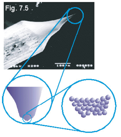
2 STM: scanning tunneling microscope tunneling of electrons between probe and surface, Resolve individual atoms, measure electrical, properties, induce photo luminesence. Only conducting samples. AFM: atomic force microscope Resolution limit ~STM, but more difficult to achieve. Any sample type. MFM: AFM with magnetical probe magnetic force microscope, Measure magnetic domains combine with topography In some cases can image individual Molecules - Å level resolution Many artifacts are possible! Some limitations on the types of samples that may be imaged. Relatively Inexpensive ($50K-$200K) & easy to learn difficult to master y x
3 SPM scanners are made from a piezoelectric material that expands and contracts proportionally to an applied voltage. Whether they expand or contract depends upon the polarity of the applied voltage. Digital Instruments scanners have AC voltage ranges of +220 to -220V. 0 V - V + V No applied voltage Contracted Extended In some versions, the piezo tube moves the sample relative to the tip. In other models, the sample is stationary while the scanner moves the tip. AC signals applied to conductive areas of the tube create piezo movement along the three major axes.


4 '&&&'''&! "# $! % &


5

6

7 !"# $%" ( ) *+ ( *+ (,, *+ -

8

9 & ' (

10 ) *!"# $ &&& &+
11 *, *, photodiode laser AFM probe scans over the surface (in contact) probe piezo-element


12 *, *, The atomic force microscope measures topography with a force probe Cantilever touching a sample Optical lever Tube scanner measures 24 mm in diameter, while the cantilever is 100 µm long.
13 *, *, photodiode laser piezo x z y cantilever cantilever tip
14 *, *, AFMs use feedback to regulate the force on the sample The AFM feedback loop. A compensation network (which in AFM is a computer program) monitors the cantilever deflection and keeps it constant by adjusting the height of the sample (or cantilever).
15
16
17 *, *, The presence of a feedback loop is one of the subtler differences between AFMs and older stylus-based instruments such as record players and stylus profilometers. The AFM not only measures the force on the sample but also regulates it, allowing acquisition of images at very low forces. The feedback loop (figure 6) consists of the tube scanner that controls the height of the entire sample; the cantilever and optical lever, which measures the local height of the sample; and a feedback circuit that attempts to keep the cantilever deflection constant by adjusting the voltage applied to the scanner. One point of interest: the faster the feedback loop can correct deviations of the cantilever deflection, the faster the AFM can acquire images; therefore, a well-constructed feedback loop is essential to microscope performance. AFM feedback loops tend to have a bandwidth of about 10 khz, resulting in image acquisition times of about one minute.

18 *,

19 *, SPM tip tipholder sample photodiode fluid in O-ring mirror laser beam fluid cell fluid out piezo translator motor control x,y,z piezo translator sample in air and in buffer solutions
20 &(*, ( AFM tip superhelical DNA plasmid path of AFM tip DNA double helix Mg 2+ Mg 2+ Mg 2+ Mg 2+ Mg 2+ Mg 2+ negatively charged mica surface


21 *,- &./0 0 ( AFM tip

22 *,- &1 *

23 *,- &2 1 1
24 In its repulsive "contact" mode, the instrument lightly touches a tip at the end of a leaf spring or "cantilever" to the sample. As a raster-scan drags the tip over the sample, some sort of detection apparatus measures the vertical deflection of the cantilever, which indicates the local sample height. Thus, in contact mode the AFM measures hard-sphere repulsion forces between the tip and sample. *, *, In noncontact mode, the AFM derives topographic images from measurements of attractive forces; the tip does not touch the sample. AFMs can achieve a resolution of 10 pm, and unlike electron microscopes, can image samples in air and under liquids.
25 2*, A tip is scanned across the sample while a feedback loop maintains a constant cantilever deflection (and force) The tip contacts the surface through the adsorbed fluid layer. Forces range from nano to micro N in ambient conditions and even lower (0.1 nn or less) in liquids.
26 3 *, A cantilever with attached tip is oscillated at its resonant frequency and scanned across the sample surface. A constant oscillation amplitude (and thus a constant tip-sample interaction) are maintained during scanning. Typical amplitudes are nm. Forces can be 200 pn or less The amplitude of the oscillations changes when the tip scans over bumps or depressions on a surface.
27 1 #*, The cantilever is oscillated slightly above its resonant frequency. Oscillations <10nm The tip does not touch the sample. Instead, it oscillates above the adsorbed fluid layer. A constant oscillation amplitude is maintained. The resonant frequency of the cantilever is decreased by the van der Waals forces which extend from 1-10nm above the adsorbed fluid layer. This in turn changes the amplitude of oscillation.
28 Contact Mode Advantages: High scan speeds The only mode that can obtain atomic resolution images Rough samples with extreme changes in topography can sometimes be scanned more easily Disadvantages: * &(4 &*, Lateral (shear) forces can distort features in the image The forces normal to the tip-sample interaction can be high in air due to capillary forces from the adsorbed fluid layer on the sample surface. The combination of lateral forces and high normal forces can result in reduced spatial resolution and may damage soft samples (i.e. biological samples, polymers, silicon) due to scraping
29 * &(4 &*, Tapping Mode AFM Advantages: Higher lateral resolution on most samples (1 to 5nm) Lower forces and less damage to soft samples imaged in air Lateral forces are virtually eliminated so there is no scraping Disadvantages: Slightly lower scan speed than contact mode AFM
30 *, *, In principle, AFM resembles the record player as well as the stylus profilometer. However, AFM incorporates a number of refinements that enable it to achieve atomic-scale resolution: Sensitive detection Flexible cantilevers Sharp tips High-resolution tip-sample positioning Force feedback

31 * &
Lecture 4 Scanning Probe Microscopy (SPM)
") Lecture 4 Scanning Probe Microscopy (SPM) General components of SPM; Tip --- the probe; Cantilever --- the indicator of the tip; Tip-sample interaction --- the feedback system; Scanner --- piezoelectric
Lecture 4 Scanning Probe Microscopy (SPM) General components of SPM; Tip --- the probe; Cantilever --- the indicator of the tip; Tip-sample interaction --- the feedback system; Scanner --- piezoelectric
STM and AFM Tutorial. Katie Mitchell January 20, 2010
 STM and AFM Tutorial Katie Mitchell January 20, 2010 Overview Scanning Probe Microscopes Scanning Tunneling Microscopy (STM) Atomic Force Microscopy (AFM) Contact AFM Non-contact AFM RHK UHV350 AFM/STM
Keysight Technologies How to Choose your MAC Lever. Technical Overview
 Keysight Technologies How to Choose your MAC Lever Technical Overview Introduction Atomic force microscopy (AFM) is a sub-nanometer scale imaging and measurement tool that can be used to determine a sample
Atomic Force Microscopy. Long Phan Nanotechnology Summer Series May 15, 2013
 Atomic Force Microscopy Long Phan Nanotechnology Summer Series May 15, 2013 1 World s Smallest Movie 2 Outline What is AFM? How does AFM Work? 3 Modes: Contact mode Non contact mode Tapping mode Imaging
Scanning Probe Microscopy
 Ernst Meyer Hans Josef Hug Roland Bennewitz Scanning Probe Microscopy The Lab on a Tip With 117 Figures Mß Springer Contents 1 Introduction to Scanning Probe Microscopy f f.1 Overview 2 f.2 Basic Concepts
ATOMIC FORCE MICROSCOPY
 ATOMIC FORCE MICROSCOPY Introduction The atomic force microscope, or AFM, is a member of the family of instruments known as scanning probe microscopes. The AFM operates under a completely different principle
1 Introduction. 1.1 Historical Perspective
 j1 1 Introduction 1.1 Historical Perspective The invention of scanning probe microscopy is considered one of the major advances in materials science since 1950 [1, 2]. Scanning probe microscopy includes
Piezoelectric Scanners
 Piezoelectric Scanners Piezoelectric materials are ceramics that change dimensions in response to an applied voltage and conversely, they develop an electrical potential in response to mechanical pressure.
Tecniche a scansione di sonda per nanoscopia e nanomanipolazione 2: AFM e derivati
 LS Scienza dei Materiali - a.a. 2008/09 Fisica delle Nanotecnologie part 5.2 Version 7, Nov 2008 Francesco Fuso, tel 0502214305, 0502214293 - fuso@df.unipi.it http://www.df.unipi.it/~fuso/dida Tecniche
(Nano)materials characterization
materials characterization") (Nano)materials characterization MTX9100 Nanomaterials Lecture 8 OUTLINE 1 -What SEM and AFM are good for? - What is the Atomic Force Microscopes Contribution to Nanotechnology? - What is Spectroscopy?
(Nano)materials characterization MTX9100 Nanomaterials Lecture 8 OUTLINE 1 -What SEM and AFM are good for? - What is the Atomic Force Microscopes Contribution to Nanotechnology? - What is Spectroscopy?
INTRODUCTION TO SCANNING TUNNELING MICROSCOPY
 INTRODUCTION TO SCANNING TUNNELING MICROSCOPY SECOND EDITION C. JULIAN CHEN Department of Applied Physics and Applied Mathematics, Columbia University, New York OXJORD UNIVERSITY PRESS Contents Preface
7/3/2014. Introduction to Atomic Force Microscope. Introduction to Scanning Force Microscope. Invention of Atomic Force Microscope (AFM)
") Introduction to Atomic Force Microscope Introduction to Scanning Force Microscope Not that kind of atomic Tien Ming Chuang ( 莊 天 明 ) Institute of Physics, Academia Sinica Tien Ming Chuang ( 莊 天 明 ) Institute
Introduction to Atomic Force Microscope Introduction to Scanning Force Microscope Not that kind of atomic Tien Ming Chuang ( 莊 天 明 ) Institute of Physics, Academia Sinica Tien Ming Chuang ( 莊 天 明 ) Institute
Basic principles and mechanisms of NSOM; Different scanning modes and systems of NSOM; General applications and advantages of NSOM.
 Lecture 16: Near-field Scanning Optical Microscopy (NSOM) Background of NSOM; Basic principles and mechanisms of NSOM; Basic components of a NSOM; Different scanning modes and systems of NSOM; General
Scanning probe microscopy AFM, STM. Near field Scanning Optical Microscopy(NSOM) Scanning probe fabrication
 Scanning probe fabrication") Scanning probe microscopy AFM, STM Near field Scanning Optical Microscopy(NSOM) Scanning probe fabrication Scanning Probe Microscopy 1986 Binning and Rohrer shared Nobel Prize in Physics for invention.stm
Scanning probe microscopy AFM, STM Near field Scanning Optical Microscopy(NSOM) Scanning probe fabrication Scanning Probe Microscopy 1986 Binning and Rohrer shared Nobel Prize in Physics for invention.stm
It has long been a goal to achieve higher spatial resolution in optical imaging and
 Nano-optical Imaging using Scattering Scanning Near-field Optical Microscopy Fehmi Yasin, Advisor: Dr. Markus Raschke, Post-doc: Dr. Gregory Andreev, Graduate Student: Benjamin Pollard Department of Physics,
Atomic Force Microscopy Observation and Characterization of a CD Stamper, Lycopodium Spores, and Step-Height Standard Diffraction Grating
 Atomic Force Microscopy Observation and Characterization of a CD Stamper, Lycopodium Spores, and Step-Height Standard Diffraction Grating Michael McMearty and Frit Miot Special Thanks to Brendan Cross
AFM (Atomic Force Microscope) Instructions
 Instructions") AFM (Atomic Force Microscope) Instructions Contact Mode AFM Advantages: High scan speeds (throughput) Contact mode AFM is the only AFM technique, which can obtain "atomic resolution" images. Rough samples
AFM (Atomic Force Microscope) Instructions Contact Mode AFM Advantages: High scan speeds (throughput) Contact mode AFM is the only AFM technique, which can obtain "atomic resolution" images. Rough samples
Usage of Carbon Nanotubes in Scanning Probe Microscopes as Probe. Keywords: Carbon Nanotube, Scanning Probe Microscope
 International Journal of Arts and Sciences 3(1): 18-26 (2009) CD-ROM. ISSN: 1944-6934 InternationalJournal.org Usage of Carbon Nanotubes in Scanning Probe Microscopes as Probe Bedri Onur Kucukyildirim,
Counting and imaging bacteria using fluorescent microscopy & Electron Microscopy and Atomic Force Microscopy (AFM)
") Counting and imaging bacteria using fluorescent microscopy & Electron Microscopy and Atomic Force Microscopy (AFM) Bruce E. Logan Kappe Professor of Environmental Engineering Department of Civil and Environmental
Counting and imaging bacteria using fluorescent microscopy & Electron Microscopy and Atomic Force Microscopy (AFM) Bruce E. Logan Kappe Professor of Environmental Engineering Department of Civil and Environmental
Atomic Force Microscope Physics Assignment
 Atomic Force Microscope Physics Assignment Group Members: İbrahim Mert DARICI Syed Arslan Afzal HASHMI Ali ZAREI Sudhakar Murthy MOLLI Materials Processing 2006 PHYSICS ASSIGNMENT 1 Content 1 Introduction...
ATOMIC FORCEMICROSCOPYASTOOL INCELLBIOLOGICAL RESEARCH FORGROUNDBASEDANDIN-FLIGHTSTUDIES
 ATOMIC FORCEMICROSCOPYASTOOL INCELLBIOLOGICAL RESEARCH FORGROUNDBASEDANDIN-FLIGHTSTUDIES J.J.W.A vanloon DutchExperimentSupportCenter(DESC),Dept.OralBiology,ACTA- VrijeUniversiteit,Amsterdam,TheNetherlands.
Nano-Spectroscopy. Solutions AFM-Raman, TERS, NSOM Chemical imaging at the nanoscale
 Nano-Spectroscopy Solutions AFM-Raman, TERS, NSOM Chemical imaging at the nanoscale Since its introduction in the early 80 s, Scanning Probe Microscopy (SPM) has quickly made nanoscale imaging an affordable
High flexibility of DNA on short length scales probed by atomic force microscopy
 High flexibility of DNA on short length scales probed by atomic force microscopy Wiggins P. A. et al. Nature Nanotechnology (2006) presented by Anja Schwäger 23.01.2008 Outline Theory/Background Elasticity
Atomic Force Microscope
 Atomic Force Microscope (Veeco Nanoman) User Manual Basic Operation 4 th Edition Aug 2012 NR System Startup If the system is currently ON To start the NanoScope software, double-click the NanoScope startup
Lecture 6 Scanning Tunneling Microscopy (STM) General components of STM; Tunneling current; Feedback system; Tip --- the probe.
 General components of STM; Tunneling current; Feedback system; Tip --- the probe.") Lecture 6 Scanning Tunneling Microscopy (STM) General components of STM; Tunneling current; Feedback system; Tip --- the probe. Brief Overview of STM Inventors of STM The Nobel Prize in Physics 1986 Nobel
Lecture 6 Scanning Tunneling Microscopy (STM) General components of STM; Tunneling current; Feedback system; Tip --- the probe. Brief Overview of STM Inventors of STM The Nobel Prize in Physics 1986 Nobel
Tecniche a scansione di sonda per nanoscopia e nanomanipolazione: STM, AFM e derivati
 LS Scienza dei Materiali - a.a. 2006/07 Fisica delle Nanotecnologie part 5.1 Version 5a, Nov 2006 Francesco Fuso, tel 0502214305, 0502214293 - fuso@df.unipi.it http://www.df.unipi.it/~fuso/dida Tecniche
5. Scanning Near-Field Optical Microscopy 5.1. Resolution of conventional optical microscopy
 5. Scanning Near-Field Optical Microscopy 5.1. Resolution of conventional optical microscopy Resolution of optical microscope is limited by diffraction. Light going through an aperture makes diffraction
Non-Contact Vibration Measurement of Micro-Structures
 Non-Contact Vibration Measurement of Micro-Structures Using Laser Doppler Vibrometry (LDV) and Planar Motion Analysis (PMA) to examine and assess the vibration characteristics of micro- and macro-structures.
Calibration of AFM with virtual standards; robust, versatile and accurate. Richard Koops VSL Dutch Metrology Institute Delft
 Calibration of AFM with virtual standards; robust, versatile and accurate Richard Koops VSL Dutch Metrology Institute Delft 19-11-2015 VSL Dutch Metrology Institute VSL is the national metrology institute
UNIVERSITY OF SOUTHAMPTON. Scanning Near-Field Optical Microscope Characterisation of Microstructured Optical Fibre Devices.
 UNIVERSITY OF SOUTHAMPTON Scanning Near-Field Optical Microscope Characterisation of Microstructured Optical Fibre Devices. Christopher Wyndham John Hillman Submitted for the degree of Doctor of Philosophy
Microscopy. MICROSCOPY Light Electron Tunnelling Atomic Force RESOLVE: => INCREASE CONTRAST BIODIVERSITY I BIOL1051 MAJOR FUNCTIONS OF MICROSCOPES
 BIODIVERSITY I BIOL1051 Microscopy Professor Marc C. Lavoie marc.lavoie@cavehill.uwi.edu MAJOR FUNCTIONS OF MICROSCOPES MAGNIFY RESOLVE: => INCREASE CONTRAST Microscopy 1. Eyepieces 2. Diopter adjustment
Microscopy: Principles and Advances
 Microscopy: Principles and Advances Chandrashekhar V. Kulkarni University of Central Lancashire, Preston, United kingdom May, 2014 University of Ljubljana Academic Background 2005-2008: PhD-Chemical Biology
Atomic Force Microscope and Magnetic Force Microscope Background Information
 Atomic Force Microscope and Magnetic Force Microscope Background Information Lego Building Instructions There are several places to find the building instructions for building the Lego models of atomic
Scanning Near-Field Optical Microscopy for Measuring Materials Properties at the Nanoscale
 Scanning Near-Field Optical Microscopy for Measuring Materials Properties at the Nanoscale Outline Background Research Design Detection of Near-Field Signal Submonolayer Chemical Sensitivity Conclusions
Agilent 5500 AFM. Data Sheet. Features and Benefits
 Agilent 5500 AFM Data Sheet Figure 1. STM image of HOPG showing atomic structure. Scan size: 4 nm. Features and Benefits Exceptional environmental and temperature control Superior scanning in fluids, gases,
SCANNING PROBE MICROSCOPY NANOS-E3 SCHOOL 29/09/2015 An introduction to surface microscopy probes
 SCANNING PROBE MICROSCOPY NANOS-E3 SCHOOL 29/09/2015 An introduction to surface microscopy probes SPM is ubiquitous in modern research Physics Nanotechnology/chemistry Nature Nanotechnology 10, 156 160
A METHOD OF PRECISE CALIBRATION FOR PIEZOELECTRICAL ACTUATORS
 Uludağ Üniversitesi Mühendislik-Mimarlık Fakültesi Dergisi, Cilt 9, Sayı, 24 A METHOD OF PRECISE CALIBRATION FOR PIEZOELECTRICAL ACTUATORS Timur CANEL * Yüksel BEKTÖRE ** Abstract: Piezoelectrical actuators
High Speed Atomic Force Microscopy of Biomolecules by Image Tracking
 Biophysical Journal Volume 77 October 1999 2295 2303 2295 High Speed Atomic Force Microscopy of Biomolecules by Image Tracking S. John T. van Noort, Kees O. van der Werf, Bart G. de Grooth, and Jan Greve
Nano-Microscopy: Lecture 1. Pavel Zinin HIGP, University of Hawaii, Honolulu, USA
 GG 711: Advanced Techniques in Geophysics and Materials Science Nano-Microscopy: Lecture 1 Scanning Tunneling and Atomic Force Microscopies Principles Pavel Zinin HIGP, University of Hawaii, Honolulu,
NEAR FIELD OPTICAL MICROSCOPY AND SPECTROSCOPY WITH STM AND AFM PROBES
 Vol. 93 (1997) A CTA PHYSICA POLONICA A No. 2 Proceedings of the 1st International Symposium on Scanning Probe Spectroscopy and Related Methods, Poznań 1997 NEAR FIELD OPTICAL MICROSCOPY AND SPECTROSCOPY
Microscopie à champs proche: et application
 Microscopie à champs proche: Théorie et application STM, effet tunnel et applications AFM, interactions et applications im2np, Giens 2010 Optical microscopy: resolution limit resolution limit: d min =
Multi-mode Atomic Force Microscope (with High Voltage Piezo Force Microscope and +/- 8000 Oe Variable Field module.)
") Multi-mode Atomic Force Microscope (with High Voltage Piezo Force Microscope and +/- 8000 Oe Variable Field module.) Main specifications of the proposed instrument: 1 Instrument Resolution: 1.1 The instrument
Multi-mode Atomic Force Microscope (with High Voltage Piezo Force Microscope and +/- 8000 Oe Variable Field module.) Main specifications of the proposed instrument: 1 Instrument Resolution: 1.1 The instrument
Surface Profilometry as a tool to Measure Thin Film Stress, A Practical Approach. Gianni Franceschinis, RIT MicroE Graduate Student
 1 Surface Profilometry as a tool to Measure Thin Film Stress, A Practical Approach. Gianni Franceschinis, RIT MicroE Graduate Student Abstract-- As the film decreases in thickness the requirements of more
NP-AFM. Samples as large as 200 x 200 x 20 mm are profiled by the NP-AFM system, and several stage options are available for many types of samples.
 NP-AFM The NP-AFM is a complete nanoprofiler tool including everything required for scanning samples: microscope stage, electronic box, control computer, probes, manuals, and a video microscope. Samples
How To Image A Magnetic Microscope
 Agustina Asenjo Dpto. Propiedades Opticas, Magnéticas y de Transporte Instituto de Ciencia de Materiales de Madrid- CSIC Introducción: Esquema MFM frente a otras técnicas de observación de dominios. Fundamentos
Fast-scanning near-field scanning optical microscopy. using a high-frequency dithering probe
 Fast-scanning near-field scanning optical microscopy using a high-frequency dithering probe Yongho Seo and Wonho Jhe * Center for Near-field Atom-photon Technology and School of Physics, Seoul National
USING CDs AND DVDs AS DIFFRACTION GRATINGS
 USING CDs AND DVDs AS DIFFRACTION GRATINGS Rama Balachandran Riverwood High School Atlanta, GA Karen Porter-Davis Chamblee Charter High School Chamblee, GA Copyright Georgia Institute of Technology 2009
CREOL, College of Optics & Photonics, University of Central Florida
 OSE6650 - Optical Properties of Nanostructured Materials Optical Properties of Nanostructured Materials Fall 2013 Class 3 slide 1 Challenge: excite and detect the near field Thus far: Nanostructured materials
AFM-kit. Development of a kit for building from scratch an educational (but decently performing - i.e. usable) AFM.
 AFM.") AFM-kit Development of a kit for building from scratch an educational (but decently performing - i.e. usable) AFM. Building AFM is the best way to understand how it "really" works. initial tasks Define
AFM-kit Development of a kit for building from scratch an educational (but decently performing - i.e. usable) AFM. Building AFM is the best way to understand how it "really" works. initial tasks Define
Drive an Atomic Force Microscope using LabVIEW software
 Fachhochschule Regensburg Prüfeninger Straße 58 93049 Regensburg DEUTSCHLAND April 2001 June 2001 Drive an Atomic Force Microscope using LabVIEW software Students names: CAMUS Nicolas PERDU Nicolas Professors
nanovea.com MECHANICAL TESTERS Indentation Scratch Wear
 MECHANICAL TESTERS Indentation Scratch Wear nanovea.com MECHANICAL TESTER INTRO Nanovea Mechanical Testers provide unmatched multi-function Nano and Micro/Macro modules on a single platform. Both the Nano
Experiment 5. Lasers and laser mode structure
 Northeastern University, PHYS5318 Spring 2014, 1 1. Introduction Experiment 5. Lasers and laser mode structure The laser is a very important optical tool that has found widespread use in science and industry,
3D TOPOGRAPHY & IMAGE OVERLAY OF PRINTED CIRCUIT BOARD ASSEMBLY
 3D TOPOGRAPHY & IMAGE OVERLAY OF PRINTED CIRCUIT BOARD ASSEMBLY Prepared by Duanjie Li, PhD & Andrea Novitsky 6 Morgan, Ste156, Irvine CA 92618 P: 949.461.9292 F: 949.461.9232 nanovea.com Today's standard
SPM 150 Aarhus with KolibriSensor
 Customied Systems and Solutions Nanostructures and Thin Film Deposition Surface Analysis and Preparation Components Surface Science Applications SPM 150 Aarhus with KolibriSensor Atomic resolution NC-AFM
Scanning Near Field Optical Microscopy: Principle, Instrumentation and Applications
 Scanning Near Field Optical Microscopy: Principle, Instrumentation and Applications Saulius Marcinkevičius Optics, ICT, KTH 1 Outline Optical near field. Principle of scanning near field optical microscope
Near-field scanning optical microscopy (SNOM)
") Adviser: dr. Maja Remškar Institut Jožef Stefan January 2010 1 2 3 4 5 6 Fluorescence Raman and surface enhanced Raman 7 Conventional optical microscopy-limited resolution Two broad classes of techniques
Adviser: dr. Maja Remškar Institut Jožef Stefan January 2010 1 2 3 4 5 6 Fluorescence Raman and surface enhanced Raman 7 Conventional optical microscopy-limited resolution Two broad classes of techniques
MEMS mirror for low cost laser scanners. Ulrich Hofmann
 MEMS mirror for low cost laser scanners Ulrich Hofmann Outline Introduction Optical concept of the LIDAR laser scanner MEMS mirror requirements MEMS mirror concept, simulation and design fabrication process
Subject Area(s) Biology. Associated Unit Engineering Nature: DNA Visualization and Manipulation. Associated Lesson Imaging the DNA Structure
 Biology. Associated Unit Engineering Nature: DNA Visualization and Manipulation. Associated Lesson Imaging the DNA Structure") Subject Area(s) Biology Associated Unit Engineering Nature: DNA Visualization and Manipulation Associated Lesson Imaging the DNA Structure Activity Title Inside the DNA Header Image 1 ADA Description:
Subject Area(s) Biology Associated Unit Engineering Nature: DNA Visualization and Manipulation Associated Lesson Imaging the DNA Structure Activity Title Inside the DNA Header Image 1 ADA Description:
Characterization of surfaces by AFM topographical, mechanical and chemical properties
 Characterization of surfaces by AFM topographical, mechanical and chemical properties Jouko Peltonen Department of physical chemistry Åbo Akademi University Atomic Force Microscopy (AFM) Contact mode AFM
Atomic Force Microscopy - Basics and Applications
 Astrid Kronenberger School of Engineering and Science Atomic Force Microscopy - Basics and Applications Summer School June 2006 Complex Materials: Cooperative Projects of the Natural, Engineering and Biosciences
E_mail: afmproject@free.fr
 Décines - France Student team : PORCHER Nicolas ROMEU Guillaume TISSOT François Teacher : JEANJACQUOT Philippe E_mail: afmproject@free.fr Picture gallery 2 Summary A nanometric picture for a nanometric
3D Raman Imaging Nearfield-Raman TERS. Solutions for High-Resolution Confocal Raman Microscopy. www.witec.de
 3D Raman Imaging Nearfield-Raman TERS Solutions for High-Resolution Confocal Raman Microscopy www.witec.de 01 3D Confocal Raman Imaging Outstanding performance in speed, sensitivity, and resolution with
FRT - setting the standard
 FRT - setting the standard Surface Analysis Metrology Instruments Process Control Chromatic white light sensor Weißlicht Specs: Linse blauer Fokus roter Fokus max height range 300 µm 600 µm 3 mm 10 mm
ENGINEERING METROLOGY
 ENGINEERING METROLOGY ACADEMIC YEAR 92-93, SEMESTER ONE COORDINATE MEASURING MACHINES OPTICAL MEASUREMENT SYSTEMS; DEPARTMENT OF MECHANICAL ENGINEERING ISFAHAN UNIVERSITY OF TECHNOLOGY Coordinate Measuring
Force Spectroscopy with the Atomic Force Microscope
 Force Spectroscopy with the Atomic Force Microscope Application Note Wenhai Han, Agilent Technologies F. Michael Serry Figure 1. In Force spectroscopy raster-scanning is disabled temporarily or indefinitely
Review of Scientific Paper Contact Electrification Using Force Microcopy
 Volume 1 Number 1 1 Review of Scientific Paper Contact Electrification Using Force Microcopy Joel-Anthony Gray, B.S.E.E. Nanoscience Minor - University of Texas at Dallas. Abstract Charge exchange is a
Radiant Dyes Laser Accessories GmbH
 New NarrowScan New Resonator Design Improved Sine Drive Unit Autotracking Frequency doubling, tripling and mixing Wavelength Separation Unit Frequency Stabilization Temperature Stabilization Wavelength
Sensors & Instruments for station. returned samples. Chun Chia Tan
 Sensors & Instruments for station based materials characterization of returned samples Chun Chia Tan 04/01/2009 Outline Introduction to materials characterization General overview of the equipment used
Surface Analysis with STM and AFM
 Sergei N. Magonov, Myung-Hwan Whangbo Surface Analysis with STM and AFM Experimental and Theoretical Aspects of Image Analysis VCH Weinheim New York Basel Cambridge Tokyo Preface V 1 Introduction 1 1.1
Mechanical and electrical investigations of thin polymer films by variabletemperature force microscopy
 Mechanical and electrical investigations of thin polymer films by variabletemperature force microscopy Dissertation zur Erlangung des Doktorgrades Dr. rer. nat. der Fakultät für Naturwissenschaften der
Use the BET (after Brunauer, Emmett and Teller) equation is used to give specific surface area from the adsorption
 equation is used to give specific surface area from the adsorption") Number of moles of N 2 in 0.129dm 3 = 0.129/22.4 = 5.76 X 10⁻³ moles of N 2 gas Module 8 : Surface Chemistry Objectives Lecture 37 : Surface Characterization Techniques After studying this lecture, you
Number of moles of N 2 in 0.129dm 3 = 0.129/22.4 = 5.76 X 10⁻³ moles of N 2 gas Module 8 : Surface Chemistry Objectives Lecture 37 : Surface Characterization Techniques After studying this lecture, you
Characterizing Quantum Dots and Color Centers in Nanodiamonds as Single Emitters
 University of Rochester OPT253 Lab 3-4 Report Characterizing Quantum Dots and Color Centers in Nanodiamonds as Single Emitters Author: Nicholas Cothard Peter Heuer Professor: Dr. Svetlana Lukishova November
SEM/FIB Workbench. Klocke Nanotechnik. Microtechnology Network. Motion from the Nanoworld. One of 279 members in a. Pascalstr. 17 Aachen, Germany
 Intro_0 SEM/FIB Workbench Motion from the Nanoworld One of 279 members in a Pascalstr. 17 Aachen, Germany Microtechnology Network Centimeter Stroke Atomic Resolution Modular Nanorobotics Modular Nanorobotics
Atomic Force Microscopy ISC-CNR
 Atomic Force Microscopy ISC-CNR ICS-CNRCNR Bruno Tiribilli bruno.tiribilli@isc.cnr.it Imaging on Biological samples Thin section of tissue Protein aggregates Force measurement Cells elasticity Protein
Physics 41, Winter 1998 Lab 1 - The Current Balance. Theory
 Physics 41, Winter 1998 Lab 1 - The Current Balance Theory Consider a point at a perpendicular distance d from a long straight wire carrying a current I as shown in figure 1. If the wire is very long compared
Deconvolution of Atomic Force Measurements in Special Modes Methodology and Application
 1 Deconvolution of Atomic Force Measurements in Special Modes Methodolog and Application Dipl.-Ing. T. Machleidt PD Dr.-Ing. habil. K.-H. Franke Dipl.-Ing. E. Sparrer Computer Graphics Group / TU-Ilmenau
The Design and Characteristic Study of a 3-dimensional Piezoelectric Nano-positioner
 SICE Annual Conference August 8-,, The Grand Hotel, Taipei, Taiwan The Design and Characteristic Study of a -dimensional Piezoelectric Nano-positioner Yu-Chi Wang Department of Mechanical Engineering National
Lab 9: The Acousto-Optic Effect
 Lab 9: The Acousto-Optic Effect Incoming Laser Beam Travelling Acoustic Wave (longitudinal wave) O A 1st order diffracted laser beam A 1 Introduction qb d O 2qb rarefractions compressions Refer to Appendix
Combined atomic force microscope and acoustic wave devices: application to electrodeposition.
 Combined atomic force microscope and acoustic wave devices: application to electrodeposition. J.-M. Friedt, L. Francis, K.-H. Choi, F. Frederix and A. Campitelli friedtj@imec.be, campi@imec.be October
Lecture 20: Scanning Confocal Microscopy (SCM) Rationale for SCM. Principles and major components of SCM. Advantages and major applications of SCM.
 Rationale for SCM. Principles and major components of SCM. Advantages and major applications of SCM.") Lecture 20: Scanning Confocal Microscopy (SCM) Rationale for SCM. Principles and major components of SCM. Advantages and major applications of SCM. Some limitations (disadvantages) of NSOM A trade-off
Lecture 20: Scanning Confocal Microscopy (SCM) Rationale for SCM. Principles and major components of SCM. Advantages and major applications of SCM. Some limitations (disadvantages) of NSOM A trade-off
Compact mobilized and low-cost scanning tunneling microscope for educational use
 A. Compact mobilized and low-cost scanning tunneling microscope for educational use Eli Flaxer AFEKA - Tel-Aviv Academic College of Engineering, 69107 Tel-Aviv, Israel. We developed a mobile, compact and
Atomic Force Microscopy. July, 2011 R. C. Decker and S. Qazi
 Atomic Force Microscopy July, 2011 R. C. Decker and S. Qazi Learning through Visualization Visualization of physical phenomena can confirm hypothesis Observation provides opportunities for study without
Using light scattering method to find The surface tension of water
 Experiment (8) Using light scattering method to find The surface tension of water The aim of work: The goals of this experiment are to confirm the relationship between angular frequency and wave vector
Fraunhofer Diffraction
 Physics 334 Spring 1 Purpose Fraunhofer Diffraction The experiment will test the theory of Fraunhofer diffraction at a single slit by comparing a careful measurement of the angular dependence of intensity
20.309: Biological Instrumentation and Measurement. Heejin Choi Rumi Chunara Yuri Matsumoto
 20.309: Biological Instrumentation and Measurement Instructors: Laboratory Instructor: Teaching Assistants: Scott Manalis and Peter So Steve Wasserman Jaewon Cha Heejin Choi Rumi Chunara Yuri Matsumoto
AMPLIFIED HIGH SPEED FIBER PHOTODETECTOR USER S GUIDE
 AMPLIFIED HIGH SPEED FIBER PHOTODETECTOR USER S GUIDE Thank you for purchasing your Amplified High Speed Fiber Photodetector. This user s guide will help answer any questions you may have regarding the
Microscopic Techniques
 Microscopic Techniques Outline 1. Optical microscopy Conventional light microscopy, Fluorescence microscopy, confocal/multiphoton microscopy and Stimulated emission depletion microscopy 2. Scanning probe
IBM's Millipede. Conor Walsh Friction and Wear of Materials RPI Hartford 12/13/12
 IBM's Millipede Conor Walsh Friction and Wear of Materials RPI Hartford 12/13/12 The Millipede data storage device was developed by IBM and first demonstrated as a prototype at the 2005 CeBIT computer
WORK DONE BY A CONSTANT FORCE
 WORK DONE BY A CONSTANT FORCE The definition of work, W, when a constant force (F) is in the direction of displacement (d) is W = Fd SI unit is the Newton-meter (Nm) = Joule, J If you exert a force of
High resolution frequency analysis in Scanning Probe Microscopy
 High resolution frequency analysis in Scanning Probe Microscopy 1.1 1 0.9 0.8 Magnitude / V 0.7 0.6 0.5 0.4 0.3 0.2 0.1 172.4 172.6 172.8 173.0 173.2 173.4 173.6 173.8 174.0 Frequency / khz Polichronis
CSCI 4974 / 6974 Hardware Reverse Engineering. Lecture 8: Microscopy and Imaging
 CSCI 4974 / 6974 Hardware Reverse Engineering Lecture 8: Microscopy and Imaging Data Acquisition for RE Microscopy Imaging Registration and stitching Microscopy Optical Electron Scanning Transmission Scanning
Scanning Tunneling Microscopy: Fundamentals and Applications
 McGill University, Montreal, March 30 th 2007 Scanning Tunneling Microscopy: Fundamentals and Applications Federico Rosei Canada Research Chair in Nanostructured Organic and Inorganic Materials Énergie,
Ferromagnetic resonance imaging of Co films using magnetic resonance force microscopy
 Ferromagnetic resonance imaging of Co films using magnetic resonance force microscopy B. J. Suh, P. C. Hammel, a) and Z. Zhang Condensed Matter and Thermal Physics, Los Alamos National Laboratory, Los
DOE Solar Energy Technologies Program Peer Review. Denver, Colorado April 17-19, 2007
 DOE Solar Energy Technologies Program Peer Review Evaluation of Nanocrystalline Silicon Thin Film by Near-Field Scanning Optical Microscopy AAT-2-31605-05 Magnus Wagener and George Rozgonyi North Carolina
Experiment Nr. 42 - Atomic Force Microscopy (Exploring the molecular scale in real space)
") Experiment Nr. 42 - Atomic Force Microscopy (Exploring the molecular scale in real space) 0. Abstract 1. Introduction 2. Atomic Force Microscopy 3. Fundamentals 3.1 Surface forces 3.2 Operating modes 3.3
Experiment Nr. 42 - Atomic Force Microscopy (Exploring the molecular scale in real space) 0. Abstract 1. Introduction 2. Atomic Force Microscopy 3. Fundamentals 3.1 Surface forces 3.2 Operating modes 3.3
Signal to Noise Instrumental Excel Assignment
 Signal to Noise Instrumental Excel Assignment Instrumental methods, as all techniques involved in physical measurements, are limited by both the precision and accuracy. The precision and accuracy of a
E. K. A. ADVANCED PHYSICS LABORATORY PHYSICS 3081, 4051 NUCLEAR MAGNETIC RESONANCE
 E. K. A. ADVANCED PHYSICS LABORATORY PHYSICS 3081, 4051 NUCLEAR MAGNETIC RESONANCE References for Nuclear Magnetic Resonance 1. Slichter, Principles of Magnetic Resonance, Harper and Row, 1963. chapter
Injection moulding and modelling on a micro scale
 Injection moulding and modelling on a micro scale Technology Update Injection moulding and welding of plastics 11 November 2014 Research Projects (National / European) Micro/Nano/Multimaterial Manufacturing
Application Note #128 Quantitative Mechanical Property Mapping at the Nanoscale with PeakForce QNM
 Modulus of polymer multilayer Adhesion plus topography of anti-bacterial film Melanin layer of butterfly wing Application te #128 Quantitative Mechanical Property Mapping at the Nanoscale with PeakForce