256K x 16-Bit 3.3-V Asynchronous Magnetoresistive RAM MR2A16A. Freescale Semiconductor Data Sheet. Document Number: MR2A16A Rev.
|
|
|
- Spencer Hill
- 8 years ago
- Views:
Transcription
1 Freescale Semiconductor Data Sheet Document Number: MR2A16A Rev. 6, 11/ K x 16-Bit 3.3-V Asynchronous Magnetoresistive RAM MR2A16A 44-TSOP Case 924A-02 Introduction The MR2A16A is a 4,194,304-bit magnetoresistive random access memory (MRAM) device organized as 262,144 words of 16 bits. The MR2A16A is equipped with chip enable (E), write enable (W), and output enable (G) pins, allowing for significant system design flexibility without bus contention. Because the MR2A16A has separate byte-enable controls (LB and UB), individual bytes can be written and read. MRAM is a nonvolatile memory technology that protects data in the event of power loss and does not require periodic refreshing. The MR2A16A is the ideal memory solution for applications that must permanently store and retrieve critical data quickly. The MR2A16A is available in a 400-mil, 44-lead plastic small-outline TSOP type-ii package with an industry-standard center power and ground SRAM pinout. The MR2A16A is available in Commercial (0 C to 70 C), Industrial (-40 C to 5 C) and Extended (-40 C to 105 C) ambient temperature ranges. Features Single 3.3-V power supply Commercial temperature range (0 C to 70 C), Industrial temperature range (-40 C to 5 C) and Extended temperature range (-40 C to 105 C) Symmetrical high-speed read and write with fast access time (35 ns) Flexible data bus control bit or 16 bit access Equal address and chip-enable access times Automatic data protection with low-voltage inhibit circuitry to prevent writes on power loss All inputs and outputs are transistor-transistor logic (TTL) compatible Fully static operation Full nonvolatile operation with 20 years minimum data retention Freescale Semiconductor, Inc., 2004, 2005, 2006, All rights reserved.
, individual bytes can be written and read.")
2 Device Pin Assignment G OUTPUT ENABLE BUFFER UPPER BYTE OUTPUT ENABLE LOWER BYTE OUTPUT ENABLE A[17:0] 1 E W UB LB ADDRESS BUFFERS CHIP ENABLE BUFFER WRITE ENABLE BUFFER BYTE ENABLE BUFFER UB LB 10 ROW DECODER 256K x 16 BIT MEMORY ARRAY COLUMN DECODER SENSE AMPS FINAL WRITE DRIVERS UPPER BYTE WRITE ENABLE LOWER BYTE WRITE ENABLE UPPER BYTE OUTPUT BUFFER LOWER BYTE OUTPUT BUFFER UPPER BYTE WRITE DRIVER LOWER BYTE WRITE DRIVER DQU[15:] DQL[7:0] Figure 1. Block Diagram Device Pin Assignment A0 A1 A2 A3 A4 E DQL0 DQL1 DQL2 DQL3 V DD V SS DQL4 DQL5 DQL6 DQL7 W A5 A6 A7 A A A17 A16 A15 G UB LB DQU15 DQU14 DQU13 DQU12 V SS V DD DQU11 DQU10 DQU9 DQU NC A14 A13 A12 A11 A10 Table 1. Pin Functions Signal Name Function A Address input E Chip enable W Write enable G Output enable UB Upper byte select LB Lower byte select DQL Data I/O, lower byte DQU Data I/O, upper byte V DD Power supply V SS Ground NC Do not connect this pin Figure 2. MR2A16A in 44-Pin TSOP Type II Package 2 Freescale Semiconductor
![WRITE DRIVER LOWER BYTE WRITE DRIVER DQU[15:] DQL[7:0] Figure 1.](/docs-images/41/387402/images/page_2.jpg "Block Diagram Device Pin Assignment A0 A1 A2 A3 A4 E DQL0 DQL1 DQL2 DQL3 V DD V SS DQL4 DQL5 DQL6 DQL7 W A5 A6 A7 A A9 1 2 3 4 5 6 7 9 10 11 12 13 14 15 16 17 1 19 20 21 22 44 43 42 41 40 39 3 37 36")
3 Electrical Specifications Table 2. Operating Modes E 1 G 1 W 1 LB 1 UB 1 Mode V DD Current DQL[7:0] 2 DQU[15:] 2 H X X X X Not selected I SB1, I SB2 Hi-Z Hi-Z L H H X X Output disabled I DDR Hi-Z Hi-Z L X X H H Output disabled I DDR Hi-Z Hi-Z L L H L H Lower byte read I DDR D Out Hi-Z L L H H L Upper byte read I DDR Hi-Z D Out L L H L L Word read I DDR D Out D Out L X L L H Lower byte write I DDW D In Hi-Z L X L H L Upper byte write I DDW Hi-Z D In L X L L L Word write I DDW D In D In NOTES: 1 H = high, L = low, X = don t care 2 Hi-Z = high impedance Electrical Specifications Absolute Maximum Ratings This device contains circuitry to protect the inputs against damage caused by high static voltages or electric fields; however, it is advised that normal precautions be taken to avoid application of any voltage greater than maximum rated voltages to these high-impedance (Hi-Z) circuits. The device also contains protection against external magnetic fields. Precautions should be taken to avoid application of any magnetic field more intense than the maximum field intensity specified in the maximum ratings. Freescale Semiconductor 3

4 Electrical Specifications Table 3. Absolute Maximum Ratings 1 Parameter Symbol Value Unit Supply voltage 2 V DD 0.5 to 4.0 V Voltage on any pin 2 V In 0.5 to V DD V Output current per pin I Out ±20 ma Package power dissipation 3 P D W Temperature under bias MR2A16ATS35C (Commercial - Legacy) MR2A16AYS35 (Commercial - New) MR2A16ACYS35 (Industrial) MR2A16AVYS35 (Extended) T Bias 10 to 5 10 to 5 45 to to 110 Storage temperature T stg 55 to 150 C Lead temperature during solder (3 minute max) T Lead 260 C Maximum magnetic field during write MR2A16ATS35C (Commercial - Legacy) MR2A16AYS35 (Commercial - New) MR2A16ACYS35 (Industrial) MR2A16AVYS35 (Extended) H max_write Maximum magnetic field during read or standby H max_read 100 Oe NOTES: 1 Permanent device damage may occur if absolute maximum ratings are exceeded. Functional operation should be restricted to recommended operating conditions. Exposure to excessive voltages or magnetic fields could affect device reliability. 2 All voltages are referenced to V SS. 3 Power dissipation capability depends on package characteristics and use environment. C Oe 4 Freescale Semiconductor
 T Lead 260 C Maximum magnetic field during write MR2A16ATS35C (Commercial - Legacy) MR2A16AYS35 (Commercial - New)")
5 Electrical Specifications Table 4. Operating Conditions Parameter Symbol Min Typ Max Unit Power supply voltage MR2A16ATS35C (Commercial - Legacy) MR2A16AYS35 (Commercial - New) MR2A16ACYS35 (Industrial) MR2A16AVYS35 (Extended) Write inhibit voltage MR2A16ATS35C (Commercial - Legacy) MR2A16AYS35 (Commercial - New) MR2A16ACYS35 (Industrial) MR2A16AVYS35 (Extended) V DD V WI Input high voltage V IH 2.2 V DD V Input low voltage V IL V Operating temperature MR2A16ATS35C (Commercial - Legacy) MR2A16AYS35 (Commercial - New) MR2A16ACYS35 (Industrial) MR2A16AVYS35 (Extended) T A NOTES: 1 After power up or if V DD falls below V WI, a waiting period of 2 μs must be observed, and E and W must remain high for 2 μs. Memory is designed to prevent writing for all input pin conditions if V DD falls below minimum V WI. 2 After power up or if V DD falls below V WI, a waiting period of 2 ms must be observed, and E and W must remain high for 2 ms. Memory is designed to prevent writing for all input pin conditions if V DD falls below minimum V WI. 3 V IH (max) = V DD Vdc; V IH (max) = V DD Vac (pulse width 10 ns) for I 20.0 ma. 4 V IL (min) = 0.5 Vdc; V IL (min) = 2.0 Vac (pulse width 10 ns) for I 20.0 ma V V C Freescale Semiconductor 5

6 Electrical Specifications Direct Current (dc) Table 5. dc Characteristics Parameter Symbol Min Typ Max Unit Input leakage current I lkg(i) ±1 μa Output leakage current I lkg(o) ±1 μa Output low voltage (I OL = +4 ma) (I OL = +100 μa) Output high voltage (I OH = 4 ma) (I OH = 100 ma) V OL 0.4 V SS V OH 2.4 V DD 0.2 V V Table 6. Power Supply Characteristics Parameter Symbol Typ Max Unit ac active supply current read modes 1 (I Out = 0 ma, V DD = max) I DDR 55 0 ma ac active supply current write modes 1 (V DD = max) MR2A16ATS35C (Commercial - Legacy) MR2A16AYS35 (Commercial - New) MR2A16ACYS35 (Industrial) MR2A16AVYS35 (Extended) ac standby current (V DD = max, E = V IH ) (no other restrictions on other inputs) CMOS standby current (E V DD 0.2 V and V In V SS V or V DD 0.2 V) (V DD = max, f = 0 MHz) I DDW NOTES: 1 All active current measurements are measured with one address transition per cycle ma I SB1 1 2 ma I SB ma Table 7. Capacitance 1 Parameter Symbol Typ Max Unit Address input capacitance C In 6 pf Control input capacitance C In 6 pf Input/output capacitance C I/O pf NOTES: 1 f = 1.0 MHz, dv = 3.0 V, T A = 25 C, periodically sampled rather than 100% tested. 6 Freescale Semiconductor
 I DDR 55 0 ma ac active supply current write modes 1 (V DD = max)")
7 Electrical Specifications Table. ac Measurement Conditions Parameter Value Logic input timing measurement reference level 1.5 V Logic output timing measurement reference level 1.5 V Logic input pulse levels 0 or 3.0 V Input rise/fall time 2 ns Output load for low and high impedance parameters See Figure 3A Output load for all other timing parameters See Figure 3B +3.3 V OUTPUT Z D = 50 Ω OUTPUT 725 Ω R L = 50 Ω 600 Ω 5 pf V L = 1.5 V A B Figure 3. Output Load for ac Test Freescale Semiconductor 7

8 Timing Specifications Timing Specifications Read Mode Table 9. Read Cycle Timing 1, 2 Parameter Symbol Min Max Unit Read cycle time t AVAV 35 ns Address access time t AVQV 35 ns Enable access time 3 t ELQV 35 ns Output enable access time t GLQV 15 ns Byte enable access time t BLQV 15 ns Output hold from address change t AXQX 3 ns Enable low to output active 4, 5 t ELQX 3 ns Output enable low to output active 4, 5 t GLQX 0 ns Byte enable low to output active 4, 5 t BLQX 0 ns Enable high to output Hi-Z 4, 5 t EHQZ 0 15 ns Output enable high to output Hi-Z 4, 5 t GHQZ 0 10 ns Byte high to output Hi-Z 4, 5 t BHQZ 0 10 ns NOTES: 1 W is high for read cycle. 2 Due to product sensitivities to noise, power supplies must be properly grounded and decoupled, and bus contention conditions must be minimized or eliminated during read and write cycles. 3 Addresses valid before or at the same time E goes low. 4 This parameter is sampled and not 100% tested. 5 Transition is measured ±200 mv from steady-state voltage. Freescale Semiconductor

9 Timing Specifications t AVAV A (ADDRESS) t AXQX Q (DATA OUT) PREVIOUS DATA VALID DATA VALID t AVQV NOTES: Device is continuously selected (E V IL, G V IL ). Figure 4. Read Cycle 1 A (ADDRESS) t AVAV t AVQV t ELQV E (CHIP ENABLE) t ELQX t EHQZ G (OUTPUT ENABLE) t GLQV t GHQZ t GLQX LB, UB (BYTE ENABLE) t BLQV t BHQZ t BLQX Q (DATA OUT) DATA VALID Figure 5. Read Cycle 2 Freescale Semiconductor 9
 t BLQV t BHQZ t BLQX Q (DATA OUT) DATA VALID Figure 5.")
10 Timing Specifications Write Mode Table 10. Write Cycle Timing 1 (W Controlled) 1, 2, 3, 4, 5 Parameter Symbol Min Max Unit Write cycle time 6 t AVAV 35 ns Address set-up time t AVWL 0 ns Address valid to end of write (G high) t AVWH 1 ns Address valid to end of write (G low) t AVWH 20 ns Write pulse width (G high) t WLWH t WLEH 15 ns Write pulse width (G low) t WLWH t WLEH 15 ns Data valid to end of write t DVWH 10 ns Data hold time t WHDX 0 ns Write low to data Hi-Z 7,, 9 t WLQZ 0 12 ns Write high to output active 7,, 9 t WHQX 3 ns Write recovery time t WHAX 12 ns NOTES: 1 A write occurs during the overlap of E low and W low. 2 Due to product sensitivities to noise, power supplies must be properly grounded and decoupled and bus contention conditions must be minimized or eliminated during read and write cycles. 3 If G goes low at the same time or after W goes low, the output will remain in a high-impedance state. 4 After W, E, or UB/LB has been brought high, the signal must remain in steady-state high for a minimum of 2 ns. 5 The minimum time between E being asserted low in one cycle to E being asserted low in a subsequent cycle is the same as the minimum cycle time allowed for the device. 6 All write cycle timings are referenced from the last valid address to the first transition address. 7 This parameter is sampled and not 100% tested. Transition is measured ±200 mv from steady-state voltage. 9 At any given voltage or temperature, t WLQZ max < t WHQX min. 10 Freescale Semiconductor

11 Timing Specifications t AVAV A (ADDRESS) t AVWH t WHAX E (CHIP ENABLE) W (WRITE ENABLE) t WLEH t WLWH t AVWL LB, UB (BYTE ENABLE) t DVWH t WHDX D (DATA IN) DATA VALID t WLQZ Q (DATA OUT) Hi-Z Hi-Z t WHQX Figure 6. Write Cycle 1 (W Controlled) Freescale Semiconductor 11

12 Timing Specifications 1, 2, 3, 4, 5 Table 11. Write Cycle Timing 2 (E Controlled) Parameter Symbol Min Max Unit Write cycle time 6 t AVAV 35 ns Address set-up time t AVEL 0 ns Address valid to end of write (G high) t AVEH 1 ns Address valid to end of write (G low) t AVEH 20 ns Enable to end of write (G high) t ELEH t ELWH 15 ns Enable to end of write (G low) 7, t ELEH t ELWH 15 ns Data valid to end of write t DVEH 10 ns Data hold time t EHDX 0 ns Write recovery time t EHAX 12 ns NOTES: 1 A write occurs during the overlap of E low and W low. 2 Due to product sensitivities to noise, power supplies must be properly grounded and decoupled and bus contention conditions must be minimized or eliminated during read and write cycles. 3 If G goes low at the same time or after W goes low, the output will remain in a high-impedance state. 4 After W, E, or UB/LB has been brought high, the signal must remain in steady-state high for a minimum of 2 ns. 5 The minimum time between E being asserted low in one cycle to E being asserted low in a subsequent cycle is the same as the minimum cycle time allowed for the device. 6 All write cycle timings are referenced from the last valid address to the first transition address. 7 If E goes low at the same time or after W goes low, the output will remain in a high-impedance state. If E goes high at the same time or before W goes high, the output will remain in a high-impedance state. 12 Freescale Semiconductor

13 Timing Specifications t AVAV A (ADDRESS) t AVEH t EHAX t ELEH E (CHIP ENABLE) t AVEL t ELWH W (WRITE ENABLE) LB, UB (BYTE ENABLE) t DVEH t EHDX D (DATA IN) DATA VALID Q (DATA OUT) Hi-Z Figure 7. Write Cycle 2 (E Controlled) Freescale Semiconductor 13

14 Timing Specifications 1, 2, 3, 4, 5, 6 Table 12. Write Cycle Timing 3 (LB/UB Controlled) Parameter Symbol Min Max Unit Write cycle time 7 t AVAV 35 ns Address set-up time t AVBL 0 ns Address valid to end of write (G high) t AVBH 1 ns Address valid to end of write (G low) t AVBH 20 ns Byte pulse width (G high) t BLEH t BLWH 15 ns Byte pulse width (G low) t BLEH t BLWH 15 ns Data valid to end of write t DVBH 10 ns Data hold time t BHDX 0 ns Write recovery time t BHAX 12 ns NOTES: 1 A write occurs during the overlap of E low and W low. 2 Due to product sensitivities to noise, power supplies must be properly grounded and decoupled and bus contention conditions must be minimized or eliminated during read and write cycles. 3 If G goes low at the same time or after W goes low, the output will remain in a high-impedance state. 4 After W, E, or UB/LB has been brought high, the signal must remain in steady-state high for a minimum of 2 ns. 5 If both byte control signals are asserted, the two signals must have no more than 2 ns skew between them. 6 The minimum time between E being asserted low in one cycle to E being asserted low in a subsequent cycle is the same as the minimum cycle time allowed for the device. 7 All write cycle timings are referenced from the last valid address to the first transition address. 14 Freescale Semiconductor

15 Timing Specifications t AVAV A (ADDRESS) t AVBH t BHAX E (CHIP ENABLE) t AVBL t BLEH t BLWH LB, UB (BYTE ENABLE) t BHDX W (WRITE ENABLE) t DVBH D (DATA IN) DATA VALID Q (DATA OUT) Hi-Z Hi-Z Figure. Write Cycle 3 (LB/UB Controlled) Freescale Semiconductor 15

16 Ordering Information Ordering Information This product is available in Commercial, Industrial, and Extended temperature versions. Freescale's semiconductor products can be classified into the following tiers: Commercial, Industrial and Extended. A product should only be used in applications appropriate to its tier as shown below. For questions, please contact a Freescale sales representative. Commercial Typically 5 year applications - personal computers, PDA's, portable telecom products, consumer electronics, etc. Industrial, Extended Typically 10 year applications - installed telecom equipment, workstations, servers, etc. These products can also be used in Commercial applications. Current Part Numbering System (New Commercial, Industrial and Extended devices) (Order by Full Part Number) MR Freescale MRAM Memory Prefix Density Code (0 = 1 Mb, 1 = 2 Mb, 2 = 4 Mb, 4 = 16 Mb) Memory Type (A = async, S = sync) 2 A 16 A V YS 35 Timing Set (35 = 35 ns) Package Type (YS = TSOP II) Operating Temperature Range (Missing = 0 C to 70 C, C = -40 C to 5 C, V = -40 C to 105 C) Revision (A = rev 1) I/O Configuration (0 = bits, 16 = 16 bits) Legacy Part Numbering System (Legacy Commercial devices) (Order by Full Part Number) MR Freescale MRAM Memory Prefix Density Code (0 = 1 Mb, 1 = 2 Mb, 2 = 4 Mb, 4 = 16 Mb) Memory Type (A = async, S = sync) 2 A 16 A TS 35 C Operating Temperature Range (C = 0 C to 70 C) Timing Set (35 = 35 ns) Package Type (TS = TSOP II) Revision (A = rev 1) I/O Configuration (0 = bits, 16 = 16 bits) 16 Freescale Semiconductor

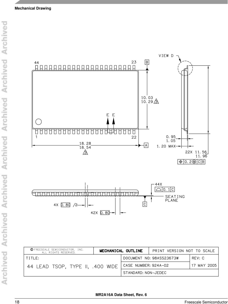
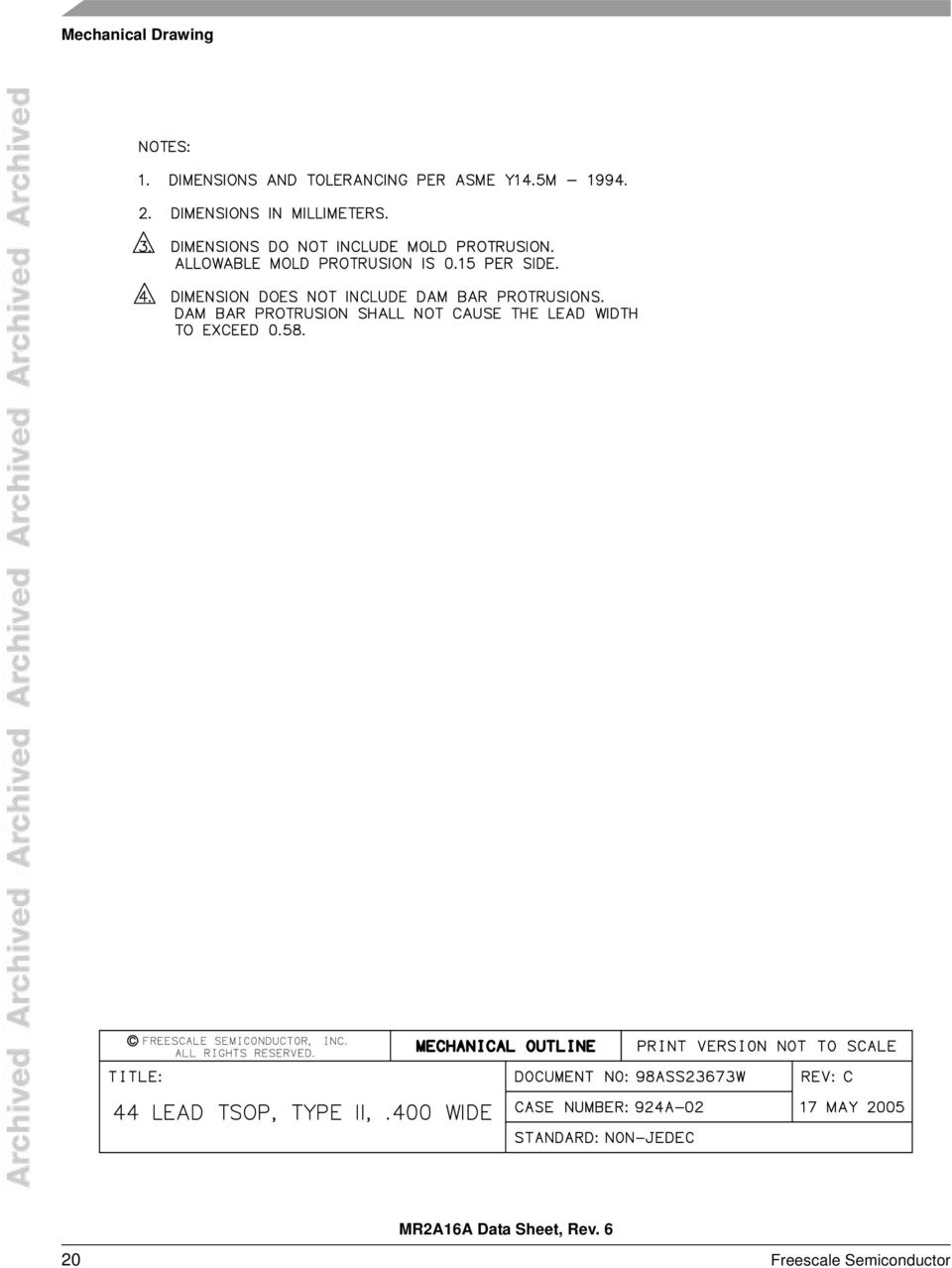
17 Package Information Package Information Table 13. Package Information Device Pin Count Package Type Designator Case No. Document No. RoHS Compliant MR2A16A 44 TSOP Type II TS/YS 1 924A-02 9ASS23673W True NOTES: 1 TS and YS are both valid package codes for TSOP packages. The package is identical for both TS and YS codes. Revision History Revision History Revision Date Description of Change 4 1 Jun Sep Nov 2007 Added new Industrial and Extended temperature product information; updated part ordering information; changed to 2 ms delay after power up; power supply characteristics values updated to TBD for industrial and extended temperature devices. Changed MR2A16ATS35C product description to Legacy Commercial. Added the New Commercial temperature product (MR2A16AYS35) information. Table 3: MR2A16AYS35 H max_write = 25 Oe. Table 4: MR2A16AYS35 has a 2 ms power up waiting period. Table 6: Applied values to TBD s in IDD specifications. Table 2: Changed IDDA to IDDR or IDDW. Table 13: Added note indicating that TS and YS are both valid package codes. Current Part Numbering System: Added commercial (missing letter) temperature range. Mechanical Drawing The following pages detail the package available to MR2A16A. Freescale Semiconductor 17

18 Mechanical Drawing 1 Freescale Semiconductor
19 Mechanical Drawing Freescale Semiconductor 19

20 Mechanical Drawing 20 Freescale Semiconductor
21 Mechanical Drawing Freescale Semiconductor 21
22 How to Reach Us: USA/Europe/Locations not listed: Freescale Semiconductor Literature Distribution P.O. Box 5405, Denver, Colorado or Japan: Freescale Semiconductor Japan Ltd. SPS, Technical Information Center , Minami-Azabu Minato-ku Tokyo , Japan Asia/Pacific: Freescale Semiconductor H.K. Ltd. 2 Dai King Street Tai Po Industrial Estate Tai Po, N.T. Hong Kong Learn More: For more information about Freescale Semiconductor products, please visit Information in this document is provided solely to enable system and software implementers to use Freescale Semiconductor products. There are no express or implied copyright licenses granted hereunder to design or fabricate any integrated circuits or integrated circuits based on the information in this document. Freescale Semiconductor reserves the right to make changes without further notice to any products herein. Freescale Semiconductor makes no warranty, representation or guarantee regarding the suitability of its products for any particular purpose, nor does Freescale Semiconductor assume any liability arising out of the application or use of any product or circuit, and specifically disclaims any and all liability, including without limitation consequential or incidental damages. Typical parameters which may be provided in Freescale Semiconductor data sheets and/or specifications can and do vary in different applications and actual performance may vary over time. All operating parameters, including Typicals must be validated for each customer application by customer s technical experts. Freescale Semiconductor does not convey any license under its patent rights nor the rights of others. Freescale Semiconductor products are not designed, intended, or authorized for use as components in systems intended for surgical implant into the body, or other applications intended to support or sustain life, or for any other application in which the failure of the Freescale Semiconductor product could create a situation where personal injury or death may occur. Should Buyer purchase or use Freescale Semiconductor products for any such unintended or unauthorized application, Buyer shall indemnify and hold Freescale Semiconductor and its officers, employees, subsidiaries, affiliates, and distributors harmless against all claims, costs, damages, and expenses, and reasonable attorney fees arising out of, directly or indirectly, any claim of personal injury or death associated with such unintended or unauthorized use, even if such claim alleges that Freescale Semiconductor was negligent regarding the design or manufacture of the part. Freescale and the Freescale logo are trademarks of Freescale Semiconductor, Inc. All other product or service names are the property of their respective owners. Freescale Semiconductor, Inc. 2004, 2005, 2006, MR2A16A Rev. 6, 11/2007
MR25H10. RoHS FEATURES INTRODUCTION
 FEATURES No write delays Unlimited write endurance Data retention greater than 20 years Automatic data protection on power loss Block write protection Fast, simple SPI interface with up to 40 MHz clock
MC14008B. 4-Bit Full Adder
 4-Bit Full Adder The MC4008B 4bit full adder is constructed with MOS PChannel and NChannel enhancement mode devices in a single monolithic structure. This device consists of four full adders with fast
SEMICONDUCTOR TECHNICAL DATA
 SEMICONDUCTOR TECHNICAL DATA Order this document by MPX5050/D The MPX5050 series piezoresistive transducer is a state of the art monolithic silicon pressure sensor designed for a wide range of applications,
SEMICONDUCTOR TECHNICAL DATA
 SEMICONDUCTOR TECHNICAL DATA The B Series logic gates are constructed with P and N channel enhancement mode devices in a single monolithic structure (Complementary MOS). Their primary use is where low
Local Interconnect Network (LIN) Physical Interface
 Physical Interface") Freescale Semiconductor Engineering Bulletin EB215 Rev. 1.0, 03/2005 Local Interconnect Network (LIN) Physical Interface Difference Between MC33399 and MC33661 Introduction This engineering bulletin highlights
Freescale Semiconductor Engineering Bulletin EB215 Rev. 1.0, 03/2005 Local Interconnect Network (LIN) Physical Interface Difference Between MC33399 and MC33661 Introduction This engineering bulletin highlights
LOW POWER SCHOTTKY. http://onsemi.com GUARANTEED OPERATING RANGES ORDERING INFORMATION
 The TTL/MSI SN74LS151 is a high speed 8-input Digital Multiplexer. It provides, in one package, the ability to select one bit of data from up to eight sources. The LS151 can be used as a universal function
DG2302. High-Speed, Low r ON, SPST Analog Switch. Vishay Siliconix. (1-Bit Bus Switch with Level-Shifter) RoHS* COMPLIANT DESCRIPTION FEATURES
 RoHS* COMPLIANT DESCRIPTION FEATURES") High-Speed, Low r ON, SPST Analog Switch (1-Bit Bus Switch with Level-Shifter) DG2302 DESCRIPTION The DG2302 is a high-speed, 1-bit, low power, TTLcompatible bus switch. Using sub-micron CMOS technology,
High-Speed, Low r ON, SPST Analog Switch (1-Bit Bus Switch with Level-Shifter) DG2302 DESCRIPTION The DG2302 is a high-speed, 1-bit, low power, TTLcompatible bus switch. Using sub-micron CMOS technology,
ULN2803A ULN2804A OCTAL PERIPHERAL DRIVER ARRAYS
 Order this document by ULN283/D The eight NPN Darlington connected transistors in this family of arrays are ideally suited for interfacing between low logic level digital circuitry (such as TTL, CMOS or
High-Speed, Low r ON, SPST Analog Switch (1-Bit Bus Switch)
") High-Speed, Low r ON, SPST Analog Switch (1-Bit Bus Switch) DG2301 ishay Siliconix DESCRIPTION The DG2301 is a high-speed, 1-bit, low power, TTLcompatible bus switch. Using sub-micron CMOS technology,
High-Speed, Low r ON, SPST Analog Switch (1-Bit Bus Switch) DG2301 ishay Siliconix DESCRIPTION The DG2301 is a high-speed, 1-bit, low power, TTLcompatible bus switch. Using sub-micron CMOS technology,
etpu Host Interface by:
 Freescale Semiconductor Application Note AN2821 Rev. 2, 08/2007 etpu Host Interface by: David Paterson Ming Li MCD Applications 1 Introduction This application note discusses the enhanced Time Processing
PQ-MDS-T1 Module. HW Getting Started Guide. Contents. About This Document. Required Reading. Definitions, Acronyms, and Abbreviations
 HW Getting Started Guide PQ-MDS-T1 Module April 2006: Rev. 0.3 Contents Contents................................................................................. 1 About This Document.......................................................................
DS1220Y 16k Nonvolatile SRAM
 19-5579; Rev 10/10 NOT RECOENDED FOR NEW DESIGNS 16k Nonvolatile SRAM www.maxim-ic.com FEATURES 10 years minimum data retention in the absence of external power Data is automatically protected during power
LC898300XA. Functions Automatic adjustment to the individual resonance frequency Automatic brake function Initial drive frequency adjustment function
 Ordering number : A2053 CMOS LSI Linear Vibrator Driver IC http://onsemi.com Overview is a Linear Vibrator Driver IC for a haptics and a vibrator installed in mobile equipments. The best feature is it
P D 215 1.25 Operating Junction Temperature T J 200 C Storage Temperature Range T stg 65 to +150 C
 SEMICONDUCTOR TECHNICAL DATA Order this document by /D The RF Line The is designed for output stages in band IV and V TV transmitter amplifiers. It incorporates high value emitter ballast resistors, gold
NTMS4920NR2G. Power MOSFET 30 V, 17 A, N Channel, SO 8 Features
 NTMS9N Power MOSFET 3 V, 7 A, N Channel, SO Features Low R DS(on) to Minimize Conduction Losses Low Capacitance to Minimize Driver Losses Optimized Gate Charge to Minimize Switching Losses These Devices
CAT28C64B F R E E. 64K-Bit CMOS PARALLEL EEPROM L E A D FEATURES DESCRIPTION BLOCK DIAGRAM
 64K-Bit CMOS PARALLEL EEPROM FEATURES Fast read access times: 90/120/150ns Low power CMOS dissipation: Active: 25 ma max. Standby: 100 µa max. Simple write operation: On-chip address and data latches Self-timed
MC10SX1190. Fibre Channel Coaxial Cable Driver and Loop Resiliency Circuit
 Fibre Channel Coaxial Cable Driver and Loop Resiliency Circuit Description The MC10SX1190 is a differential receiver, differential transmitter specifically designed to drive coaxial cables. It incorporates
Programming Audio Applications in the i.mx21 MC9328MX21
 Freescale Semiconductor Application Note Document Number: AN2628 Rev. 1, 10/2005 Programming Audio Applications in the MC9328MX21 by: Alfred Sin 1 Abstract The MC9328MX21 () processor has two dedicated
HEF4011B. 1. General description. 2. Features and benefits. 3. Ordering information. 4. Functional diagram. Quad 2-input NAND gate
 Rev. 6 10 December 2015 Product data sheet 1. General description 2. Features and benefits 3. Ordering information The is a quad 2-input NAND gate. The outputs are fully buffered for the highest noise
1-Mbit (128K x 8) Static RAM
 Static RAM") 1-Mbit (128K x 8) Static RAM Features Pin- and function-compatible with CY7C109B/CY7C1009B High speed t AA = 10 ns Low active power I CC = 80 ma @ 10 ns Low CMOS standby power I SB2 = 3 ma 2.0V Data Retention
1-Mbit (128K x 8) Static RAM Features Pin- and function-compatible with CY7C109B/CY7C1009B High speed t AA = 10 ns Low active power I CC = 80 ma @ 10 ns Low CMOS standby power I SB2 = 3 ma 2.0V Data Retention
256K (32K x 8) Static RAM
 Static RAM") 256K (32K x 8) Static RAM Features High speed: 55 ns and 70 ns Voltage range: 4.5V 5.5V operation Low active power (70 ns, LL version) 275 mw (max.) Low standby power (70 ns, LL version) 28 µw (max.) Easy
256K (32K x 8) Static RAM Features High speed: 55 ns and 70 ns Voltage range: 4.5V 5.5V operation Low active power (70 ns, LL version) 275 mw (max.) Low standby power (70 ns, LL version) 28 µw (max.) Easy
MC14001B Series. B Suffix Series CMOS Gates MC14001B, MC14011B, MC14023B, MC14025B, MC14071B, MC14073B, MC14081B, MC14082B
 MC4B Series BSuffix Series CMOS Gates MC4B, MC4B, MC4B, MC4B, MC4B, MC4B, MC4B, MC4B The B Series logic gates are constructed with P and N channel enhancement mode devices in a single monolithic structure
LOW POWER SCHOTTKY. http://onsemi.com GUARANTEED OPERATING RANGES ORDERING INFORMATION PLASTIC N SUFFIX CASE 648 SOIC D SUFFIX CASE 751B
 The SN74LS47 are Low Power Schottky BCD to 7-Segment Decoder/ Drivers consisting of NAND gates, input buffers and seven AND-OR-INVERT gates. They offer active LOW, high sink current outputs for driving
Features. Instruction. Decoder Control Logic, And Clock Generators. Address Compare amd Write Enable. Protect Register V PP.
 February 1999 NM9366 (MICROWIRE Bus Interface) 4096-Bit Serial EEPROM General Description The NM9366 devices are 4096 bits of CMOS non-volatile electrically erasable memory divided into 256 16-bit registers.
INTEGRATED CIRCUITS. 74LVC08A Quad 2-input AND gate. Product specification IC24 Data Handbook. 1997 Jun 30
 INTEGRATED CIRCUITS IC24 Data Handbook 1997 Jun 30 FEATURES Wide supply voltage range of 1.2 V to 3.6 V In accordance with JEDEC standard no. 8-1A Inputs accept voltages up to 5.5 V CMOS low power consumption
DS1220Y 16k Nonvolatile SRAM
 Not Recommended for New Design DS122Y 16k Nonvolatile SRAM www.maxim-ic.com FEATURES years minimum data retention in the absence of external power Data is automatically protected during power loss Directly
LOW POWER NARROWBAND FM IF
 Order this document by MC336B/D The MC336B includes an Oscillator, Mixer, Limiting Amplifier, Quadrature Discriminator, Active Filter, Squelch, Scan Control and Mute Switch. This device is designed for
AND8336. Design Examples of On Board Dual Supply Voltage Logic Translators. Prepared by: Jim Lepkowski ON Semiconductor. http://onsemi.
 Design Examples of On Board Dual Supply Voltage Logic Translators Prepared by: Jim Lepkowski ON Semiconductor Introduction Logic translators can be used to connect ICs together that are located on the
HEF4021B. 1. General description. 2. Features and benefits. 3. Ordering information. 8-bit static shift register
 Rev. 10 21 March 2016 Product data sheet 1. General description 2. Features and benefits 3. Ordering information The is an (parallel-to-serial converter) with a synchronous serial data input (DS), a clock
1-of-4 decoder/demultiplexer
 Rev. 6 1 April 2016 Product data sheet 1. General description 2. Features and benefits 3. Applications The contains two 1-of-4 decoders/demultiplexers. Each has two address inputs (na0 and na1, an active
MPC8245/MPC8241 Memory Clock Design Guidelines: Part 1
 Freescale Semiconductor AN2164 Rev. 4.1, 03/2007 MPC8245/MPC8241 Memory Clock Design Guidelines: Part 1 by Esther C. Alexander RISC Applications, CPD Freescale Semiconductor, Inc. Austin, TX This application
MM74C150 MM82C19 16-Line to 1-Line Multiplexer 3-STATE 16-Line to 1-Line Multiplexer
 MM74C150 MM82C19 16-Line to 1-Line Multiplexer 3-STATE 16-Line to 1-Line Multiplexer General Description The MM74C150 and MM82C19 multiplex 16 digital lines to 1 output. A 4-bit address code determines
3-to-8 line decoder, demultiplexer with address latches
 Rev. 7 29 January 2016 Product data sheet 1. General description The is a high-speed Si-gate CMOS device and is pin compatible with low-power Schottky TTL (LSTTL). The is specified in compliance with JEDEC
ESD7484. 4-Line Ultra-Large Bandwidth ESD Protection
 4-Line Ultra-Large Bandwidth ESD Protection Functional Description The ESD7484 chip is a monolithic, application specific discrete device dedicated to ESD protection of the HDMI connection. It also offers
Understanding LCD Memory and Bus Bandwidth Requirements ColdFire, LCD, and Crossbar Switch
 Freescale Semiconductor Application Note Document Number: AN3606 Rev. 0, 03/2008 Understanding LCD Memory and Bus Bandwidth Requirements ColdFire, LCD, and Crossbar Switch by: Melissa Hunter TSPG Applications
CD4043BC CD4044BC Quad 3-STATE NOR R/S Latches Quad 3-STATE NAND R/S Latches
 CD4043BC CD4044BC Quad 3-STATE NOR R/S Latches Quad 3-STATE NAND R/S Latches General Description The CD4043BC are quad cross-couple 3-STATE CMOS NOR latches, and the CD4044BC are quad cross-couple 3- STATE
NOTE: The Flatpak version has the same pinouts (Connection Diagram) as the Dual In-Line Package.
 as the Dual In-Line Package.") PRESETTABLE BCD/DECADE UP/DOWN COUNTERS PRESETTABLE 4-BIT BINARY UP/DOWN COUNTERS The SN54/74LS190 is a synchronous UP/DOWN BCD Decade (8421) Counter and the SN54/74LS191 is a synchronous UP/DOWN Modulo-
PRESETTABLE BCD/DECADE UP/DOWN COUNTERS PRESETTABLE 4-BIT BINARY UP/DOWN COUNTERS The SN54/74LS190 is a synchronous UP/DOWN BCD Decade (8421) Counter and the SN54/74LS191 is a synchronous UP/DOWN Modulo-
Features INSTRUCTION DECODER CONTROL LOGIC AND CLOCK GENERATORS COMPARATOR AND WRITE ENABLE EEPROM ARRAY READ/WRITE AMPS 16
 July 2000 FM9346 (MICROWIRE Bus Interface) 1024- Serial EEPROM General Description FM9346 is a 1024-bit CMOS non-volatile EEPROM organized as 64 x 16-bit array. This device features MICROWIRE interface
MC33064DM 5 UNDERVOLTAGE SENSING CIRCUIT
 Order this document by MC3464/D The MC3464 is an undervoltage sensing circuit specifically designed for use as a reset controller in microprocessor-based systems. It offers the designer an economical solution
MC14175B/D. Quad Type D Flip-Flop
 Quad Type D Flip-Flop The MC475B quad type D flipflop is cotructed with MOS Pchannel and Nchannel enhancement mode devices in a single monolithic structure. Each of the four flipflops is positiveedge triggered
DS1225Y 64k Nonvolatile SRAM
 DS1225Y 64k Nonvolatile SRAM www.maxim-ic.com FEATURES years minimum data retention in the absence of external power Data is automatically protected during power loss Directly replaces 2k x 8 volatile
Genesi Pegasos II Setup
 Freescale Semiconductor Application Note AN2666 Rev. 0, 07/2004 Genesi Pegasos II Setup by Maurie Ommerman CPD Applications Freescale Semiconductor, Inc. Austin, TX This application note is the first in
Handling Freescale Pressure Sensors
 Freescale Semiconductor Application Note Rev 3, 11/2006 Handling Freescale Pressure by: William McDonald INTRODUCTION Smaller package outlines and higher board densities require the need for automated
User Guide. Introduction. HCS12PLLCALUG/D Rev. 0, 12/2002. HCS12 PLL Component Calculator
 User Guide HCS12PLLCALUG/D Rev. 0, 12/2002 HCS12 PLL Component Calculator by Stuart Robb Applications Engineering Motorola, East Kilbride Introduction The MC9S12D amily o MCUs includes a Phase-Locked Loop
LC03-6R2G. Low Capacitance Surface Mount TVS for High-Speed Data Interfaces. SO-8 LOW CAPACITANCE VOLTAGE SUPPRESSOR 2 kw PEAK POWER 6 VOLTS
 Low Capacitance Surface Mount TVS for High-Speed Data terfaces The LC3- transient voltage suppressor is designed to protect equipment attached to high speed communication lines from ESD, EFT, and lighting.
Quad 2-input NAND Schmitt trigger
 Rev. 9 15 December 2015 Product data sheet 1. General description 2. Features and benefits 3. Applications The is a quad two-input NAND gate. Each input has a Schmitt trigger circuit. The gate switches
Freescale Semiconductor, Inc. Product Brief Integrated Portable System Processor DragonBall ΤΜ
 nc. Order this document by MC68328/D Microprocessor and Memory Technologies Group MC68328 MC68328V Product Brief Integrated Portable System Processor DragonBall ΤΜ As the portable consumer market grows
1 TO 4 CLOCK BUFFER ICS551. Description. Features. Block Diagram DATASHEET
 DATASHEET 1 TO 4 CLOCK BUFFER ICS551 Description The ICS551 is a low cost, high-speed single input to four output clock buffer. Part of IDT s ClockBlocks TM family, this is our lowest cost, small clock
MMBZ52xxBLT1G Series, SZMMBZ52xxBLT3G. Zener Voltage Regulators. 225 mw SOT 23 Surface Mount
 MMBZ5xxBLTG Series, SZMMBZ5xxBLTG Series Zener Voltage Regulators 5 mw SOT Surface Mount This series of Zener diodes is offered in the convenient, surface mount plastic SOT package. These devices are designed
2N6387, 2N6388. Plastic Medium-Power Silicon Transistors DARLINGTON NPN SILICON POWER TRANSISTORS 8 AND 10 AMPERES 65 WATTS, 60-80 VOLTS
 2N6388 is a Preferred Device Plastic MediumPower Silicon Transistors These devices are designed for generalpurpose amplifier and lowspeed switching applications. Features High DC Current Gain h FE = 2500
2N3906. General Purpose Transistors. PNP Silicon. Pb Free Packages are Available* http://onsemi.com. Features MAXIMUM RATINGS
 2N396 General Purpose Transistors PNP Silicon Features PbFree Packages are Available* COLLECTOR 3 MAXIMUM RATINGS Rating Symbol Value Unit Collector Emitter Voltage V CEO 4 Vdc Collector Base Voltage V
MM74C150 MM82C19 16-Line to 1-Line Multiplexer 3-STATE 16-Line to 1-Line Multiplexer
 MM74C150 MM82C19 16-Line to 1-Line Multiplexer 3-STATE 16-Line to 1-Line Multiplexer General Description The MM74C150 and MM82C19 multiplex 16 digital lines to 1 output. A 4-bit address code determines
Blood Pressure Monitor Using Flexis QE128 Gabriel Sanchez RTAC Americas
 Freescale Semiconductor Application Note Document Number: AN3500 Rev. 0, 08/2007 Blood Pressure Monitor Using Flexis QE128 by: Gabriel Sanchez RTAC Americas 1 Introduction Product designers and developers
14-stage ripple-carry binary counter/divider and oscillator
 Rev. 8 25 March 2016 Product data sheet 1. General description 2. Features and benefits 3. Ordering information The is a with three oscillator terminals (RS, REXT and CEXT), ten buffered outputs (Q3 to
The 74LVC1G11 provides a single 3-input AND gate.
 Rev. 8 17 September 2015 Product data sheet 1. General description The provides a single 3-input AND gate. The input can be driven from either 3.3 V or 5 V devices. This feature allows the use of this
Spread Spectrum Clock Generator
 Spread Spectrum Clock Generator Features Generates a 1x (PCS3P5811), x (PCS3P581) and 4x() low EMI spread spectrum clock of the input frequency Provides up to 15dB of EMI suppression Input Frequency: 4MHz
MM54C150 MM74C150 16-Line to 1-Line Multiplexer
 MM54C150 MM74C150 16-Line to 1-Line Multiplexer MM72C19 MM82C19 TRI-STATE 16-Line to 1-Line Multiplexer General Description The MM54C150 MM74C150 and MM72C19 MM82C19 multiplex 16 digital lines to 1 output
HEF4013B. 1. General description. 2. Features and benefits. 3. Applications. 4. Ordering information. Dual D-type flip-flop
 Rev. 9 10 December 2015 Product data sheet 1. General description 2. Features and benefits 3. Applications The is a dual D-type flip-flop that features independent set-direct input (SD), clear-direct input
3-input EXCLUSIVE-OR gate. The 74LVC1G386 provides a 3-input EXCLUSIVE-OR function.
 Rev. 02 3 September 2007 Product data sheet 1. General description The provides a 3-input EXCLUSIVE-OR function. The input can be driven from either 3.3 or 5 V devices. This feature allows the use of these
74HC595; 74HCT595. 1. General description. 2. Features and benefits. 3. Applications
 8-bit serial-in, serial or parallel-out shift register with output latches; 3-state Rev. 7 26 January 2015 Product data sheet 1. General description The are high-speed Si-gate CMOS devices and are pin
HCF4056B BCD TO 7 SEGMENT DECODER /DRIVER WITH STROBED LATCH FUNCTION
 BCD TO 7 SEGMENT DECODER /DRIVER WITH STROBED LATCH FUNCTION QUIESCENT CURRENT SPECIF. UP TO 20V OPERATION OF LIQUID CRYSTALS WITH CMOS CIRCUITS PROVIDES ULTRA LOW POWER DISPLAY. EQUIVALENT AC OUTPUT DRIVE
4-Mbit (256K x 16) Static RAM
 Static RAM") 4-Mbit (256K x 16) Static RAM Features Pin- and function-compatible with CY7C1041CV33 High speed t AA =10 ns Low active power I CC = 90 ma @ 10 ns (Industrial) Low CMOS standby power I SB2 = 10 ma 2.0
4-Mbit (256K x 16) Static RAM Features Pin- and function-compatible with CY7C1041CV33 High speed t AA =10 ns Low active power I CC = 90 ma @ 10 ns (Industrial) Low CMOS standby power I SB2 = 10 ma 2.0
Freescale Semiconductor. Integrated Silicon Pressure Sensor. On-Chip Signal Conditioned, Temperature Compensated and Calibrated MPX4080D.
 Freescale Semiconductor Integrated Silicon Pressure Sensor + On-Chip Signal Conditioned, Temperature Compensated and Calibrated The series piezoresistive transducer is a state-of-the-art monolithic silicon
2N3903, 2N3904. General Purpose Transistors. NPN Silicon. Pb Free Packages are Available* Features. http://onsemi.com MAXIMUM RATINGS
 N393, General Purpose Transistors NPN Silicon Features PbFree Packages are Available* MAXIMUM RATINGS Rating Symbol Value Unit CollectorEmitter Voltage V CEO 4 Vdc CollectorBase Voltage V CBO 6 Vdc EmitterBase
2N6056. NPN Darlington Silicon Power Transistor DARLINGTON 8 AMPERE SILICON POWER TRANSISTOR 80 VOLTS, 100 WATTS
 NPN Darlington Silicon Power Transistor The NPN Darlington silicon power transistor is designed for general purpose amplifier and low frequency switching applications. High DC Current Gain h FE = 3000
How To Fit A 2Mm Exposed Pad To A Dfn Package
 EVERSPIN s New 2mm Exposed Pad DFN Package Meets Both SOIC-8 and DFN8 PCB Layouts This Application Note is to inform Everspin customers that a new, DFN8 package with a 2mm bottom exposed pad has been added
SN54/74LS240 SN54/74LS241 SN54/74LS244 OCTAL BUFFER/LINE DRIVER WITH 3-STATE OUTPUTS OCTAL BUFFER/ LINE DRIVER WITH 3-STATE OUTPUTS
 OCTA BUFFER/INE RIVER WIT 3-STATE S The SN54/S240, 241 and 244 are Octal Buffers and ine rivers designed to be employed as memory address drivers, clock drivers and bus-oriented transmitters/receivers
INTEGRATED CIRCUITS. 74F153 Dual 4-line to 1-line multiplexer. Product specification 1996 Jan 05 IC15 Data Handbook
 INTEGRATED CIRCUITS 1996 Jan 05 IC15 Data Handbook FEATURES Non-inverting outputs Separate enable for each section Common select inputs See 74F253 for 3-State version PIN CONFIGURATION Ea 1 S1 2 I3a 3
Initializing the TSEC Controller
 Freescale Semiconductor Application Note Document Number: AN2925 Rev. 0, 11/2005 Initializing the TSEC Controller by Ahsan Kabir Digital Systems Division Freescale Semiconductor, Inc. Austin, TX This application
SN54/74LS682 SN54/74LS684 8-BIT MAGNITUDE COMPARATORS SN54/74LS688 8-BIT MAGNITUDE COMPARATORS FAST AND LS TTL DATA 5-603
 8-BIT MAGNITUDE COMPARATORS The SN54/ 74LS682, 684, 688 are 8-bit magnitude comparators. These device types are designed to perform compariso between two eight-bit binary or BCD words. All device types
LB1836M. Specifications. Monolithic Digital IC Low-Saturation Bidirectional Motor Driver for Low-Voltage Drive. Absolute Maximum Ratings at Ta = 25 C
 Ordering number : EN397F LB136M Monolithic Digital IC Low-Saturation Bidirectional Motor Driver for Low-Voltage Drive http://onsemi.com Overview The LB136M is a low-saturation two-channel bidirectional
2N5460, 2N5461, 2N5462. JFET Amplifier. P Channel Depletion. Pb Free Packages are Available* Features. http://onsemi.com MAXIMUM RATINGS
 2N546, 2N5461, JFET Amplifier PChannel Depletion Features PbFree Packages are Available* MAXIMUM RATINGS Rating Symbol Value Unit Drain Gate Voltage V DG 4 Vdc Reverse Gate Source Voltage V GSR 4 Vdc Forward
256K (32K x 8) OTP EPROM AT27C256R 256K EPROM. Features. Description. Pin Configurations
 OTP EPROM AT27C256R 256K EPROM. Features. Description. Pin Configurations") Features Fast Read Access Time - 45 ns Low-Power CMOS Operation 100 µa max. Standby 20 ma max. Active at 5 MHz JEDEC Standard Packages 28-Lead 600-mil PDIP 32-Lead PLCC 28-Lead TSOP and SOIC 5V ± 10% Supply
Features Fast Read Access Time - 45 ns Low-Power CMOS Operation 100 µa max. Standby 20 ma max. Active at 5 MHz JEDEC Standard Packages 28-Lead 600-mil PDIP 32-Lead PLCC 28-Lead TSOP and SOIC 5V ± 10% Supply
Vdc. Vdc. Adc. W W/ C T J, T stg 65 to + 200 C
 2N6284 (NPN); 2N6286, Preferred Device Darlington Complementary Silicon Power Transistors These packages are designed for general purpose amplifier and low frequency switching applications. Features High
Freescale Semiconductor. Integrated Silicon Pressure Sensor. On-Chip Signal Conditioned, Temperature Compensated and Calibrated MPX5500.
 Freescale Semiconductor Integrated Silicon Pressure Sensor + On-Chip Signal Conditioned, Temperature Compensated and Calibrated Series Pressure Rev 7, 09/2009 0 to 500 kpa (0 to 72.5 psi) 0.2 to 4.7 V
IDT6116SA IDT6116LA. CMOS Static RAM 16K (2K x 8-Bit)
") CMOS Static RAM 16K (2K x 8-Bit) IDT6116SA IDT6116LA Features High-speed access and chip select times Military: 2/2/3/4//7/9/12/1 (max.) Industrial: 2/2/3/4 (max.) Commercial: 1/2/2/3/4 (max.) Low-power
CMOS Static RAM 16K (2K x 8-Bit) IDT6116SA IDT6116LA Features High-speed access and chip select times Military: 2/2/3/4//7/9/12/1 (max.) Industrial: 2/2/3/4 (max.) Commercial: 1/2/2/3/4 (max.) Low-power
www.jameco.com 1-800-831-4242
 Distributed by: www.jameco.com 1-800-831-4242 The content and copyrights of the attached material are the property of its owner. www.maxim-ic.com FEATURES 10 years minimum data retention in the absence
ESD9X3.3ST5G Series, SZESD9X3.3ST5G Series. Transient Voltage Suppressors Micro Packaged Diodes for ESD Protection
 ESD9X3.3ST5G Series, SZESD9X3.3ST5G Series Transient Voltage Suppressors Micro Packaged Diodes for ESD Protection The ESD9X Series is designed to protect voltage sensitive components from ESD. Excellent
MMSZxxxT1G Series, SZMMSZxxxT1G Series. Zener Voltage Regulators. 500 mw SOD 123 Surface Mount
 MMSZxxxTG Series, SZMMSZxxxTG Series Zener Voltage Regulators 5 mw SOD 3 Surface Mount Three complete series of Zener diodes are offered in the convenient, surface mount plastic SOD 3 package. These devices
2N4401. General Purpose Transistors. NPN Silicon. Pb Free Packages are Available* http://onsemi.com. Features MAXIMUM RATINGS THERMAL CHARACTERISTICS
 General Purpose Transistors NPN Silicon Features PbFree Packages are Available* MAXIMUM RATINGS Rating Symbol Value Unit Collector Emitter Voltage V CEO 4 Vdc Collector Base Voltage V CBO 6 Vdc Emitter
Hardware Configurations for the i.mx Family USB Modules
 Freescale Semiconductor Application Note Document Number: AN4136 Rev. 0, 06/2010 Hardware Configurations for the i.mx Family USB Modules by Multimedia Applications Division Freescale Semiconductor, Inc.
PowerQUICC II Pro (MPC83xx) PCI Agent Initialization
 PCI Agent Initialization") Freescale Semiconductor Application Note Document Number: AN3373 Rev. 0, 04/2007 PowerQUICC II Pro (MPC83xx) PCI Agent Initialization by: David Smith Field Application Engineering Raleigh, NC In many designs,
Freescale Semiconductor Application Note Document Number: AN3373 Rev. 0, 04/2007 PowerQUICC II Pro (MPC83xx) PCI Agent Initialization by: David Smith Field Application Engineering Raleigh, NC In many designs,
74F257A Quad 2-line to 1-line selector/multiplexer, non-inverting (3-State)
") INTEGRATED CIRCUITS Quad 2-line to 1-line selector/multiplexer, non-inverting (3-State) 1995 Mar 31 IC15 Data Handbook Philips Semiconductors Quad 2-line to 1-line selector/multiplexer, non-inverting (3-State)
INTEGRATED CIRCUITS Quad 2-line to 1-line selector/multiplexer, non-inverting (3-State) 1995 Mar 31 IC15 Data Handbook Philips Semiconductors Quad 2-line to 1-line selector/multiplexer, non-inverting (3-State)
MM74HCT373 MM74HCT374 3-STATE Octal D-Type Latch 3-STATE Octal D-Type Flip-Flop
 3-STATE Octal D-Type Latch 3-STATE Octal D-Type Flip-Flop General Description The MM74HCT373 octal D-type latches and MM74HCT374 Octal D-type flip flops advanced silicongate CMOS technology, which provides
Triple single-pole double-throw analog switch
 Rev. 12 25 March 2016 Product data sheet 1. General description 2. Features and benefits 3. Applications 4. Ordering information The is a triple single-pole double-throw (SPDT) analog switch, suitable
MMBF4391LT1G, SMMBF4391LT1G, MMBF4392LT1G, MMBF4393LT1G. JFET Switching Transistors. N Channel
 LT1G, SLT1G, LT1G, LT1G JFET Switching Transistors NChannel Features S Prefix for Automotive and Other Applications Requiring Unique Site and Control Change Requirements; AECQ1 Qualified and PPAP Capable
MCF54418 NAND Flash Controller
 Freescale Semiconductor Application Note Document Number: AN4348 Rev. 0, 09/2011 MCF54418 NAND Flash Controller by: Liew Tsi Chung Applications Engineer 1 Introduction The ColdFire MCF5441x family is the
HCF4081B QUAD 2 INPUT AND GATE
 QUAD 2 INPUT AND GATE MEDIUM SPEED OPERATION : t PD = 60ns (Typ.) at 10 QUIESCENT CURRENT SPECIFIED UP TO 20 5, 10 AND 15 PARAMETRIC RATINGS INPUT LEAKAGE CURRENT I I = 100nA (MAX) AT DD = 18 T A = 25
CD4001BC/CD4011BC Quad 2-Input NOR Buffered B Series Gate Quad 2-Input NAND Buffered B Series Gate
 CD4001BC/CD4011BC Quad 2-Input NOR Buffered B Series Gate Quad 2-Input NAND Buffered B Series Gate General Description The CD4001BC and CD4011BC quad gates are monolithic complementary MOS (CMOS) integrated
NLSX4378. 4-Bit 24 Mb/s Dual-Supply Level Translator
 4-Bit 24 Mb/s Dual-Supply Level Translator The NLSX4378 is a 4 bit configurable dual supply bidirectional auto sensing translator that does not require a directional control pin. The I/O and I/O ports
LM350. 3.0 A, Adjustable Output, Positive Voltage Regulator THREE TERMINAL ADJUSTABLE POSITIVE VOLTAGE REGULATOR
 3. A, able Output, Positive Voltage Regulator The is an adjustable threeterminal positive voltage regulator capable of supplying in excess of 3. A over an output voltage range of 1.2 V to 33 V. This voltage
MM74HC273 Octal D-Type Flip-Flops with Clear
 MM74HC273 Octal D-Type Flip-Flops with Clear General Description The MM74HC273 edge triggered flip-flops utilize advanced silicon-gate CMOS technology to implement D-type flipflops. They possess high noise
4-Mbit (256K x 16) Static RAM
 Static RAM") 4-Mbit (256K x 16) Static RAM Features Pin equivalent to CY7C1041BV33 Temperature Ranges Commercial: 0 C to 70 C Industrial: 40 C to 85 C Automotive: 40 C to 125 C High speed t AA = 10 ns Low active power
4-Mbit (256K x 16) Static RAM Features Pin equivalent to CY7C1041BV33 Temperature Ranges Commercial: 0 C to 70 C Industrial: 40 C to 85 C Automotive: 40 C to 125 C High speed t AA = 10 ns Low active power
74HC175; 74HCT175. Quad D-type flip-flop with reset; positive-edge trigger
 Rev. 5 29 January 2016 Product data sheet 1. General description 2. Features and benefits 3. Ordering information The is a quad positive-edge triggered D-type flip-flop with individual data inputs (Dn)
ULN2801A, ULN2802A, ULN2803A, ULN2804A
 ULN2801A, ULN2802A, ULN2803A, ULN2804A Eight Darlington array Datasheet production data Features Eight Darlington transistors with common emitters Output current to 500 ma Output voltage to 50 V Integral
Low-power configurable multiple function gate
 Rev. 7 10 September 2014 Product data sheet 1. General description The provides configurable multiple functions. The output state is determined by eight patterns of 3-bit input. The user can choose the
IRTC Compensation and 1 Hz Clock Generation
 Freescale Semiconductor Document Number: AN4257 Application Note Rev. 0, January 2011 IRTC Compensation and 1 Hz Clock Generation by: Derek Liu Applications Engineering Shanghai 1 Introduction The MC9S08GW64
HCF4070B QUAD EXCLUSIVE OR GATE
 QUAD EXCLUSIE OR GATE MEDIUM-SPEED OPERATION t PHL = t PLH = 70ns (Typ.) at CL = 50 pf and DD = 10 QUIESCENT CURRENT SPECIFIED UP TO 20 5, 10 AND 15 PARAMETRIC RATINGS INPUT LEAKAGE CURRENT I I = 100nA
V OUT. I o+ & I o- (typical) 2.3A & 3.3A. Package Type
 2.3A & 3.3A. Package Type") July 25 th, 2012 Automotive Grade AUIRS4427S DUAL LOW SIDE DRIVER Features Gate drive supply range from 6 V to 20 V CMOS Schmitt-triggered inputs 3.3V and 5V logic compatible Two independent gate drivers
July 25 th, 2012 Automotive Grade AUIRS4427S DUAL LOW SIDE DRIVER Features Gate drive supply range from 6 V to 20 V CMOS Schmitt-triggered inputs 3.3V and 5V logic compatible Two independent gate drivers
MM74HC14 Hex Inverting Schmitt Trigger
 MM74HC14 Hex Inverting Schmitt Trigger General Description The MM74HC14 utilizes advanced silicon-gate CMOS technology to achieve the low power dissipation and high noise immunity of standard CMOS, as