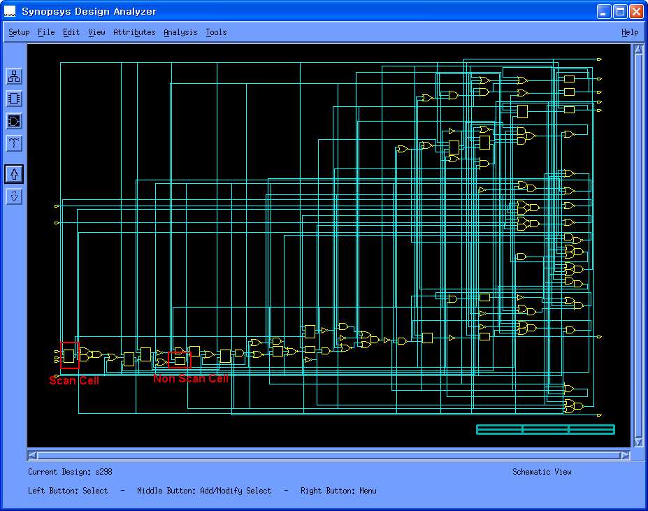
data D Q sc_in D Q data CLK sc_en CLK clk clk scan Flip Flop Nonscan Flip Flop - 1 -
|
|
|
- Hugo Wilkinson
- 7 years ago
- Views:
Transcription
1 data data D Q sc_in D Q clk CLK sc_en CLK clk Nonscan Flip Flop scan Flip Flop - 1 -
2 순차회로부 주사플립플롭 - 2 -
3 Partition A Design level Scan out pin added Design level Scan in pin added Unobservable Output Uncntrollable Input - 3 -
4 A B A B C D E F G H W1 W2 O C D T E F G H W2 W1 O a) Test point 가적용되지않은회로 b) controllability 를높이기위한 Test point 가적용된회로 T T A B TO A B TO C D E F W1 W2 O C D E F W1 O G H G H W2 c) observability 를높이기위한 Test point 가적용된회로 d) Test point 가적용된회로 - 4 -
5 test point (for observability) Combinational A Combinational B D si s e CLK Q so Next scan cell test point (for controllability) Combinational A Combinational B D si s e CLK Q so Next scan cell - 5 -

6 - 6 -

7 - 7 -
8 - 8 -

9 - 9 -
10 - 10 -

11 - 11 -

12 - 12 -

13 - 13 -
14 - 14 -
15 - 15 -
16 - 16 -

17 - 17 -
18 - 18 -
19 - 19 -
20 - 20 -
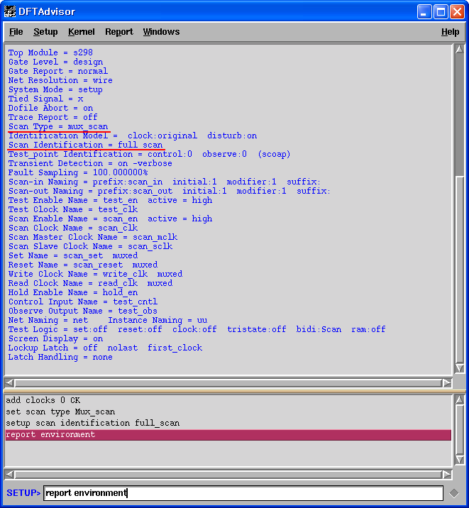
21 Add Black Box Add Black Box Add Cell Library Add Cell Models Add Clock Groups Add Clocks Add Display Instances Add Display Loop Add Display Path Add Display Scanpath Add Mapping Definition Add Nofaults Add Nonscan Instances Add Nonscan Models Add Notest Points Add Output Masks Add Pin Constraints Add Pin Equivalences Defines black boxes and sets the constrained value on output or bidirectional black box pins. Specifies for DFTAdvisor to place buffer cells between the primary input of the specified test pin and the gates that it drives. Specifies the EDIF library in which to place all or specified library models which are explicitly added by DFTAdvisor scan and test logic insertion process. Specifies the name of a DFT library cell that DFTAdvisor can use with user-defined test points, system-generated test points, and system-generated test logic. Specifies the grouping of scan cells controlled by different clocks onto one chain. Specifies the names and inactive states of the primary input pins that control the clocks in the design. Adds the specified instances to the netlist for display. Displays all the gates in a specified feedback path. Displays all the gates associated with the specified path. Displays all the associated gates between two positions in a scan chain. Overrides the nonscan to scan model mapping defined by DFTAdvisor. Places nofault settings either on a pin or on all pins of a specified instance or module. Specifies for DFTAdvisor to ignore the specified instances, all instances controlled by the specified control pin, or all instances within the specified module, when identifying and inserting the required scan elements and test logic. Instructs DFTAdvisor to ignore all instances of the specified sequential DFT library model when identifying and inserting the required scan elements and test logic into the design. Adds circuit points to list for exclusion from testability insertion. Instructs DFTAdvisor to mask, and optionally maintain a constant logic level on, the specified primary output pins during the scan identification analysis. Specifies that DFTAdvisor hold the input pin at a constant state during the rules checking and loop cutting processes. Specifies to hold the specified primary input pins at a state either equal to or inverted in relationship to the state of another primary input pin during rules checking
22 Add Primary Inputs Adds a primary input to the net. Add Primary Outputs Adds a primary output to the net. Adds an off-state value to specified RAM read control Add Read Controls lines. Specifies a name for a preexisting scan chain within the Add Scan Chains design. Add Scan Groups Adds one scan chain group to the system. Specifies that DFTAdvisor add the specified instance, all instances controlled by the specified control pin, or all Add Scan Instances instances within the specified module, to the scannable instance list. Specifies that DFTAdvisor is to flag every instance of the Add Scan Models named DFT library model for inclusion into the identified scan list. Declares the name of a scan chain at the top-level module and assigns the corresponding scan input pin, scan output Add Scan Pins pin, and optionally, the scan clock pin that you want to associate with that chain. Specifies the enable value of a clock enable that internally gates Add Seq_transparent Constraints the clock input of a non-scan cell for sequential transparent scan identification. Specifies the name of a preexisting scan chain that exists Add Sub Chains entirely within a module or instance within a hierarchical design. Specifies explicitly where DFTAdvisor is to place a Add Test Points user-defined test point to improve the design's testability either through better controllability or observability. Specifies for DFTAdvisor to hold the named floating Add Tied Signals objects (nets or pins) at the given state value. Specifies the off-state value of the write control lines for Add Write Controls RAMs. Identifies and optionally defines the primary inputs of Analyze Control Signals control signals. Generates a netlist of the portion of the design involved Analyze Drc Violation with the specified rule violation number. Specifies for DFTAdvisor to calculate and display the Analyze Input Control effects of constraining primary input pins to an unknown value on those pins' control capability. Specifies for DFTAdvisor to calculate and display the Analyze Output Observe effects on the observability of masked primary output pins. Reports general scannability and testability information, Analyze Testability along with calculating the controllability and observability values for gates. Terminates the optional schematic viewing application Close Schematic Viewer (DFTInsight)
23 Delete Black Box Delete Buffer Insertion Delete Cell Models Delete Clock Groups Delete Clocks Delete Display Instances Delete Mapping Definition Delete Nofaults Delete Nonscan Instances Delete Nonscan Models Delete Notest Points Delete Output Masks Delete Pin Constraints Delete Pin Equivalences Delete Primary Inputs Delete Primary Outputs Delete Read Controls Delete Scan Chains Delete Scan Groups Delete Scan Instances Delete Scan Models Delete Scan Pins Delete Seq_transparent Constraints Delete Sub Chains Delete Test Points Undoes the effect of the Add Black Box command. Specifies the type of scan test pins on which you want to remove the fanout limit. Specifies the name of the DFT library cell that DFTAdvisor is to remove from the active list of cells that the user can access when adding test points or that DFTAdvisor can access when inserting test logic. Specifies the name of the group that you want to remove from the clock groups list. Removes primary input pins from the clock list. Removes the specified objects from display in DFTInsight. Returns the nonscan to scan model mapping to the mapping defined by DFTAdvisor. Removes the no-fault settings from either the specified pin or instance pathnames. Removes the specified sequential instances from the non-scan instance list. Removes from the non-scan model list the specified sequential DFT library models. Removes the specified pins from the list of notest points which the tool cannot use for testability insertion. Removes the masking of the specified primary output pins. Removes the pin constraints from the specified primary input pins. Removes the pin equivalence specifications for the designated primary input pins. Removes the specified primary inputs from the current netlist. Removes the specified primary outputs from the current netlist. Removes the read control line off-state definitions from the specified primary input pins. Removes the specified scan chain definitions from the scan chain list. Removes the specified scan chain group definitions from the scan chain group list. Removes the specified, sequential instances from the user-identified scan instance list. Removes the specified sequential models from the scan model list. Removes any previously-assigned scan input, output, and clock names from the specified scan chains. Removes the pin constraints from the specified DFT library model input pins. Removes the definition of a preexisting scan sub-chain. Remove the test point definitions at the specified locations
24 Delete Tied Signals Delete Write Controls Dofile Exit Help H istory Insert Test Logic Load Core Access Load Core Description Mark Open Schematic Viewer Read Procfile Redo Display Report Black Box Report Buffer Insertion Report Cell Models Report Clock Groups Report Clocks Report Control Signals Report Dft Check Report Display Instances Report Drc Rules Report Environment Report Feedback Paths Report Flatten Rules Report Gates Report Loops Report Mapping Definition Report Nofaults Removes the assigned (tied) value from the specified floating nets or pins. Removes the RAM write control line off-state definitions from the specified primary input pins. Executes the commands contained within the specified file. Terminates the current DFTAdvisor session. Displays the usage syntax and system mode for the specified command. Displays a list of previously-executed commands. Inserts the test structures that you define into the netlist to increase the design's testability. Loads the specified core access file. Loads the specified core description file. Highlights the objects that you specify in the Schematic View window. Invokes the optional schematic viewing application, DFTInsight. Reads the specified enhanced procedure file. Nullifies the schematic view effects of an Undo command. Displays information on defined blackboxes. Displays a list of all the different scan test pins and the corresponding fanout limit. Displays a list of either all cell models or the DFT library models associated with the specified cell type. Displays a list of all clock group definitions. Displays a list of all clock definitions. Displays the rules checking results for the specified control signals. Generates the scannability check results for non-scan instances. Displays a textual report of the netlist information for either the gates or instances that you specify or for all the gates in the current schematic view display. Displays either a summary of all the Design Rule Check (DRC) violations or the data for a specific violation. Displays the current values of all the "set" commands and the default names of the scan type pins. Displays a textual report of the currently identified feedback paths. Displays either a summary of all the flattening rule violations or the data for a specific violation. Displays the netlist information for the specified gates. Displays a list of all the current loops. Reports the nonscan to scan model mapping defined in the design. Displays the no-fault settings for the specified pin or instance pathnames
25 Report Nonscan Instances Report Nonscan Models Report Notest Points Report Output Masks Report Pin Constraints Report Pin Equivalences Report Primary Inputs Report Primary Outputs Report Procedure Report Read Controls Report Scan Cells Report Scan Chains Report Scan Groups Report Scan Identification Report Scan Instances Report Scan Models Report Scan Pins Report Seq_transparent Constraints Report Statistics Report Sub Chains Report Test Logic Report Test Points Report Testability Analysis Report Tied Signals Report Timeplate Report Write Controls Reset State Ripup Scan Chains Displays the currently defined sequential non-scan instances. Displays the sequential non-scan model list. Displays all the circuit points for which you do not want DFTAdvisor to insert controllability and observability. Displays a list of the currently masked primary output pins. Displays the pin constraints of the primary inputs. Displays the pin equivalences of the primary inputs. Displays the specified primary inputs. Displays the specified primary outputs. Displays the specified procedure. Displays all of the currently defined read control lines. Displays a report or writes a file on the scan cells that reside in the specified scan chains. Displays a report on all the current scan chains. Displays a report on all the current scan chain groups. Displays a list of the scan instances which DFTAdvisor has identified or you have defined as scan cells. Displays the currently defined sequential scan instances. Displays the sequential scan models currently in the scan model list. Displays all previously assigned scan input, output, and clock names. Displays the seq_transparent constraints. Displays a detailed report of the design's statistics. Generates and displays a report on the scan sub-chains. Displays the test logic that DFTAdvisor added during the scan insertion process. Displays the test point specifications you created with Add Test Points command and any test points that you enabled DFTAdvisor to automatically identify. Displays the results of the Analyze Testability command. Displays a list of the tied floating signals and pins. Displays the specified timeplate. Displays the currently defined write control lines and their off-states. Removes all instances from both the scan identification and test point identification lists that DFTAdvisor identified during a run. Removes the specified scan chains from the design
26 Run Save History Save Schematic Select Object Set Capture Clock Set Command Editing Set Contention Check Set Control Threshold Set Dofile Abort Set Drc Handling Set Fault Sampling Set File Compression Set Flatten Handling Set Gate Level Set Gate Report Set Gzip Options Set Identification Model Set Instancename Visibility Set Internal Fault Set Io Insertion Set Latch Handling Set Lockup Latch Set Logfile Handling Set Loop Duplication Set Multiple Scan_enables Set Net Resolution Set Nonscan Handling Runs the scan or test point identification process. Saves the command line history file to the specified file. Saves the schematic currently displayed by DFTInsight. Selects the specified objects in the DFTInsight schematic view. Specifies the capture clock name for random pattern simulation. Sets the command line editing mode. Specifies whether DFTAdvisor checks the gate types that you determine for contention. Specifies the controllability value for simulation-based pseudorandom pattern test point identification. Lets you specify that the tool complete processing of all commands in a dofile regardless of an error detection. Specifies how DFTAdvisor globally handles design rule violations. Specifies the fault sampling percentage for scan identification. Controls whether the tools read and write files with.z or.gz extensions as compressed files (the default). Specifies how DFTAdvisor globally handles flattening violations. Specifies the hierarchical level of gate reporting and displaying. Specifies the additional display information for the Report Gates command. Specifies GNU gzip options to use with the GNU gzip command. Specifies the simulation model that DFTAdvisor uses to imitate the scan operation during the scan identification process. Specifies whether DFTInsight displays instance names immediately above each instance in the Schematic View area. Specifies whether the tool allows faults within or on the boundary of library models. Specifies whether to insert I/O buffers. Specifies whether the tool considers non-transparent latches for scan insertion while test logic is turned on. Specifies for DFTAdvisor to insert latches between different clock domains to synchronize the clocks within a scan chain. Specifies for DFTAdvisor to direct the transcript information to a file. Specifies whether to include duplicate gates in feedback paths which are generated during the circuit flattening process. Specifies to create multiple scan_enables. Specifies the behavior of multi-driver nets. Specifies whether to check the nonscan instances for scannability
27 Set Observe Threshold Set Scan Type Set Schematic Display Set Screen Display Set Sensitization Checking Set Shadow Check Set Stability Check Set System Mode Set Test Logic Set Trace Report Set Transient Detection Set Zoom Factor Setup Output Masks Setup Pin Constraints Setup Scan Identification Setup Scan Insertion Setup Scan Pins Setup Test_point Identification Setup Test_point Insertion Setup Tied Signals System Undo Display Unmark Unselect Object Specifies the observability value for simulation-based test point identification. Specifies the scan style design. Changes the default schematic display environment settings for DFTInsight. Specifies whether DFTAdvisor writes the transcript to the session window. Specifies whether DRC checking attempts to verify a suspected C3 rules violation. Specifies whether DFTAdvisor will identify sequential elements as "shadow" elements when tracing existing scan chains. Specifies how the tool checks the effect of applying the shift procedure on non-scan cells. Specifies the next system mode for the tool to enter. Specifies which types of control lines DFTAdvisor makes controllable during the DFT rules checking. Specifies whether the tool displays gates in the scan chain trace. Specifies whether the tool detects all zero width events on the clock lines of state elements. Specifies the scale factor that the zoom icons use in the DFTInsight Schematic View window. Sets the default mask for all output and bidirectional pins. Sets the default pin constraint value for all input and bidirectional pins. Specifies the scan identification methodology and amount of scan that DFTAdvisor is to consider during the identification run. Sets up the parameters for the Insert Test Logic command. Changes the scan-in or scan-out pin naming parameters to index or bus format. Specifies the number of control and observe test points that DFTAdvisor flags during the identification run. Specifies how DFTAdvisor configures the inputs for the control test points and the outputs for the observe test points. Changes the default value for floating pins and floating nets that do not have assigned values. Passes the specified command to the operating system for execution. Restores the previous schematic view. Removes the highlighting from the specified objects in the Schematic View window of objects. Removes the specified objects from the selection list in the DFTInsight schematic view
28 View View Area Write Atpg Setup Write Loops Write Netlist Write Primary Inputs Write Primary Outputs Write Procfile Write Scan Identification Write Subchain Setup Zoom In Zoom Out Displays the specified object in the DFTInsight Schematic View window. Displays the specified area in the DFTInsight Schematic View window. Writes the test procedure and the dofile for inserted scan chains to the specified files. Writes a list of all loops to the specified file. Writes the new netlist to the specified file. Writes primary inputs to the specified file. Writes primary outputs to the specified file. Writes existing procedure and timing data to the named enhanced procedure file. Writes a list of the scan instances which DFTAdvisor has identified or you have defined as scan cells. Writes the appropriate Add Sub Chains commands to a file so that DFTAdvisor can understand the preexisting scan sub-chains at the top-level of this module. Enlarges the objects in the DFTInsight Schematic View window by reducing the displayed area. Reduces the objects in the DFTInsight Schematic View window by increasing the displayed area
Design Verification & Testing Design for Testability and Scan
 Overview esign for testability (FT) makes it possible to: Assure the detection of all faults in a circuit Reduce the cost and time associated with test development Reduce the execution time of performing
Introduction to CMOS VLSI Design (E158) Lecture 8: Clocking of VLSI Systems
 Lecture 8: Clocking of VLSI Systems") Harris Introduction to CMOS VLSI Design (E158) Lecture 8: Clocking of VLSI Systems David Harris Harvey Mudd College David_Harris@hmc.edu Based on EE271 developed by Mark Horowitz, Stanford University MAH
Harris Introduction to CMOS VLSI Design (E158) Lecture 8: Clocking of VLSI Systems David Harris Harvey Mudd College David_Harris@hmc.edu Based on EE271 developed by Mark Horowitz, Stanford University MAH
Jianjian Song LogicWorks 4 Tutorials (5/15/03) Page 1 of 14
 Page 1 of 14") LogicWorks 4 Tutorials Jianjian Song Department of Electrical and Computer Engineering Rose-Hulman Institute of Technology March 23 Table of Contents LogicWorks 4 Installation and update...2 2 Tutorial
LogicWorks 4 Tutorials Jianjian Song Department of Electrical and Computer Engineering Rose-Hulman Institute of Technology March 23 Table of Contents LogicWorks 4 Installation and update...2 2 Tutorial
Latch Timing Parameters. Flip-flop Timing Parameters. Typical Clock System. Clocking Overhead
 Clock - key to synchronous systems Topic 7 Clocking Strategies in VLSI Systems Peter Cheung Department of Electrical & Electronic Engineering Imperial College London Clocks help the design of FSM where
Lecture 7: Clocking of VLSI Systems
 Lecture 7: Clocking of VLSI Systems MAH, AEN EE271 Lecture 7 1 Overview Reading Wolf 5.3 Two-Phase Clocking (good description) W&E 5.5.1, 5.5.2, 5.5.3, 5.5.4, 5.5.9, 5.5.10 - Clocking Note: The analysis
CHAPTER 11: Flip Flops
 CHAPTER 11: Flip Flops In this chapter, you will be building the part of the circuit that controls the command sequencing. The required circuit must operate the counter and the memory chip. When the teach
Implementation Details
 LEON3-FT Processor System Scan-I/F FT FT Add-on Add-on 2 2 kbyte kbyte I- I- Cache Cache Scan Scan Test Test UART UART 0 0 UART UART 1 1 Serial 0 Serial 1 EJTAG LEON_3FT LEON_3FT Core Core 8 Reg. Windows
Lesson 12 Sequential Circuits: Flip-Flops
 Lesson 12 Sequential Circuits: Flip-Flops 1. Overview of a Synchronous Sequential Circuit We saw from last lesson that the level sensitive latches could cause instability in a sequential system. This instability
Testing Low Power Designs with Power-Aware Test Manage Manufacturing Test Power Issues with DFTMAX and TetraMAX
 White Paper Testing Low Power Designs with Power-Aware Test Manage Manufacturing Test Power Issues with DFTMAX and TetraMAX April 2010 Cy Hay Product Manager, Synopsys Introduction The most important trend
Experiment # 9. Clock generator circuits & Counters. Eng. Waleed Y. Mousa
 Experiment # 9 Clock generator circuits & Counters Eng. Waleed Y. Mousa 1. Objectives: 1. Understanding the principles and construction of Clock generator. 2. To be familiar with clock pulse generation
Sequential Logic Design Principles.Latches and Flip-Flops
 Sequential Logic Design Principles.Latches and Flip-Flops Doru Todinca Department of Computers Politehnica University of Timisoara Outline Introduction Bistable Elements Latches and Flip-Flops S-R Latch
Sequential Circuits. Combinational Circuits Outputs depend on the current inputs
 Principles of VLSI esign Sequential Circuits Sequential Circuits Combinational Circuits Outputs depend on the current inputs Sequential Circuits Outputs depend on current and previous inputs Requires separating
TABLE OF CONTENTS. xiii List of Tables. xviii List of Design-for-Test Rules. xix Preface to the First Edition. xxi Preface to the Second Edition
 TABLE OF CONTENTS List of Figures xiii List of Tables xviii List of Design-for-Test Rules xix Preface to the First Edition xxi Preface to the Second Edition xxiii Acknowledgement xxv 1 Boundary-Scan Basics
Introduction to VLSI Testing
 Introduction to VLSI Testing 李 昆 忠 Kuen-Jong Lee Dept. of Electrical Engineering National Cheng-Kung University Tainan, Taiwan, R.O.C. Introduction to VLSI Testing.1 Problems to Think A 32 bit adder A
The 104 Duke_ACC Machine
 The 104 Duke_ACC Machine The goal of the next two lessons is to design and simulate a simple accumulator-based processor. The specifications for this processor and some of the QuartusII design components
Using Flow Control with the HEAD Recorder
 03/15 Using with the HEAD Recorder The HEAD Recorder is a data acquisition software program that features an editable Flow Control function. This function allows complex program sequences to be predefined,
A New Paradigm for Synchronous State Machine Design in Verilog
 A New Paradigm for Synchronous State Machine Design in Verilog Randy Nuss Copyright 1999 Idea Consulting Introduction Synchronous State Machines are one of the most common building blocks in modern digital
Testing of Digital System-on- Chip (SoC)
") Testing of Digital System-on- Chip (SoC) 1 Outline of the Talk Introduction to system-on-chip (SoC) design Approaches to SoC design SoC test requirements and challenges Core test wrapper P1500 core test
Testing of Digital System-on- Chip (SoC) 1 Outline of the Talk Introduction to system-on-chip (SoC) design Approaches to SoC design SoC test requirements and challenges Core test wrapper P1500 core test
SEQUENTIAL CIRCUITS. Block diagram. Flip Flop. S-R Flip Flop. Block Diagram. Circuit Diagram
 SEQUENTIAL CIRCUITS http://www.tutorialspoint.com/computer_logical_organization/sequential_circuits.htm Copyright tutorialspoint.com The combinational circuit does not use any memory. Hence the previous
NTE2053 Integrated Circuit 8 Bit MPU Compatible A/D Converter
 NTE2053 Integrated Circuit 8 Bit MPU Compatible A/D Converter Description: The NTE2053 is a CMOS 8 bit successive approximation Analog to Digital converter in a 20 Lead DIP type package which uses a differential
So far we have investigated combinational logic for which the output of the logic devices/circuits depends only on the present state of the inputs.
 equential Logic o far we have investigated combinational logic for which the output of the logic devices/circuits depends only on the present state of the inputs. In sequential logic the output of the
Chapter 9 Latches, Flip-Flops, and Timers
 ETEC 23 Programmable Logic Devices Chapter 9 Latches, Flip-Flops, and Timers Shawnee State University Department of Industrial and Engineering Technologies Copyright 27 by Janna B. Gallaher Latches A temporary
PROGETTO DI SISTEMI ELETTRONICI DIGITALI. Digital Systems Design. Digital Circuits Advanced Topics
 PROGETTO DI SISTEMI ELETTRONICI DIGITALI Digital Systems Design Digital Circuits Advanced Topics 1 Sequential circuit and metastability 2 Sequential circuit - FSM A Sequential circuit contains: Storage
IL2225 Physical Design
 IL2225 Physical Design Nasim Farahini farahini@kth.se Outline Physical Implementation Styles ASIC physical design Flow Floor and Power planning Placement Clock Tree Synthesis Routing Timing Analysis Verification
Lecture 11: Sequential Circuit Design
 Lecture 11: Sequential Circuit esign Outline Sequencing Sequencing Element esign Max and Min-elay Clock Skew Time Borrowing Two-Phase Clocking 2 Sequencing Combinational logic output depends on current
Lecture 10: Sequential Circuits
 Introduction to CMOS VLSI esign Lecture 10: Sequential Circuits avid Harris Harvey Mudd College Spring 2004 Outline q Sequencing q Sequencing Element esign q Max and Min-elay q Clock Skew q Time Borrowing
Lab 1: Introduction to Xilinx ISE Tutorial
 Lab 1: Introduction to Xilinx ISE Tutorial This tutorial will introduce the reader to the Xilinx ISE software. Stepby-step instructions will be given to guide the reader through generating a project, creating
Mentor Tools tutorial Bold Browser Design Manager Design Architect Library Components Quicksim Creating and Compiling the VHDL Model.
 Mentor Tools tutorial Bold Browser Design Manager Design Architect Library Components Quicksim Creating and Compiling the VHDL Model. Introduction To Mentor Graphics Mentor Graphics BOLD browser allows
ETEC 2301 Programmable Logic Devices. Chapter 10 Counters. Shawnee State University Department of Industrial and Engineering Technologies
 ETEC 2301 Programmable Logic Devices Chapter 10 Counters Shawnee State University Department of Industrial and Engineering Technologies Copyright 2007 by Janna B. Gallaher Asynchronous Counter Operation
Memory Elements. Combinational logic cannot remember
 Memory Elements Combinational logic cannot remember Output logic values are function of inputs only Feedback is needed to be able to remember a logic value Memory elements are needed in most digital logic
ASYNCHRONOUS COUNTERS
 LB no.. SYNCHONOUS COUNTES. Introduction Counters are sequential logic circuits that counts the pulses applied at their clock input. They usually have 4 bits, delivering at the outputs the corresponding
Chapter 2 Clocks and Resets
 Chapter 2 Clocks and Resets 2.1 Introduction The cost of designing ASICs is increasing every year. In addition to the non-recurring engineering (NRE) and mask costs, development costs are increasing due
Making Basic Measurements. Publication Number 16700-97020 August 2001. Training Kit for the Agilent Technologies 16700-Series Logic Analysis System
 Making Basic Measurements Publication Number 16700-97020 August 2001 Training Kit for the Agilent Technologies 16700-Series Logic Analysis System Making Basic Measurements: a self-paced training guide
Copley Camming User Guide
 Copley Camming User Guide P/N 95-00501-000 Revision 2 June 2008 Copley Camming User Guide. TABLE OF CONTENTS About This Manual... 5 1: Operational Overview... 7 1.1: Host System Requirements... 8 1.2:
Digital IC Design Flow
 Collège Militaire Royal du Canada (Cadence University Alliance Program Member) Department of Electrical and Computer Engineering Départment de Génie Electrique et Informatique RMC Microelectronics Lab
How To Run A Factory I/O On A Microsoft Gpu 2.5 (Sdk) On A Computer Or Microsoft Powerbook 2.3 (Powerpoint) On An Android Computer Or Macbook 2 (Powerstation) On
 On A Computer Or Microsoft Powerbook 2.3 (Powerpoint) On An Android Computer Or Macbook 2 (Powerstation) On") User Guide November 19, 2014 Contents 3 Welcome 3 What Is FACTORY I/O 3 How Does It Work 4 I/O Drivers: Connecting To External Technologies 5 System Requirements 6 Run Mode And Edit Mode 7 Controls 8 Cameras
User Guide November 19, 2014 Contents 3 Welcome 3 What Is FACTORY I/O 3 How Does It Work 4 I/O Drivers: Connecting To External Technologies 5 System Requirements 6 Run Mode And Edit Mode 7 Controls 8 Cameras
Quartus II Introduction for VHDL Users
 Quartus II Introduction for VHDL Users This tutorial presents an introduction to the Quartus II software. It gives a general overview of a typical CAD flow for designing circuits that are implemented by
Having read this workbook you should be able to: recognise the arrangement of NAND gates used to form an S-R flip-flop.
 Objectives Having read this workbook you should be able to: recognise the arrangement of NAND gates used to form an S-R flip-flop. describe how such a flip-flop can be SET and RESET. describe the disadvantage
How To Design A Chip Layout
 Spezielle Anwendungen des VLSI Entwurfs Applied VLSI design (IEF170) Course and contest Intermediate meeting 3 Prof. Dirk Timmermann, Claas Cornelius, Hagen Sämrow, Andreas Tockhorn, Philipp Gorski, Martin
PCB Project (*.PrjPcb)
") Project Essentials Summary The basis of every design captured in Altium Designer is the project. This application note outlines the different kinds of projects, techniques for working on projects and how
Project Essentials Summary The basis of every design captured in Altium Designer is the project. This application note outlines the different kinds of projects, techniques for working on projects and how
Combinational Controllability Controllability Formulas (Cont.)
") Outline Digital Testing: Testability Measures The case for DFT Testability Measures Controllability and observability SCOA measures Combinational circuits Sequential circuits Adhoc techniques Easily testable
Outline Digital Testing: Testability Measures The case for DFT Testability Measures Controllability and observability SCOA measures Combinational circuits Sequential circuits Adhoc techniques Easily testable
Lab 3 Layout Using Virtuoso Layout XL (VXL)
") Lab 3 Layout Using Virtuoso Layout XL (VXL) This Lab will go over: 1. Creating layout with Virtuoso layout XL (VXL). 2. Transistor Chaining. 3. Creating Standard cell. 4. Manual Routing 5. Providing Substrate
Lab 3 Layout Using Virtuoso Layout XL (VXL) This Lab will go over: 1. Creating layout with Virtuoso layout XL (VXL). 2. Transistor Chaining. 3. Creating Standard cell. 4. Manual Routing 5. Providing Substrate
Theory of Logic Circuits. Laboratory manual. Exercise 3
 Zakład Mikroinformatyki i Teorii Automatów yfrowych Theory of Logic ircuits Laboratory manual Exercise 3 Bistable devices 2008 Krzysztof yran, Piotr zekalski (edt.) 1. lassification of bistable devices
UNIVERSITY OF CALIFORNIA, DAVIS Department of Electrical and Computer Engineering. EEC180B Lab 7: MISP Processor Design Spring 1995
 UNIVERSITY OF CALIFORNIA, DAVIS Department of Electrical and Computer Engineering EEC180B Lab 7: MISP Processor Design Spring 1995 Objective: In this lab, you will complete the design of the MISP processor,
Hunting Asynchronous CDC Violations in the Wild
 Hunting Asynchronous Violations in the Wild Chris Kwok Principal Engineer May 4, 2015 is the #2 Verification Problem Why is a Big Problem: 10 or More Clock Domains are Common Even FPGA Users Are Suffering
Set-Reset (SR) Latch
 Latch") et-eset () Latch Asynchronous Level sensitive cross-coupled Nor gates active high inputs (only one can be active) + + Function 0 0 0 1 0 1 eset 1 0 1 0 et 1 1 0-? 0-? Indeterminate cross-coupled Nand gates
et-eset () Latch Asynchronous Level sensitive cross-coupled Nor gates active high inputs (only one can be active) + + Function 0 0 0 1 0 1 eset 1 0 1 0 et 1 1 0-? 0-? Indeterminate cross-coupled Nand gates
Route Power 10 Connect Powerpin 10.1 Route Special Route 10.2 Net(s): VSS VDD
: VSS VDD") SOCE Lab (2/2): Clock Tree Synthesis and Routing Lab materials are available at ~cvsd/cur/soce/powerplan.tar.gz Please untar the file in the folder SOCE_Lab before lab 1 Open SOC Encounter 1.1 % source
SOCE Lab (2/2): Clock Tree Synthesis and Routing Lab materials are available at ~cvsd/cur/soce/powerplan.tar.gz Please untar the file in the folder SOCE_Lab before lab 1 Open SOC Encounter 1.1 % source
ECE410 Design Project Spring 2008 Design and Characterization of a CMOS 8-bit Microprocessor Data Path
 ECE410 Design Project Spring 2008 Design and Characterization of a CMOS 8-bit Microprocessor Data Path Project Summary This project involves the schematic and layout design of an 8-bit microprocessor data
VHDL GUIDELINES FOR SYNTHESIS
 VHDL GUIDELINES FOR SYNTHESIS Claudio Talarico For internal use only 1/19 BASICS VHDL VHDL (Very high speed integrated circuit Hardware Description Language) is a hardware description language that allows
Master/Slave Flip Flops
 Master/Slave Flip Flops Page 1 A Master/Slave Flip Flop ( Type) Gated latch(master) Gated latch (slave) 1 Gate Gate GATE Either: The master is loading (the master in on) or The slave is loading (the slave
Document Contents Introduction Layout Extraction with Parasitic Capacitances Timing Analysis DC Analysis
 Cadence Tutorial C: Simulating DC and Timing Characteristics Created for the MSU VLSI program by Professor A. Mason and the AMSaC lab group rev S06 (convert to spectre simulator) Document Contents Introduction
University of Texas at Dallas. Department of Electrical Engineering. EEDG 6306 - Application Specific Integrated Circuit Design
 University of Texas at Dallas Department of Electrical Engineering EEDG 6306 - Application Specific Integrated Circuit Design Synopsys Tools Tutorial By Zhaori Bi Minghua Li Fall 2014 Table of Contents
GeoVision Setup. Once all the settings for Windows are completed and you have all the hard drives setup you can install GeoVision.
 GeoVision Setup Once all the settings for Windows are completed and you have all the hard drives setup you can install GeoVision. Start in order beginning with the drivers. When you install the drivers
RETRIEVING DATA FROM THE DDC112
 RETRIEVING DATA FROM THE by Jim Todsen This application bulletin explains how to retrieve data from the. It elaborates on the discussion given in the data sheet and provides additional information to allow
Combinational Logic Design Process
 Combinational Logic Design Process Create truth table from specification Generate K-maps & obtain logic equations Draw logic diagram (sharing common gates) Simulate circuit for design verification Debug
USER CONVERSION P3, SURETRAK AND MICROSOFT PROJECT ASTA POWERPROJECT PAUL E HARRIS EASTWOOD HARRIS
 P.O. Box 4032 EASTWOOD HARRIS PTY LTD Tel 61 (0)4 1118 7701 Doncaster Heights ACN 085 065 872 Fax 61 (0)3 9846 7700 Victoria 3109 Project Management Systems Email: harrispe@eh.com.au Australia Software
DIGITAL LOGIC CURRENT FLOW
 Slide #1 DIGITAL LOGIC CURRENT FLOW By Henry W. Ott Henry Ott Consultants www.hottconsultants.com hott@ieee.org Slide #2 INTRODUCTION Many Engineers and Designers Are Confused About How And Where Digital
Reconfigurable ECO Cells for Timing Closure and IR Drop Minimization. TingTing Hwang Tsing Hua University, Hsin-Chu
 Reconfigurable ECO Cells for Timing Closure and IR Drop Minimization TingTing Hwang Tsing Hua University, Hsin-Chu 1 Outline Introduction Engineering Change Order (ECO) Voltage drop (IR-DROP) New design
Decimal Number (base 10) Binary Number (base 2)
 Binary Number (base 2)") LECTURE 5. BINARY COUNTER Before starting with counters there is some vital information that needs to be understood. The most important is the fact that since the outputs of a digital chip can only be
LECTURE 5. BINARY COUNTER Before starting with counters there is some vital information that needs to be understood. The most important is the fact that since the outputs of a digital chip can only be
Version 5.0. MIMIX ha1 and MIMIX ha Lite for IBM i5/os. Using MIMIX. Published: May 2008 level 5.0.13.00. Copyrights, Trademarks, and Notices
 Version 5.0 MIMIX ha1 and MIMIX ha Lite for IBM i5/os Using MIMIX Published: May 2008 level 5.0.13.00 Copyrights, Trademarks, and Notices Product conventions... 10 Menus and commands... 10 Accessing online
Flip-Flops and Sequential Circuit Design. ECE 152A Winter 2012
 Flip-Flops and Sequential Circuit Design ECE 52 Winter 22 Reading ssignment Brown and Vranesic 7 Flip-Flops, Registers, Counters and a Simple Processor 7.5 T Flip-Flop 7.5. Configurable Flip-Flops 7.6
Flip-Flops and Sequential Circuit Design
 Flip-Flops and Sequential Circuit Design ECE 52 Winter 22 Reading ssignment Brown and Vranesic 7 Flip-Flops, Registers, Counters and a Simple Processor 7.5 T Flip-Flop 7.5. Configurable Flip-Flops 7.6
Encounter DFT Architect
 Full-chip, synthesis-based, power-aware test architecture development Cadence Encounter DFT Architect addresses and optimizes multiple design and manufacturing objectives such as timing, area, wiring,
WebBIOS Configuration Utility Guide
 Dell PowerEdge Expandable RAID Controller 3/QC, 3/DC, 3/DCL and 3/SC WebBIOS Configuration Utility Guide www.dell.com support.dell.com Information in this document is subject to change without notice.
Layout of Multiple Cells
 Layout of Multiple Cells Beyond the primitive tier primitives add instances of primitives add additional transistors if necessary add substrate/well contacts (plugs) add additional polygons where needed
Configuring Backup Settings. Copyright 2009, Oracle. All rights reserved.
 Configuring Backup Settings Objectives After completing this lesson, you should be able to: Use Enterprise Manager to configure backup settings Enable control file autobackup Configure backup destinations
Contents. Overview... 5-1 Memory Compilers Selection Guide... 5-2
 Memory Compilers 5 Contents Overview... 5-1 Memory Compilers Selection Guide... 5-2 CROM Gen... 5-3 DROM Gen... 5-9 SPSRM Gen... 5-15 SPSRM Gen... 5-22 SPRM Gen... 5-31 DPSRM Gen... 5-38 DPSRM Gen... 5-47
Sequential Logic: Clocks, Registers, etc.
 ENEE 245: igital Circuits & Systems Lab Lab 2 : Clocks, Registers, etc. ENEE 245: igital Circuits and Systems Laboratory Lab 2 Objectives The objectives of this laboratory are the following: To design
The enable pin needs to be high for data to be fed to the outputs Q and Q bar.
 of 7 -Type flip-flop (Toggle switch) The -type flip-flops are used in prescalar/divider circuits and frequency phase detectors. Figure shows how the flip-flop (latch) can be made using -input logic circuits
What is a System on a Chip?
 What is a System on a Chip? Integration of a complete system, that until recently consisted of multiple ICs, onto a single IC. CPU PCI DSP SRAM ROM MPEG SoC DRAM System Chips Why? Characteristics: Complex
MAS 500 Intelligence Tips and Tricks Booklet Vol. 1
 MAS 500 Intelligence Tips and Tricks Booklet Vol. 1 1 Contents Accessing the Sage MAS Intelligence Reports... 3 Copying, Pasting and Renaming Reports... 4 To create a new report from an existing report...
Best Practises for LabVIEW FPGA Design Flow. uk.ni.com ireland.ni.com
 Best Practises for LabVIEW FPGA Design Flow 1 Agenda Overall Application Design Flow Host, Real-Time and FPGA LabVIEW FPGA Architecture Development FPGA Design Flow Common FPGA Architectures Testing and
EE 42/100 Lecture 24: Latches and Flip Flops. Rev B 4/21/2010 (2:04 PM) Prof. Ali M. Niknejad
 Prof. Ali M. Niknejad") A. M. Niknejad University of California, Berkeley EE 100 / 42 Lecture 24 p. 1/20 EE 42/100 Lecture 24: Latches and Flip Flops ELECTRONICS Rev B 4/21/2010 (2:04 PM) Prof. Ali M. Niknejad University of California,
A. M. Niknejad University of California, Berkeley EE 100 / 42 Lecture 24 p. 1/20 EE 42/100 Lecture 24: Latches and Flip Flops ELECTRONICS Rev B 4/21/2010 (2:04 PM) Prof. Ali M. Niknejad University of California,
Thomas Jefferson High School for Science and Technology Program of Studies Foundations of Computer Science. Unit of Study / Textbook Correlation
 Thomas Jefferson High School for Science and Technology Program of Studies Foundations of Computer Science updated 03/08/2012 Unit 1: JKarel 8 weeks http://www.fcps.edu/is/pos/documents/hs/compsci.htm
EXPERIMENT 8. Flip-Flops and Sequential Circuits
 EXPERIMENT 8. Flip-Flops and Sequential Circuits I. Introduction I.a. Objectives The objective of this experiment is to become familiar with the basic operational principles of flip-flops and counters.
Topics of Chapter 5 Sequential Machines. Memory elements. Memory element terminology. Clock terminology
 Topics of Chapter 5 Sequential Machines Memory elements Memory elements. Basics of sequential machines. Clocking issues. Two-phase clocking. Testing of combinational (Chapter 4) and sequential (Chapter
The Boundary Scan Test (BST) technology
 technology") The Boundary Scan Test () technology J. M. Martins Ferreira FEUP / DEEC - Rua Dr. Roberto Frias 42-537 Porto - PORTUGAL Tel. 35 225 8 748 / Fax: 35 225 8 443 (jmf@fe.up.pt / http://www.fe.up.pt/~jmf) Objectives
The Boundary Scan Test () technology J. M. Martins Ferreira FEUP / DEEC - Rua Dr. Roberto Frias 42-537 Porto - PORTUGAL Tel. 35 225 8 748 / Fax: 35 225 8 443 (jmf@fe.up.pt / http://www.fe.up.pt/~jmf) Objectives
Chapter 4 Control Center
 Chapter 4 Control Center Control Center is a central monitoring station solution (CMS) that provides the CMS operator with these major features: Access to client DVRs (See Remote DVR) Access to remote
CLOCK DOMAIN CROSSING CLOSING THE LOOP ON CLOCK DOMAIN FUNCTIONAL IMPLEMENTATION PROBLEMS
 TECHNICAL PAPER CLOCK DOMAIN CROSSING CLOSING THE LOOP ON CLOCK DOMAIN FUNCTIONAL IMPLEMENTATION PROBLEMS TABLE OF CONTENTS 1 Overview...........................................................................1
Chapter 13: Verification
 Chapter 13: Verification Prof. Ming-Bo Lin Department of Electronic Engineering National Taiwan University of Science and Technology Digital System Designs and Practices Using Verilog HDL and FPGAs @ 2008-2010,
Space product assurance
 ECSS-Q-ST-60-02C Space product assurance ASIC and FPGA development ECSS Secretariat ESA-ESTEC Requirements & Standards Division Noordwijk, The Netherlands Foreword This Standard is one of the series of
SDLC Controller. Documentation. Design File Formats. Verification
 January 15, 2004 Product Specification 11 Stonewall Court Woodcliff Lake, NJ 07677 USA Phone: +1-201-391-8300 Fax: +1-201-391-8694 E-mail: info@cast-inc.com URL: www.cast-inc.com Features AllianceCORE
DEPARTMENT OF INFORMATION TECHNLOGY
 DRONACHARYA GROUP OF INSTITUTIONS, GREATER NOIDA Affiliated to Mahamaya Technical University, Noida Approved by AICTE DEPARTMENT OF INFORMATION TECHNLOGY Lab Manual for Computer Organization Lab ECS-453
PLL frequency synthesizer
 ANALOG & TELECOMMUNICATION ELECTRONICS LABORATORY EXERCISE 4 Lab 4: PLL frequency synthesizer 1.1 Goal The goals of this lab exercise are: - Verify the behavior of a and of a complete PLL - Find capture
Lecture 10 Sequential Circuit Design Zhuo Feng. Z. Feng MTU EE4800 CMOS Digital IC Design & Analysis 2010
 EE4800 CMOS igital IC esign & Analysis Lecture 10 Sequential Circuit esign Zhuo Feng 10.1 Z. Feng MTU EE4800 CMOS igital IC esign & Analysis 2010 Sequencing Outline Sequencing Element esign Max and Min-elay
Lab 1: Full Adder 0.0
 Lab 1: Full Adder 0.0 Introduction In this lab you will design a simple digital circuit called a full adder. You will then use logic gates to draw a schematic for the circuit. Finally, you will verify
Modeling Latches and Flip-flops
 Lab Workbook Introduction Sequential circuits are digital circuits in which the output depends not only on the present input (like combinatorial circuits), but also on the past sequence of inputs. In effect,
Lecture-3 MEMORY: Development of Memory:
 Lecture-3 MEMORY: It is a storage device. It stores program data and the results. There are two kind of memories; semiconductor memories & magnetic memories. Semiconductor memories are faster, smaller,
Getting the Most Out of Synthesis
 Outline Getting the Most Out of Synthesis Dr. Paul D. Franzon 1. Timing Optimization Approaches 2. Area Optimization Approaches 3. Design Partitioning References 1. Smith and Franzon, Chapter 11 2. D.Smith,
DIGITAL TECHNICS II. Dr. Bálint Pődör. Óbuda University, Microelectronics and Technology Institute
 DIGITAL TECHNICS II Dr. Bálint Pődör Óbuda University, Microelectronics and Technology Institute 2. LECTURE: ELEMENTARY SEUENTIAL CIRCUITS: FLIP-FLOPS 1st year BSc course 2nd (Spring) term 2012/2013 1
PROGETTO DI SISTEMI ELETTRONICI DIGITALI. Digital Systems Design. Digital Circuits Advanced Topics
 PROGETTO DI SISTEMI ELETTRONICI DIGITALI Digital Systems Design Digital Circuits Advanced Topics 1 Sequential circuit and metastability 2 Sequential circuit A Sequential circuit contains: Storage elements:
Module 11: PCB Design Flow, Transferring a Design and Navigation
 Module 11: PCB Design Flow, Transferring a Design and Navigation Module 11: PCB Design Flow, Transferring a Design and Navigation 11.1 PCB design process... 11-1 11.2 Transferring design information to
Production Flash Programming Best Practices for Kinetis K- and L-series MCUs
 Freescale Semiconductor Document Number:AN4835 Application Note Rev 1, 05/2014 Production Flash Programming Best Practices for Kinetis K- and L-series MCUs by: Melissa Hunter 1 Introduction This application
Clock Management in a Gigabit Ethernet Physical Layer Transceiver Circuit Juan C. Diaz Agere Systems jdiaz@agere.com
 Clock Management in a Gigabit Ethernet Physical Layer Transceiver Circuit Juan C. Diaz Agere Systems jdiaz@agere.com Marta Saburit Agere Systems msaburit@agere.com Abstract This paper describes the clock
PLAY VIDEO. Close- Closes the file you are working on and takes you back to MicroStation V8i Open File dialog.
 Chapter Five Menus PLAY VIDEO INTRODUCTION To be able to utilize the many different menus and tools MicroStation V8i offers throughout the program and this guide, you must first be able to locate and understand
Cascaded Counters. Page 1 BYU
 Cascaded Counters Page 1 Mod-N Counters Generally we are interested in counters that count up to specific count values Not just powers of 2 A mod-n counter has N states Counts from 0 to N-1 then rolls
ISE In-Depth Tutorial 10.1
 ISE In-Depth Tutorial 10.1 R Xilinx is disclosing this Document and Intellectual Property (hereinafter the Design ) to you for use in the development of designs to operate on, or interface with Xilinx
Verification of Triple Modular Redundancy (TMR) Insertion for Reliable and Trusted Systems
 Insertion for Reliable and Trusted Systems") Verification of Triple Modular Redundancy (TMR) Insertion for Reliable and Trusted Systems Melanie Berg 1, Kenneth LaBel 2 1.AS&D in support of NASA/GSFC Melanie.D.Berg@NASA.gov 2. NASA/GSFC Kenneth.A.LaBel@NASA.gov
Verification of Triple Modular Redundancy (TMR) Insertion for Reliable and Trusted Systems Melanie Berg 1, Kenneth LaBel 2 1.AS&D in support of NASA/GSFC Melanie.D.Berg@NASA.gov 2. NASA/GSFC Kenneth.A.LaBel@NASA.gov
Digital Design Verification
 Digital Design Verification Course Instructor: Debdeep Mukhopadhyay Dept of Computer Sc. and Engg. Indian Institute of Technology Madras, Even Semester Course No: CS 676 1 Verification??? What is meant
Clocking. Figure by MIT OCW. 6.884 - Spring 2005 2/18/05 L06 Clocks 1
 ing Figure by MIT OCW. 6.884 - Spring 2005 2/18/05 L06 s 1 Why s and Storage Elements? Inputs Combinational Logic Outputs Want to reuse combinational logic from cycle to cycle 6.884 - Spring 2005 2/18/05