OPTICAL SOURCES & DETECTORS. Randhir Bhatnagar Chief Scientist, CSIR-CSIO, Chandigarh
|
|
|
- Amy Chambers
- 7 years ago
- Views:
Transcription


1 OPTICAL SOURCES & DETECTORS Randhir Bhatnagar Chief Scientist, CSIR-CSIO, Chandigarh
2 Emission of light (Optical Source) Emission of light, (in the form of a photon) can take place either spontaneously or it can be stimulated by the presence of another photon of the right energy level. For spontaneous or stimulated emission to occur, energy must be supplied to boost the electron from its low energy state to a higher energy state. The energy can come from many sources: Heat (Incandescent light), Electrical Discharge (D 2, Hg, Na lamps), Electrical Current (LED, LD), Bioluminescence (Fire fly- luciferase enzyme)
3 OPTICAL SOURCES: Optical Source find applications in the area of medical, automotive, analytical equipments, communications and industry. Types of Optical Source Tungsten, Deuterium, Mercury, Hollow Cathode Lamp Optical Source specifically suited to FO systems are: Light Emitting Diode (SLED, ELED, SLD) Laser Diode (DFB, DBR)
4 Optical Source Requirement for Performance (For Fiber Optics) Physical dimensions to suit the optical fiber Narrow radiation pattern (beam width) Linearity (output light power proportional to driving current) Ability to be directly modulated by varying driving current Fast response time Adequate output power into the fiber Narrow spectral width (or line width) Stability and efficiency Driving circuit issues Reliability and cost
5 Basic LED operation A PN junction acts as the active or recombination region. When the PN junction is forward biased, electrons and holes recombine either radiatively (emitting photons) or non-radiatively (emitting heat). This is simple LED operation. Emitted wavelength depends on bandgap energy Transitions can take place from any energy state in either band to any state in the other band. This results in a range of different wavelengths produced in this spontaneous emission. This accounts for the fact that LEDs produce a range of wavelengths. Typically the range is about 80 nm or so.
6 Light Emitting Semiconductors Material Table 6-1: Light-Emitting Semiconductors AlGaInP GaAs Wavelength Range (µm) Bandgap Energy (ev) AlGaAs InGaAs InGaAsP

7 Working of LED
8 Light is emitted at site of carrier recombination which is primarily close to the junction. However, the amount of radiative recombination and the emission area within the structure is dependent upon the semiconductor materials used and the fabrication of the device. Emits incoherent light through spontaneous emission. Used for Multimode systems with Mb/s rates. Broad spectral width and wide output pattern. 850nm region: GaAs and AlGaAs nm region: InGaAsP and InP
9 Homojunctions: P- type and N-type from same material GaAs P GaAs N Carriers are not confined Light is not confined Structure and index of refraction n in gallium arsenide with a junction width d LED should have a high radiance (light intensity), fast response time and a high quantum efficiency for FO system
10 Heterojunction Heterojunction is the advanced junction design to reduce diffraction loss in the optical cavity. This is accomplished by modification in the material to control the index of refraction of the cavity and the width of the junction. The index of refraction of the material depends upon the impurity used and the doping level. The Heterojunction region is actually lightly doped with p-type material and has the highest index of refraction. The n-type material and the more heavily doped p-type material both have lower indices of refraction. This produces a light pipe effect that helps to confine the light to the active junction region. In the homojunction, however, this index difference is low and much light is lost. Double or single hetero-structure junction with better light output
11 Heterojunctions: Different p- and n- materials Carriers are confined Light is also confined Single Heterojunction, Double Heterojunction. A heterojunction is a junction between two different semiconductors with different bandgap energies. The difference in bandgap energies creates a one-way barrier. Charge carriers (electrons or holes) are attracted over the barrier from the material of higher bandgap energy to the one of lower bandgap energy. Gallium Arsenide-Aluminum Gallium Arsenide single heterojunction
12 Double Heterojunction When a layer of material with a lower bandgap energy is sandwiched between layers of material with a higher energy bandgap a double heterojunction is formed. This is called a double heterojunction because there are two heterojunctions present - one on each side of the active material. The double heterojunction forms a barrier which restricts the region of electron-hole recombination to the lower bandgap material. This region is then called the active region
13 Double Heterojunction The valence band of n-ingaasp is at a higher energy than the valence band of the adjacent n-inp. The conduction band is at a lower energy level. p-inp has higher energy levels than n- InP but the bandgap is the same

14 Electrons are attracted across the left-hand junction from the n-inp to n-ingaasp. Holes are attracted across the right-hand junction from the p-inp into the n-ingaasp. Recombination takes place in the n-ingaasp and spontaneous emission occurs. The heterojunction allows to have a small active region where the light is produced. The material in the active region has a higher refractive index than that of the material surrounding it. This means that a mirror surface effect is created at the junction which helps to confine and direct the light emitted.
15 Double Heterojunction Confining and Guiding the Light within the Device Within the device the light must be confined and directed to the exit aperture so that it can be directed into the fiber which is done using insulating materials SiO 2 to confine the active region and the current path. The active layer in a heterostructure has a higher refractive index. This junction forms a mirror layer and helps to confine the light to the active layer. For this reason, the outer layers are often called confinement layers
 is fairly common. The lens collects and focuses the light onto the end of the fiber. A Ball lens is also often used.")
16 Coupling light output to a fiber is the most difficult and costly part of manufacturing a real LED or laser device. Four common methods are used: Use of a Graded Index Lens (GRIN lens) is fairly common. The lens collects and focuses the light onto the end of the fiber. A Ball lens is also often used. This is bonded to the surface of the LED with an epoxy resin that has a specific refractive index. However, the RI of the epoxy can t match to both the RI of the fibre and the RI of the semiconductor since the semiconductor will have an RI of around 3.5 and the fiber of around The Direct Coupling method is to mount the fiber end so that it touches the LED directly i.e. to mount the LED inside a connector so that when a fiber is plugged in (mounted in the other half of the connector) one get firm mounting in good position. To fix a ball lens to the end of the fiber
17 Types of LED Structures Surface Emitting LED s (SLED) Edge Emitting LED s (EELED) Superluminescent LED s (SLD) Confining and Guiding the Light within the Device In both types of LED (SLED and ELED) a combination of insulating materials and junctions is used to: 1. Guide the current flow to a small active region and 2. Guide the light produced out of the device and into an easy position for coupling to a fiber.

18 Surface Emitting LED (SLED) Method for obtaining high radiance is to restrict the emission to a small active region within the device Burrus & Dawson (1970) Power coupled into the fiber is dependent on many factors; distance and alignment between emission area and fiber, emission pattern and interfacing medium More Power Poor Radiance Coupling lens used to increase efficiency. Short optical Links with Large NA fibers. Data rates less than 20 Mbps.
19 Surface-emitting LED The active region is limited to a circular section that has an area compatible with the fiber-core end face.
20 Surface Emitting LED The surface-emitting LED is also known as the Burrus LED in honor of C. A. Burrus, its developer. In SLEDs, the size of the primary active region is limited to a small circular area of 20micron to 50micron in diameter. The primary active region is below the surface of the semiconductor substrate perpendicular to the axis of the fiber. A well is etched into the substrate to allow direct coupling of the emitted light to the optical fiber. The etched well allows the optical fiber to come into close contact with the emitting surface.
21 Edge-emitting LED Edge-emitting double-heterojunction LED. The output beam is lambertian in the plane of the pn-junction ( ) and highly directional perpendicular to the pn-junction
22 Edge-emitting LED Have advantage of transparent guiding layers with a very thin active layer (50 to 100 m). This reduces self absorption and narrows the beam divergence. Light is emitted at one end face only. Couple more power to small NAfibers Higher data rates>100mbps, better modulation Multimode and Single Mode fibers ELEDs provide narrower linewidth than SLED High radiance
23 Superluminescent LEDs Significant benefits over both SLEDs and ELEDs for OFS SLDs Provide High output power Directional output beam Narrow spectral linewidth One end is made optically lossy to prevent reflections and thus suppress lasing. Injection current increased until stimulated emission i.e. amplification occurs without feedback.
24 Superluminescent Diode (SLD) A superluminescent diode (SLED or SLD) is an edge-emitting semiconductor light source based on superluminnescence. It combines the high power and brightness of laser diodes with the low coherence of conventional LED. Its emission band is nm wide.
25 Comparision : SLEDs Vs ELEDs SLED s generally radiate more power into air (2.5 to 3 times) than ELED s since the emitted light is less affected by re-absorption. SLED s couples more optical power into large NA (greater than 0.3) than ELED where as the opposite is true for low NA s. Less coupling efficiency in SLED s as compare to ELED s. ELED s have better modulation bandwidth than SLED s ELEDs have narrower bandwidth than SLED s.

26 LED Characteristics LED is forward biased, its current increases rapidly and must be controlled to prevent destruction of the device. The light output is quite linearly proportional to the current, so it can be precisely modulated. Full Width Half Max, Peak Wavelength, Forward current, Rise time, Luminous intensity (Flux(lm)), LED radiation pattern
27 LED Power & Efficiency Spontaneous emission allows nonradiative recombination to take place within the structure due to imperfections and impurities Internal Quantum Efficiency 50% for simple homojunctions 60 to 80% with DH structures Internal quantum efficiency : Ratio of radiative recombination rate to the total recombination rate int r r r t r r rr r nr R R R r is the total number of radiative recombination per second r t R r int R t int i e i - forward biased current to the p-n junction
28 R r is equivalent to number of photons generated per second and each photon has an energy equal to h, then optical power generated internally by the LED is Pint R r h int i c e i e h In terms of wavelength P h W int int A linear relationship between the optical power generated in the LED and the drive current into the device
29 Light Output Power Surface emitter radiates significantly more optical power into air than the edge emitter Both are reasonably linear at moderate drive currents Light ouput (power) into air against d.c. drive current for LED: a) An AlGaAs surface emitter; b) An AlGaAs edge emitter.
30 Temperature Dependence Characteristics show the variation in output at a specific drive current over the temperature range for all the devices. Edge emitting device exhibits a greater temperature dependence than the surface emitter and that the output of SLD is strongly dependent on the junction temperature. Light output temperature dependence for the three LED structure emitting at a wavelength of 1300 nm To utilize the high power potential of such devices at elevated temperatures, the use of thermoelectric coolers may be necessary.
31 Temperature dependence Spectra tend to broaden with increase in temperature due to greater energy spread in carrier distributions at higher temperatures. Increase in temperature affect the peak emission wavelength as well. Spectral variation with temperature for AlGaAs SLED
32 LED: Output Spectrum LED Output Spectra: a) An AlGaAs SLED with doped active region b) InGaAsP SLED with lightly doped and heavily doped cases Spectral line width of an LED operating at room temperature at 0.85 m is between 25 and 40 nm (FWHM), but vary to 50 to 100 nm in 1550 region. Increased doping levels leads to increased linewidth also.
33 Spectral Linewidth Typical spectral patterns for edge- and surface-emitting LEDs at 1310 nm. FWHM about 1.6 times smaller for ELED than SLED. Further narrowed by the Superluminescent operation; linewidth far smaller 30 nm The patterns broaden with increasing wavelength and are wider for surface emitters.
34 Analog LED Drive Circuit 34
35 LASER DIODE LASER is an acronym for Light Amplification by the Stimulated Emission of Radiation. Coherent light Narrow beam width Lasers can produce high output power. In communication applications, semiconductor lasers of power up to about 20 milliwatts are available. Because laser light is Coherent, a high percentage (50% to 80%) can be coupled into the fiber.
36 LASER: Basic Operation Laser Transition Processes (Stimulated and Spontaneous Emission) Energy absorbed from the incoming photon Random release of energy Coherent release of energy
37 Conditions for Large Stimulated Emissions All three processes occur together with a balance between absorption and emission. Absorption and Emission process in steady state of material Two conditions to be satisfied for stimulated emissions to overwhelm the spontaneous emissions are: The population of excited level should be greater that that at the lower energy level and The radiation density in the medium should be very large.
38 Population Inversion At thermal equilibrium : Photon absorption and emission processes take place side by side, but because N 1 >N 2 ; absorption dominates. Laser operation requires stimulated emission exclusively. To achieve a high percentage of stimulated emission, a majority of atoms should be at the higher energy level than at the lower level. Energy is to be supplied somehow to the laser medium to raise atoms from the lower level to the excited level The process by which atoms are raised from the lower level to the upper level is called pumping.
39 In Stimulated Emission incident and stimulated photons will have Identical energy Identical wavelength Narrow linewidth Identical direction Narrow beam width Identical phase Coherence and Identical polarization
40 Basic Structure Homojunction device with cleaved ends demand for high threshold current density ( >10 4 A cm -2 ) due to lack of carrier containment - inefficient light sources Schematic diagram of a GaAs homojunction injection laser with a Fabry-Perot cavity
41 How a Laser Works
42
43 Fabry-Perot Laser (resonator) cavity
44 Mirror Reflections
45 Laser Output Spectrum (Center Wavelength) Mode Separation g(λ) Longitudinal Modes
46 Heterojunction structures : Improved carrier confinement and thus lower current densities ( 10 3 A cm -2 ) DH ILD fabricated from lattice matched III-V alloys provided both carrier and optical confinement on both sides of the p-n junction, giving the injection laser a greatly enhanced performance.
47 Stripe Geometry DH laser structure provides optical confinement in the vertical direction through the refractive index step at the heterojunction interfaces, but lasing takes place across the whole width of the device. Broad Area DH laser Sides of cavity simply formed by roughening the edges of the device Reduce unwanted emission in these directions Limit the number of horizontal transverse modes broad area GaAs/AlGaAs DH injection laser Broad emission area creates several problems including difficult heat sinking, relatively wide active area, unsuitable light output geometry for efficient coupling to fibers etc.
48 DH Stripe Contact Laser To overcome broad emission problems whilst also reducing the required threshold currents laser structures in which active region does not extend to the edges of the device were developed. In this structure, the major current flow through the device and hence the active region is within the stripe. Generally, stripe is formed by creation of high resistance areas on either side by techniques such as Proton Bombardment or Oxide Isolation. Schematic representation of an oxide stripe AlGaAs DH injection laser. The stripe therefore acts as a guiding mechanism which overcomes the major problems of the broad area device.
49 Distributed Feedback Laser A distributed feedback laser (DFB) is a type of laser diode where the active region of the device is periodically structured as a diffraction grating. The structure builds a one-dimensional interference grating (Bragg Scattering) and the grating provides optical feedback for the laser. DFB laser diodes do not use two discrete mirrors to form the optical cavity (as they are used in conventional laser designs). The grating acts as the wavelength selective element for at least one of the mirrors and provides the feedback, reflecting light back into the cavity to form the resonator. The grating is constructed so as to reflect only a narrow band of wavelength, and thus produce a single longitudinal lasing mode. This is in contrast to a Fabry-Perot Laser, where the facets of the chip form the two mirrors and provide the feedback.
50 Altering the temperature of the device causes the pitch of the grating to change due to the dependence of refractive index on temperature. This dependence is caused by a change in the semiconductor laser's bandgap with temperature and thermal expansion. A change in the refractive index alters the wavelength selection of the grating structure and thus the wavelength of the laser output, producing a Tunable Diode Laser. DFBs are antireflection coated on one side of the cavity and coated for high reflectivity on the other side (AR/HR). In this case the grating forms the distributed mirror on the antireflection coated side, while the semiconductor facet on the high reflectivity side forms the other mirror. These lasers generally have higher output power since the light is taken from the AR side, and the HR side prevents power being lost from the back side.


51 DFB and DBR lasers HR coating AR coating DFB DBR
52 Optical output vs. drive current of a laser External Efficiency Depends on the slope Threshold Current
53 Laser threshold depends on Temperature
54 Analog Modulation LED LASER

55 Laser Digital Modulation
56
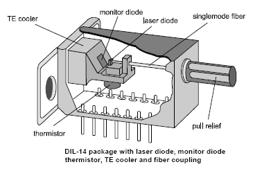
57 Commercial DFB Parameters Symbo l Min Typ Max Unit CW Output power(25c) Pf mw Threshold current It h ma Operating current If ma Forward voltage Vf V Center Wavelength λc nm Linewidth Δ λ MHz Components DFB diode Thermoelectric cooler Thermistor Photodiode Optical isolator Fiber-coupled lens Monitor Current Im μa Monitor dark current(vr=- 5V) Id na Isolation(Optional) Iso db TEC current ITEC A TEC voltage VTEC V Thermistor resistance(at 25 ) Operating Temperature Range Rt h kω To C Storage temperature Tst g C

58 Comparison between LED and LASER
59 PHOTODETECTORS: Photodetectors find applications in the area of medical, automotive, safety and analytical equipments, cameras, communications, astronomy and industry. Types of Photodetectors Photodiode, Photodiode Array, Light Dependent Resistor Avalanche Photodiode Photomultiplier Tube, Microchannel Plate, Image Intensifier Position Sensitive Detector CCD
60 Photodetector Requirements for Performance High sensitivity at the operating wavelength of the source Short response time to obtain a desirable bandwidth Minimum noise contribution Compatible size for efficient coupling and packaging Linear response over a wide range of light intensity Stability of performance characteristics Low bias voltage Low cost
61 Photodetection Mechanisms Photodetector converts light (power) into electrical signals (photocurrent) There are two distinct photodetection mechanisms 1 External photoelectric effect : Photomultiplier Tubes (PMT) 2 Internal photoelectric effect : PN junction photodiodes PIN photodiodes Avalanche photodiodes
62 Principle of Photodetection (In Semiconductor) In semiconductors, conduction band and valence band are separated by a forbidden band gap. Electrons at the valance band are bound. The electrons in the conduction band are free and when small voltage is applied they move and causes current flow Populating the conduction band with electrons causes the semiconductor to conduct current. The value of band gap E g determines the conductive properties of semiconductor


63 Photodetection p n junction in thermal equilibrium with zero bias voltage A PN junction can be formed by diffusing either a P-type impurity such as Boron, into a N-type bulk silicon wafer, or a N-type impurity, such as Phosphorous, into a P-type bulk silicon wafer.
64 Photodetection (a) Photogeneration of e-h pair (b) Reverse biased p-n junction with carrier drift in depletion region (c) Energy band diagram showing photogeneration and separation of e-h pair
65 All semiconductor photodetectors use photon absorption in depletion region to convert photons into electron hole pairs, and then sense them. When a semiconductor is illuminated by light having an energy E = hγ greater than its band gap energy E g the light is absorbed in the semiconductor and electron hole pairs are generated. γ is the frequency of light. Incident photon after passing through p-region will be absorbed in the depletion layer. The absorbed energy creates EHP, Electron raises to conduction band and hole fall to valance band. The free electron travel down the barrier and the free hole will travel up the barrier to constitute current flow. The photon absorbed in the neutral p or n regions, outside the depletion region create EHP, but these free charges will not move quickly due to lack of strong electric field. Most of the free charges will diffuse slowly through the diode and may recombine before reaching the junction. These charges produce negligible current, thus reducing the detector s responsivity.
66 EHP created close to the depletion layer can diffuse and subsequently be swept across the junction by the large electric field due to applied reverse biased voltage. An external current is produced but it is delayed with respect to variations in the incident optical power It is desirable that photon be absorbed in the depletion layer so that it can contribute maximum in generation of photocurrent. Typical pn photodiodes have a rise time of the order of microseconds making them unsuitable for high speed optical systems. The existence of electric field across the junction facilitate the rise of photocurrent The primary operating wavelength regions for FO communication systems are 850nm, 1310nm and 1550 nm. The photodetectors which are used in these systems are : - PN junction photodiodes - PIN photodiodes - Avalanche photodiode

67 Photodetector I-V curve under Illumination The I-V characteristic of a photodiode with no incident light is similar to a rectifying diode. When the photodiode is forward biased, there is an exponential increase in the current. When a reverse bias is applied, a small reverse saturation current appears. It is related to dark current as where I D is the photodiode dark current, I SAT is the reverse saturation current representing thermally generated free carriers which flow through the junction, q is the electron charge, V A is the applied bias voltage, k B =1.38x10⁻²³ J/K, is the Boltzmann Constant and T is the absolute temperature (273 K= 0 o C) I V Illuminating the photodiode with optical radiation, shifts the I-V curve by the amount of photocurrent (I P )

68 Photodiode Characteristics (Electrical) A silicon photodiode can be represented by a current source in parallel with an ideal diode. The diode represents the p-n junction, C j junction capacitance, R SH shunt resistance, R S Series resistance, R L load resistance
69 Shunt resistance: An ideal photodiode should have an infinite R SH, but actual values range from 10 s to 1000 s of Mega ohms. R SH is used to determine the noise current in the photodiode Series resistance: R S of a photodiode arises from the resistance of the contacts and the resistance of the undepleted silicon and its value ranges from 10 to 1000 Ω s. This is used to define the linearity of photodiode. Junction capacitance: The boundaries of the depletion region acts as the plates of a parallel plate capacitor. The junction capacitance is directly proportional to the diffused area and inversely proportional to the width of the depletion region. Junction capacitance is used to determine the speed of the response of the photodiode Response Time: There are three factors defining the response time of a photodiode: 1. t DRIFT, the charge collection time of the carriers in the depleted region of the photodiode. 2. t DIFFUSED, the charge collection time of the carriers in the undepleted region of the photodiode. 3. t RC, the RC time constant of the diode-circuit combination.
 is dependent on the diffused area of the photodiode and the applied reverse bias, faster rise times are obtained with smaller diffused area photodiodes, and")
70 t RC =2.2RC, where R, is the sum of the diode series resistance and the load resistance (R S + R L ), and C, is the sum of the photodiode junction and the stray capacitances (C j +C S ). Since the junction capacitance (C j ) is dependent on the diffused area of the photodiode and the applied reverse bias, faster rise times are obtained with smaller diffused area photodiodes, and larger applied reverse biases. The total rise time is determined by Capacitance of Photoconductive Devices versus Reverse Bias Voltage

71 Photodiode Characteristics (Optical) Responsivity: The responsivity of a silicon photodiode is a measure of the sensitivity to light, and is defined as the ratio of the photocurrent I P to the incident light power P at a given wavelength. It varies with the wavelength of the incident light as well as applied reverse bias and temperature. It is a measure of the effectiveness of the conversion of the light power into electrical current. Temperature Coefficient of Responsivity Vs. Wavelength For Silicon Photodiode The responsivity variations due to change in temperature is due to decrease or increase of the band gap, because of increase or decrease in the temperature respectively
72 Quantum Efficiency (Q.E.) Quantum efficiency is defined as the fraction of the incident photons that contribute to photocurrent. One of the major factor which determine the quantum efficiency is the absorption coefficient of the semiconductor material used within photodetector. < 1 quoted as a percentage say 85% i.e. 85 electrons collected per 100 incident photons It is related to responsivity by
73 Responsivity & Quantum efficiency Quantum Efficiency is not constant at all wavelengthsvaries according to photon energy. Responsivity and quantum efficiency as a function of wavelength for photodiodes constructed from different materials. Comparison of the responsivity and QE as a function of wavelength for photodiodes constructed of different materials. For a given material, as the wavelength of the incident photon becomes larger, the photon energy becomes less than that required to excite an electron from the valence band to the conduction band. Responsivity falls off rapidly beyond cutoff wavelength.
74 Biasing Photodiode Photovoltaic Mode The photovoltaic mode of operation (unbiased) is preferred when a photodiode is used in low frequency applications as well as ultra low light level applications. The photocurrents in this mode have less variations in responsivity with temperature. For stability, select C F such that Operating bandwidth after gain peaking compensation is
75 Photoconductive Mode Application of a reverse bias improves the speed of response. Effect of reverse bias Increase in the depletion region width Decrease in junction capacitance. Increase in the dark and noise currents. Decrease in rise time (t r ). Where GBP is the Gain Bandwidth Product of amplifier (A1) and C A is the amplifier input capacitance. A feedback capacitor (C F ) will limit the frequency response and avoids gain peaking
76 Noise Sources in Photodiode: Shot noise is related to the statistical fluctuation in both the photocurrent and the dark current. Where q=1.6x10⁻¹⁹c, is the electron charge, I P is the photogenerated current, I D is the photodetector dark current and f is the noise measurement bandwidth. Shot noise is the dominating source when operating in photoconductive (biased) mode. Thermal or Johnson Noise The shunt resistance in a photodetector has a Johnson noise associated with it. This is due to the thermal generation of carriers. Where k= 1.38x10⁻²³ J/ºK, is the Boltzmann Constant, T, is the absolute temperature in degrees Kelvin, f is the noise measurement bandwidth and R SH, is the shunt resistance of the photodiode. This type of noise is the dominant current noise in photovoltaic (unbiased) operation mode. All resistors have a Johnson noise associated with them, including the load resistor.
77 Various figure of merit parameters have been used to asses the noise performance of optical detectors. most commonly used are Noise equivalent power (NEP), Detectivity (D) and Specific detectivity (D * ). Noise Equivalent Power (NEP): The minimum input optical power required to generate photocurrent, equal to the rms noise current in a 1Hz bandwidth. NEP is essentially the minimum detectable power. Detectivity(D): The characteristic detectivity (D) is the inverse of NEP, 1/NEP. Specific Detectivity (D*): It is detectivity multiplied by the square root of the area (A) of the photodetector, (D*=D A) for a 1Hz bandwidth. D* allows different photodetectors to be compared independent of sensor area and system bandwidth; a higher detectivity value indicates a low-noise device

78 PIN Photodiode The P-Intrinsic-N structure increases the distance between the P and N conductive layers, decreasing capacitance, increasing speed. The volume of the photo sensitive region also increases, enhancing conversion efficiency. The bandwidth can extend to 10's of GHz. PIN photodiodes are the preferred for high sensitivity, and high speed at moderate cost.
79 P-i-N PHOTODIODE A typical P-i-N photodiode consists of a highly-doped transparent p-type contact layer on top of an undoped absorbing layer (i) and an n-type highly doped contact layer on the bottom. This diode is evolved mainly from one basic requirement: light should be absorbed in the depletion region of the diode to ensure that the electrons and holes are separated in the electric field and contribute to the photocurrent, while the transit time must be minimal. This implies that a depletion region larger than the absorption length must exist in the detector. This is easily assured by making the absorbing layer undoped. Only a very small voltage is required to deplete the undoped region. An added advantage is that the recombination/generation time constant is longest for undoped material, which provides a minimal thermal generation current.
80 Avalanche Photodiodes (APD) Photodetector with Internal gain Avalanche photodiode showing high electric field region Photodiode with Internal gain: Internally multiply the primary signal photocurrent before it enters the input circuitry of the amplifier. Increases receiver sensitivity: the photocurrent is multiplied before encountering the thermal noise associated with the receiver circuit. For carrier multiplication, the photogenerated carriers must traverse a region where a very high electric field is present.
81 In the high field region, a photogenerated electron or hole can gain enough energy so that it ionizes bonds in the valence band upon colliding with them. This is known as Impact Ionization The newly created carriers are also accelerated by the high electric field, gaining enough energy to cause further impact ionization. This phenomenon is the Avalanche Effect Create an extremely high electric field region (approximately 3 x 10 5 V/cm) Requires high reverse bias voltages (100 to 400 V) in order that the new carriers created by impact ionization Carrier multiplication factors as great as 10 4 may be obtained
82 When carriers are generated in undepleted material, they are collected somewhat slowly by the diffusion process. This has the effect of producing a long 'diffusion tail' on a short optical pulse. When the APD is fully depleted by employing high electric fields, all the carriers drift at saturation-limited velocities. The response time for the device is limited by three factors: the transit time of the carriers across the absorption region (i.e. the depletion width) the time taken by the carriers to perform the avalanche multiplication process the RC time constant incurred by the junction capacitance of the diode and its load At low gain the transit time and RC effects dominate giving a definitive response time and hence constant bandwidth for the device At high gain the avalanche build-up time dominates and therefore the device bandwidth decreases proportionately with increasing gain
83 The rise time between ps and fall time of 1ns or more are quite common and this limits the overall response of the device Multiplication factor M is a measure of the internal gain provided by the APD and is defined as M=I M /I P where I M is the average value of the total multiplied output current and I P is the primary photocurrent. The avalanche mechanism is a statistical process, and not every carrier pair generated in the APD experiences the same multiplication. Thus, the measured value of M is expressed as an average quantity which is as great as 10 4.
84 Advantages & Drawbacks of APDs Advantages - Provides an increase in sensitivity of between 5 db to 15dB over p- i-n photodiodes i.e. detection of very low level light signals. - Wider dynamic range as a result of their gain variation with response time and reverse bias Drawbacks - Fabrication difficulties due to their more complex structure and hence increased cost. - The random nature of the gain mechanism which gives an additional noise contribution. - Often high bias voltages required (50 to 400 V) - The variation of the gain (multiplication factor) with temperature i.e. temperature compensation is necessary to stabilize the operation of the device.
85 Photodetectors APD vs p-i-n diode 85
86
Hello and Welcome to this presentation on LED Basics. In this presentation we will look at a few topics in semiconductor lighting such as light
 Hello and Welcome to this presentation on LED Basics. In this presentation we will look at a few topics in semiconductor lighting such as light generation from a semiconductor material, LED chip technology,
AMPLIFIED HIGH SPEED FIBER PHOTODETECTOR USER S GUIDE
 AMPLIFIED HIGH SPEED FIBER PHOTODETECTOR USER S GUIDE Thank you for purchasing your Amplified High Speed Fiber Photodetector. This user s guide will help answer any questions you may have regarding the
3. Diodes and Diode Circuits. 3. Diodes and Diode Circuits TLT-8016 Basic Analog Circuits 2005/2006 1
 3. Diodes and Diode Circuits 3. Diodes and Diode Circuits TLT-8016 Basic Analog Circuits 2005/2006 1 3.1 Diode Characteristics Small-Signal Diodes Diode: a semiconductor device, which conduct the current
Amplified High Speed Fiber Photodetectors
 Amplified High Speed Fiber Photodetectors User Guide (800)697-6782 sales@eotech.com www.eotech.com Page 1 of 7 EOT AMPLIFIED HIGH SPEED FIBER PHOTODETECTOR USER S GUIDE Thank you for purchasing your Amplified
Characteristic and use
 . Basic principle A PSD basically consists of a uniform resistive layer formed on one or both surfaces of a high-resistivity semiconductor substrate, and a pair of electrodes formed on both ends of the
University of California at Santa Cruz Electrical Engineering Department EE-145L: Properties of Materials Laboratory
 University of California at Santa Cruz Electrical Engineering Department EE-145L: Properties of Materials Laboratory Lab 8: Optical Absorption Spring 2002 Yan Zhang and Ali Shakouri, 05/22/2002 (Based
Solid State Detectors = Semi-Conductor based Detectors
 Solid State Detectors = Semi-Conductor based Detectors Materials and their properties Energy bands and electronic structure Charge transport and conductivity Boundaries: the p-n junction Charge collection
Avalanche Photodiodes: A User's Guide
 !"#$%& Abstract Avalanche Photodiodes: A User's Guide Avalanche photodiode detectors have and will continue to be used in many diverse applications such as laser range finders and photon correlation studies.
(Amplifying) Photo Detectors: Avalanche Photodiodes Silicon Photomultiplier
 Photo Detectors: Avalanche Photodiodes Silicon Photomultiplier") (Amplifying) Photo Detectors: Avalanche Photodiodes Silicon Photomultiplier (no PiN and pinned Diodes) Peter Fischer P. Fischer, ziti, Uni Heidelberg, Seite 1 Overview Reminder: Classical Photomultiplier
(Amplifying) Photo Detectors: Avalanche Photodiodes Silicon Photomultiplier (no PiN and pinned Diodes) Peter Fischer P. Fischer, ziti, Uni Heidelberg, Seite 1 Overview Reminder: Classical Photomultiplier
Robert G. Hunsperger. Integrated Optics. Theory and Technology. Fourth Edition. With 195 Figures and 17 Tables. Springer
 Robert G. Hunsperger Integrated Optics Theory and Technology Fourth Edition With 195 Figures and 17 Tables Springer Contents 1. Introduction 1 1.1 Advantages of Integrated Optics 2 1.1.1 Comparison of
The Physics of Energy sources Renewable sources of energy. Solar Energy
 The Physics of Energy sources Renewable sources of energy Solar Energy B. Maffei Bruno.maffei@manchester.ac.uk Renewable sources 1 Solar power! There are basically two ways of using directly the radiative
PUMPED Nd:YAG LASER. Last Revision: August 21, 2007
 PUMPED Nd:YAG LASER Last Revision: August 21, 2007 QUESTION TO BE INVESTIGATED: How can an efficient atomic transition laser be constructed and characterized? INTRODUCTION: This lab exercise will allow
6.772/SMA5111 - Compound Semiconductors Lecture 18 - Light Emitting Diodes - Outline
 6.772/SMA5111 - Compound Semiconductors Lecture 18 - Light Emitting Diodes - Outline Recombination Processes (continued from Lecture 17) Radiative vs. non-radiative Relative carrier lifetimes Light emitting
Special-Purpose Diodes
 7 Special-Purpose Diodes 7.1 Zener Diode 7.2 Light-Emitting Diode (LED) 7.3 LED Voltage and Current 7.4 Advantages of LED 7.5 Multicolour LEDs 7.6 Applications of LEDs 7.7 Photo-diode 7.8 Photo-diode operation
Fiber Optics: Fiber Basics
 Photonics Technical Note # 21 Fiber Optics Fiber Optics: Fiber Basics Optical fibers are circular dielectric wave-guides that can transport optical energy and information. They have a central core surrounded
Lecture 12: Photodiode detectors
 Lecture 12: Photodiode detectors Background concepts p-n photodiodes Photoconductive/photovoltaic modes p-i-n photodiodes Responsivity and bandwidth Noise in photodetectors References: This lecture partially
Project 2B Building a Solar Cell (2): Solar Cell Performance
: Solar Cell Performance") April. 15, 2010 Due April. 29, 2010 Project 2B Building a Solar Cell (2): Solar Cell Performance Objective: In this project we are going to experimentally measure the I-V characteristics, energy conversion
April. 15, 2010 Due April. 29, 2010 Project 2B Building a Solar Cell (2): Solar Cell Performance Objective: In this project we are going to experimentally measure the I-V characteristics, energy conversion
Solar Cell Parameters and Equivalent Circuit
 9 Solar Cell Parameters and Equivalent Circuit 9.1 External solar cell parameters The main parameters that are used to characterise the performance of solar cells are the peak power P max, the short-circuit
FUNDAMENTAL PROPERTIES OF SOLAR CELLS
 FUNDAMENTAL PROPERTIES OF SOLAR CELLS January 31, 2012 The University of Toledo, Department of Physics and Astronomy SSARE, PVIC Principles and Varieties of Solar Energy (PHYS 4400) and Fundamentals of
Yrd. Doç. Dr. Aytaç Gören
 H2 - AC to DC Yrd. Doç. Dr. Aytaç Gören ELK 2018 - Contents W01 Basic Concepts in Electronics W02 AC to DC Conversion W03 Analysis of DC Circuits W04 Transistors and Applications (H-Bridge) W05 Op Amps
FEATURE ARTICLE. Figure 1: Current vs. Forward Voltage Curves for Silicon Schottky Diodes with High, Medium, Low and ZBD Barrier Heights
 PAGE 1 FEBRUARY 2009 Schottky Diodes by Rick Cory, Skyworks Solutions, Inc. Introduction Schottky diodes have been used for several decades as the key elements in frequency mixer and RF power detector
# 2. Selecting and Using Thermistors for Temperature Control
 # 2 Selecting and Using Thermistors for Temperature Control Selecting and Using Thermistors for Temperature Control Thermally sensitive resistors (thermistors) are used widely in laser diode and detector
Technology Developments Towars Silicon Photonics Integration
 Technology Developments Towars Silicon Photonics Integration Marco Romagnoli Advanced Technologies for Integrated Photonics, CNIT Venezia - November 23 th, 2012 Medium short reach interconnection Example:
Prospects for Solar Pumped Semiconductor Lasers Geoffrey A. Landis
 Paper SPIE 2121-09, Laser Power Beaming, SPIE Proceedings Volume 2121, pp. 58-65 (1994). Presented at SPIE Optics, Electro-optics & Laser Conference, Los Angeles CA, January 27-28 1994 Prospects for Solar
Characteristic curves of a solar cell
 Related Topics Semi-conductor, p-n junction, energy-band diagram, Fermi characteristic energy level, diffusion potential, internal resistance, efficiency, photo-conductive effect, acceptors, donors, valence
Helium-Neon Laser. Figure 1: Diagram of optical and electrical components used in the HeNe laser experiment.
 Helium-Neon Laser Experiment objectives: assemble and align a 3-mW HeNe laser from readily available optical components, record photographically the transverse mode structure of the laser output beam,
4.3.5: High Temperature Test 3
 temperature and 800 degrees Celsius is made by matching the optical path lengths of the measurement and sensing arms at both temperatures. By marking the relative distance between the GRIN lens and mirror
Efficiency of a Light Emitting Diode
 PHYSICS THROUGH TEACHING LABORATORY VII Efficiency of a Light Emitting Diode RAJESH B. KHAPARDE AND SMITHA PUTHIYADAN Homi Bhabha Centre for Science Education Tata Institute of Fundamental Research V.
Optical Detectors and Human Vision
 F UNDAMENTALS OF PHOTONICS Module 1.6 Optical Detectors and Human Vision Jack Ready Consultant, formerly with Honeywell Technology Center Edina, Minnesota Many photonics applications require the use of
ENEE 313, Spr 09 Midterm II Solution
 ENEE 313, Spr 09 Midterm II Solution PART I DRIFT AND DIFFUSION, 30 pts 1. We have a silicon sample with non-uniform doping. The sample is 200 µm long: In the figure, L = 200 µm= 0.02 cm. At the x = 0
Understanding the p-n Junction by Dr. Alistair Sproul Senior Lecturer in Photovoltaics The Key Centre for Photovoltaic Engineering, UNSW
 Understanding the p-n Junction by Dr. Alistair Sproul Senior Lecturer in Photovoltaics The Key Centre for Photovoltaic Engineering, UNSW The p-n junction is the fundamental building block of the electronic
Fundamentals of modern UV-visible spectroscopy. Presentation Materials
 Fundamentals of modern UV-visible spectroscopy Presentation Materials The Electromagnetic Spectrum E = hν ν = c / λ 1 Electronic Transitions in Formaldehyde 2 Electronic Transitions and Spectra of Atoms
High Open Circuit Voltage of MQW Amorphous Silicon Photovoltaic Structures
 High Open Circuit Voltage of MQW Amorphous Silicon Photovoltaic Structures ARGYRIOS C. VARONIDES Physics and EE Department University of Scranton 800 Linden Street, Scranton PA, 18510 United States Abstract:
Solid-State Physics: The Theory of Semiconductors (Ch. 10.6-10.8) SteveSekula, 30 March 2010 (created 29 March 2010)
 SteveSekula, 30 March 2010 (created 29 March 2010)") Modern Physics (PHY 3305) Lecture Notes Modern Physics (PHY 3305) Lecture Notes Solid-State Physics: The Theory of Semiconductors (Ch. 10.6-10.8) SteveSekula, 30 March 2010 (created 29 March 2010) Review
Modern Physics (PHY 3305) Lecture Notes Modern Physics (PHY 3305) Lecture Notes Solid-State Physics: The Theory of Semiconductors (Ch. 10.6-10.8) SteveSekula, 30 March 2010 (created 29 March 2010) Review
Experiment 5. Lasers and laser mode structure
 Northeastern University, PHYS5318 Spring 2014, 1 1. Introduction Experiment 5. Lasers and laser mode structure The laser is a very important optical tool that has found widespread use in science and industry,
Energy band diagrams. Single atom. Crystal. Excited electrons cannot move. Excited electrons can move (free electrons)
") Energy band diagrams In the atoms, the larger the radius, the higher the electron potential energy Hence, electron position can be described either by radius or by its potential energy In the semiconductor
Energy band diagrams In the atoms, the larger the radius, the higher the electron potential energy Hence, electron position can be described either by radius or by its potential energy In the semiconductor
Recent developments in high bandwidth optical interconnects. Brian Corbett. www.tyndall.ie
 Recent developments in high bandwidth optical interconnects Brian Corbett Outline Introduction to photonics for interconnections Polymeric waveguides and the Firefly project Silicon on insulator (SOI)
Module 13 : Measurements on Fiber Optic Systems
 Module 13 : Measurements on Fiber Optic Systems Lecture : Measurements on Fiber Optic Systems Objectives In this lecture you will learn the following Measurements on Fiber Optic Systems Attenuation (Loss)
ILX Lightwave Corporation www.ilxlightwave.com
 # 14 Optimizing TEC Current Optimizing TEC Drive Current This Application Note discusses methods for optimizing the TEC drive current for optimum operation in heating and cooling applications. BACKGROUND
High-Performance Wavelength-Locked Diode Lasers
 Copyright 29 Society of Photo-Optical Instrumentation Engineers. This paper was published in the proceedings of the SPIE Photonics West 29, Vol. 7198-38 (29), High-Power Diode Laser Technology and High-Performance
LLAM Series 900/1060/1550/1550E Si and InGaAs Low-Light Analog APD Receiver Modules (LLAM)
") DATASHEET Photon Detection LLAM Series 900/60/15/15E Excelitas LLAM-15E InGasAs APD Preamplifier Modules exhibit enhanced damage threshold and greater resilience when exposed to higher optical power densities.
DATASHEET Photon Detection LLAM Series 900/60/15/15E Excelitas LLAM-15E InGasAs APD Preamplifier Modules exhibit enhanced damage threshold and greater resilience when exposed to higher optical power densities.
Analog Optical Isolators VACTROLS
 Analog Optical Isolators VACTROLS What Are Analog Optical Isolators? PerkinElmer Optoelectronics has been a leading manufacturer of analog optical isolators for over twenty years and makes a broad range
Silicon, the test mass substrate of tomorrow? Jerome Degallaix The Next Detectors for Gravitational Wave Astronomy Beijing - 2015
 Silicon, the test mass substrate of tomorrow? Jerome Degallaix The Next Detectors for Gravitational Wave Astronomy Beijing - 2015 Program of the talk... What we have now What we know about silicon What
Blackbody Radiation References INTRODUCTION
 Blackbody Radiation References 1) R.A. Serway, R.J. Beichner: Physics for Scientists and Engineers with Modern Physics, 5 th Edition, Vol. 2, Ch.40, Saunders College Publishing (A Division of Harcourt
Chapter 5. Second Edition ( 2001 McGraw-Hill) 5.6 Doped GaAs. Solution
 5.6 Doped GaAs. Solution") Chapter 5 5.6 Doped GaAs Consider the GaAs crystal at 300 K. a. Calculate the intrinsic conductivity and resistivity. Second Edition ( 2001 McGraw-Hill) b. In a sample containing only 10 15 cm -3 ionized
Chapter 5 5.6 Doped GaAs Consider the GaAs crystal at 300 K. a. Calculate the intrinsic conductivity and resistivity. Second Edition ( 2001 McGraw-Hill) b. In a sample containing only 10 15 cm -3 ionized
CHAPTER 10 Fundamentals of the Metal Oxide Semiconductor Field Effect Transistor
 CHAPTER 10 Fundamentals of the Metal Oxide Semiconductor Field Effect Transistor Study the characteristics of energy bands as a function of applied voltage in the metal oxide semiconductor structure known
Programmable-Gain Transimpedance Amplifiers Maximize Dynamic Range in Spectroscopy Systems
 Programmable-Gain Transimpedance Amplifiers Maximize Dynamic Range in Spectroscopy Systems PHOTODIODE VOLTAGE SHORT-CIRCUIT PHOTODIODE SHORT- CIRCUIT VOLTAGE 0mV DARK ark By Luis Orozco Introduction Precision
Vertical Cavity Surface Emitting Laser OPV300, OPV310, OPV310Y, OPV314, OPV314Y
 Features: 850nm Technology Data rates up to 2.5 Gbps High thermal stability Low drive current / high output density Narrow and concentric beam angle Recommended for mul mode fiber applica ons Burned in
High Resolution Spatial Electroluminescence Imaging of Photovoltaic Modules
 High Resolution Spatial Electroluminescence Imaging of Photovoltaic Modules Abstract J.L. Crozier, E.E. van Dyk, F.J. Vorster Nelson Mandela Metropolitan University Electroluminescence (EL) is a useful
APPLICATION NOTES: Dimming InGaN LED
 APPLICATION NOTES: Dimming InGaN LED Introduction: Indium gallium nitride (InGaN, In x Ga 1-x N) is a semiconductor material made of a mixture of gallium nitride (GaN) and indium nitride (InN). Indium
Semiconductors, diodes, transistors
 Semiconductors, diodes, transistors (Horst Wahl, QuarkNet presentation, June 2001) Electrical conductivity! Energy bands in solids! Band structure and conductivity Semiconductors! Intrinsic semiconductors!
Optical Communications
 Optical Communications Telecommunication Engineering School of Engineering University of Rome La Sapienza Rome, Italy 2005-2006 Lecture #2, May 2 2006 The Optical Communication System BLOCK DIAGRAM OF
Laboratory #3 Guide: Optical and Electrical Properties of Transparent Conductors -- September 23, 2014
 Laboratory #3 Guide: Optical and Electrical Properties of Transparent Conductors -- September 23, 2014 Introduction Following our previous lab exercises, you now have the skills and understanding to control
Introduction to Optical Link Design
 University of Cyprus Πανεπιστήµιο Κύπρου 1 Introduction to Optical Link Design Stavros Iezekiel Department of Electrical and Computer Engineering University of Cyprus HMY 445 Lecture 08 Fall Semester 2014
THE CURRENT-VOLTAGE CHARACTERISTICS OF AN LED AND A MEASUREMENT OF PLANCK S CONSTANT Physics 258/259
 DSH 2004 THE CURRENT-VOLTAGE CHARACTERISTICS OF AN LED AND A MEASUREMENT OF PLANCK S CONSTANT Physics 258/259 I. INTRODUCTION Max Planck (1858-1947) was an early pioneer in the field of quantum physics.
Solar Photovoltaic (PV) Cells
 Cells") Solar Photovoltaic (PV) Cells A supplement topic to: Mi ti l S Micro-optical Sensors - A MEMS for electric power generation Science of Silicon PV Cells Scientific base for solar PV electric power generation
Solar Photovoltaic (PV) Cells A supplement topic to: Mi ti l S Micro-optical Sensors - A MEMS for electric power generation Science of Silicon PV Cells Scientific base for solar PV electric power generation
LAB IV. SILICON DIODE CHARACTERISTICS
 LAB IV. SILICON DIODE CHARACTERISTICS 1. OBJECTIVE In this lab you are to measure I-V characteristics of rectifier and Zener diodes in both forward and reverse-bias mode, as well as learn to recognize
Single Photon Counting Module COUNT -Series
 Description Laser Components COUNT series of s has been developed to offer a unique combination of high photon detection efficiency, wide dynamic range and ease of use for photon counting applications.
CONTENTS. Preface. 1.1.2. Energy bands of a crystal (intuitive approach)
") CONTENTS Preface. Energy Band Theory.. Electron in a crystal... Two examples of electron behavior... Free electron...2. The particle-in-a-box approach..2. Energy bands of a crystal (intuitive approach)..3.
CONTENTS Preface. Energy Band Theory.. Electron in a crystal... Two examples of electron behavior... Free electron...2. The particle-in-a-box approach..2. Energy bands of a crystal (intuitive approach)..3.
Diodes and Transistors
 Diodes What do we use diodes for? Diodes and Transistors protect circuits by limiting the voltage (clipping and clamping) turn AC into DC (voltage rectifier) voltage multipliers (e.g. double input voltage)
2 Absorbing Solar Energy
 2 Absorbing Solar Energy 2.1 Air Mass and the Solar Spectrum Now that we have introduced the solar cell, it is time to introduce the source of the energy the sun. The sun has many properties that could
Discontinued. LUXEON V Portable. power light source. Introduction
 Preliminary Technical Datasheet DS40 power light source LUXEON V Portable Introduction LUXEON is a revolutionary, energy efficient and ultra compact new light source, combining the lifetime and reliability
Vacuum Evaporation Recap
 Sputtering Vacuum Evaporation Recap Use high temperatures at high vacuum to evaporate (eject) atoms or molecules off a material surface. Use ballistic flow to transport them to a substrate and deposit.
A More Efficient Way to De-shelve 137 Ba +
 A More Efficient Way to De-shelve 137 Ba + Abstract: Andrea Katz Trinity University UW REU 2010 In order to increase the efficiency and reliability of de-shelving barium ions, an infrared laser beam was
SpectraTec II. Polarized Multi-Laser Source BLUE SKY RESEARCH WAVELENGTHS. The SpectraTec II
 BLUE SKY RESEARCH The SpectraTec II, two wavelength laser module is a highly integrated system comprised of two lasers, individual driving and temperature control electronics, wavelength combining, and
Data Sheet. HFBR-0600Z Series SERCOS Fiber Optic Transmitters and Receivers
 HFBR-0600Z Series SERCOS Fiber Optic Transmitters and Receivers Data Sheet SERCOS SERCOS is a SErial Realtime COmmunication System, a standard digital interface for communication between controls and drives
Basics of LED drivers. Functions Requirements Selection
 Andreas Hagemeyer Master of Science 05.2015 This article is meant to provide the reader with basic knowledge about the functional principle of LED luminaires, to explain the requirements for an LED driver
Application Notes FREQUENCY LINEAR TUNING VARACTORS FREQUENCY LINEAR TUNING VARACTORS THE DEFINITION OF S (RELATIVE SENSITIVITY)
") FREQUENY LINEAR TUNING VARATORS FREQUENY LINEAR TUNING VARATORS For several decades variable capacitance diodes (varactors) have been used as tuning capacitors in high frequency circuits. Most of these
FREQUENY LINEAR TUNING VARATORS FREQUENY LINEAR TUNING VARATORS For several decades variable capacitance diodes (varactors) have been used as tuning capacitors in high frequency circuits. Most of these
Op Amp Circuit Collection
 Op Amp Circuit Collection Note: National Semiconductor recommends replacing 2N2920 and 2N3728 matched pairs with LM394 in all application circuits. Section 1 Basic Circuits Inverting Amplifier Difference
Low Noise, Matched Dual PNP Transistor MAT03
 a FEATURES Dual Matched PNP Transistor Low Offset Voltage: 100 V Max Low Noise: 1 nv/ Hz @ 1 khz Max High Gain: 100 Min High Gain Bandwidth: 190 MHz Typ Tight Gain Matching: 3% Max Excellent Logarithmic
Silicon Drift Detector Product Brochure Update 2013
 Silicon Drift Detector Product Brochure Update 2013 Content Classic Silicon Drift Detector High Resolution Silicon Drift Detector Multielement Silicon Detector Extra Large Detector Series July 2013 About
Crystalline solids. A solid crystal consists of different atoms arranged in a periodic structure.
 Crystalline solids A solid crystal consists of different atoms arranged in a periodic structure. Crystals can be formed via various bonding mechanisms: Ionic bonding Covalent bonding Metallic bonding Van
Diode Circuits. Operating in the Reverse Breakdown region. (Zener Diode)
") Diode Circuits Operating in the Reverse Breakdown region. (Zener Diode) In may applications, operation in the reverse breakdown region is highly desirable. The reverse breakdown voltage is relatively insensitive
Diode Circuits Operating in the Reverse Breakdown region. (Zener Diode) In may applications, operation in the reverse breakdown region is highly desirable. The reverse breakdown voltage is relatively insensitive
0.00 18 TO18 0.00 _ nothing special M 0.20 49.00 A UVA 24.00 18ISO90 TO18 6.00 Lens concentr. Lens D 0.50 49.00 B UVB 24.
 Basic Information That guide assists you selecting the right ilicon Carbide (ic) based UV photodiode for your application. Basically this selection is between active area, spectral behaviour, packaging
Features. Applications
 LM555 Timer General Description The LM555 is a highly stable device for generating accurate time delays or oscillation. Additional terminals are provided for triggering or resetting if desired. In the
Power Supplies. 1.0 Power Supply Basics. www.learnabout-electronics.org. Module
 Module 1 www.learnabout-electronics.org Power Supplies 1.0 Power Supply Basics What you ll learn in Module 1 Section 1.0 Power Supply Basics. Basic functions of a power supply. Safety aspects of working
BJT Characteristics and Amplifiers
 BJT Characteristics and Amplifiers Matthew Beckler beck0778@umn.edu EE2002 Lab Section 003 April 2, 2006 Abstract As a basic component in amplifier design, the properties of the Bipolar Junction Transistor
Synthetic Sensing: Proximity / Distance Sensors
 Synthetic Sensing: Proximity / Distance Sensors MediaRobotics Lab, February 2010 Proximity detection is dependent on the object of interest. One size does not fit all For non-contact distance measurement,
- thus, the total number of atoms per second that absorb a photon is
 Stimulated Emission of Radiation - stimulated emission is referring to the emission of radiation (a photon) from one quantum system at its transition frequency induced by the presence of other photons
Chip Diode Application Note
 Chip Diode Application Note Introduction The markets of portable communications, computing and video equipment are challenging the semiconductor industry to develop increasingly smaller electronic components.
UNIT I: INTRFERENCE & DIFFRACTION Div. B Div. D Div. F INTRFERENCE
 107002: EngineeringPhysics Teaching Scheme: Lectures: 4 Hrs/week Practicals-2 Hrs./week T.W.-25 marks Examination Scheme: Paper-50 marks (2 hrs) Online -50marks Prerequisite: Basics till 12 th Standard
Nanoscale Resolution Options for Optical Localization Techniques. C. Boit TU Berlin Chair of Semiconductor Devices
 berlin Nanoscale Resolution Options for Optical Localization Techniques C. Boit TU Berlin Chair of Semiconductor Devices EUFANET Workshop on Optical Localization Techniques Toulouse, Jan 26, 2009 Jan 26,
Broadband THz Generation from Photoconductive Antenna
 Progress In Electromagnetics Research Symposium 2005, Hangzhou, China, August 22-26 331 Broadband THz Generation from Photoconductive Antenna Qing Chang 1, Dongxiao Yang 1,2, and Liang Wang 1 1 Zhejiang
Activitity (of a radioisotope): The number of nuclei in a sample undergoing radioactive decay in each second. It is commonly expressed in curies
: The number of nuclei in a sample undergoing radioactive decay in each second. It is commonly expressed in curies") Activitity (of a radioisotope): The number of nuclei in a sample undergoing radioactive decay in each second. It is commonly expressed in curies (Ci), where 1 Ci = 3.7x10 10 disintegrations per second.
Activitity (of a radioisotope): The number of nuclei in a sample undergoing radioactive decay in each second. It is commonly expressed in curies (Ci), where 1 Ci = 3.7x10 10 disintegrations per second.
High-Reliability Diode Lasers for Gesture Recognition. Applying Telecommunications Reliability Design to Consumer Electronics
 High-Reliability Diode Lasers for Gesture Recognition Applying Telecommunications Reliability Design to Consumer Electronics www.lumentum.com Application Note A wide range of consumer-electronics applications
Small Optical Encoder Modules 480lpi Digital Output. Features. Applications VCC 3 CHANNEL A 2 CHANNEL B 4 GND 1
 HEDS-9730, HEDS-9731 Small Optical Encoder Modules 480lpi Digital Output Data Sheet Description The HEDS-973X is a high performance incremental encoder module. When operated in conjunction with either
# 33. Estimating Laser Diode Lifetimes and Activation Energy
 # 33 Estimating Laser Diode Lifetimes and Activation Energy Estimating Laser Diode Lifetimes and Activation Energy By: Patrick Gale Introduction The estimation of laser diode lifetime is important to both
Optical Fibres. Introduction. Safety precautions. For your safety. For the safety of the apparatus
 Please do not remove this manual from from the lab. It is available at www.cm.ph.bham.ac.uk/y2lab Optics Introduction Optical fibres are widely used for transmitting data at high speeds. In this experiment,
AMPLIFIERS BJT BJT TRANSISTOR. Types of BJT BJT. devices that increase the voltage, current, or power level
 AMPLFERS Prepared by Engr. JP Timola Reference: Electronic Devices by Floyd devices that increase the voltage, current, or power level have at least three terminals with one controlling the flow between
LM118/LM218/LM318 Operational Amplifiers
 LM118/LM218/LM318 Operational Amplifiers General Description The LM118 series are precision high speed operational amplifiers designed for applications requiring wide bandwidth and high slew rate. They
Volumes. Goal: Drive optical to high volumes and low costs
 First Electrically Pumped Hybrid Silicon Laser Sept 18 th 2006 The information in this presentation is under embargo until 9/18/06 10:00 AM PST 1 Agenda Dr. Mario Paniccia Director, Photonics Technology
Application Note AN1
 TAKING INVENTIVE STEPS IN INFRARED. MINIATURE INFRARED GAS SENSORS GOLD SERIES UK Patent App. No. 799A USA Patent App. No. 9/78,7 World Patents Pending SENSOR OVERVIEW Application Note AN The Dynament
DIRECTIONAL FIBER OPTIC POWER MONITORS (TAPS/PHOTODIODES)
") Features: DIRECTIONAL FIBER OPTIC POWER MONITORS (TAPS/PHOTODIODES) PATENT NUMBERS: CANADA 2,494,133, USA 7095931, 7295731 AND CHINA 1672073 Telcordia GR-468 qualified Available in versions for any wavelength
Features: DIRECTIONAL FIBER OPTIC POWER MONITORS (TAPS/PHOTODIODES) PATENT NUMBERS: CANADA 2,494,133, USA 7095931, 7295731 AND CHINA 1672073 Telcordia GR-468 qualified Available in versions for any wavelength
BPW34. Silicon PIN Photodiode VISHAY. Vishay Semiconductors
 Silicon PIN Photodiode Description The is a high speed and high sensitive PIN photodiode in a miniature flat plastic package. Its top view construction makes it ideal as a low cost replacement of TO-5
E. K. A. ADVANCED PHYSICS LABORATORY PHYSICS 3081, 4051 NUCLEAR MAGNETIC RESONANCE
 E. K. A. ADVANCED PHYSICS LABORATORY PHYSICS 3081, 4051 NUCLEAR MAGNETIC RESONANCE References for Nuclear Magnetic Resonance 1. Slichter, Principles of Magnetic Resonance, Harper and Row, 1963. chapter
Raman Spectroscopy Basics
 Raman Spectroscopy Basics Introduction Raman spectroscopy is a spectroscopic technique based on inelastic scattering of monochromatic light, usually from a laser source. Inelastic scattering means that
Silicon Schottky Barrier Diode Bondable Chips and Beam Leads
 DATA SHEET Silicon Schottky Barrier Diode Bondable Chips and Beam Leads Applications Detectors Mixers Features Available in both P-type and N-type low barrier designs Low 1/f noise Large bond pad chip
Gamma and X-Ray Detection
 Gamma and X-Ray Detection DETECTOR OVERVIEW The kinds of detectors commonly used can be categorized as: a. Gas-filled Detectors b. Scintillation Detectors c. Semiconductor Detectors The choice of a particular
Copyright 1999 2010 by Mark Brandt, Ph.D. 12
 Introduction to Absorbance Spectroscopy A single beam spectrophotometer is comprised of a light source, a monochromator, a sample holder, and a detector. An ideal instrument has a light source that emits
Figure 1. Diode circuit model
 Semiconductor Devices Non-linear Devices Diodes Introduction. The diode is two terminal non linear device whose I-V characteristic besides exhibiting non-linear behavior is also polarity dependent. The