ELEC 6740 Electronics Manufacturing Chapter 7: Design for Manufacturability, Testing & Repair
|
|
|
- Pierce Hardy
- 7 years ago
- Views:
Transcription
1 ELEC 6740 Electronics Manufacturing Chapter 7: Design for Manufacturability, Testing & Repair R. Wayne Johnson Auburn
2 Outline! DFM Organizational Structure! General Design Considerations! Component Selection Considerations for Manufacturability! Soldering Considerations! Interpackage Spacing Considerations! Via Hole Considerations! Soldermask Considerations! Repairability Considerations! Cleanliness Considerations! Testability Considerations
3 DFM Organizational Structure! Sequential design vs. concurrent engineering Physical layout Manufacturing Test Design Physical layout Logic design Manufacturing Product engineers Design Reliability enginesrs Test Process engineers
4 General Design Considerations! Standard form factor (board size, shape, tooling holes)! Odd shapes can require special fixtures, etc.! Standard assembly panel size vs. board size!optimization of boards per assembly panel!optimization of assembly panels per PWB panel!l/w < 1.5
5 Scoring of Panels
6 Fiducials or Alignment Marks
7 Fiducials or Alignment Marks
8 Component Selection! Use surface mount components that solve real estate constraints or reduce the number of manufacturing steps and bear no cost premium.! All surface mount components should be autoplaceable! Tantalum caps with welded studs! Connectors! Heat sinks! Sockets
9 Component Selection! Components terminations with solder plating are better than solder dipped! Select only components that can withstand the reflow temperatures! Use 1206 and 0805 components when possible, 0603, 0402 & 0201 components are harder to place! Use X7R capacitors rather than Z5U when using wave soldering to avoid cracking
10 Component Selection! Do not wave solder capacitors larger than 1812 to avoid cracking! Do not use ceramic parts larger than on FR-4 4 to avoid CTE mismatch and potential reliability concerns! Use marked components if no cost premium! For secondary side attachment in Type II or Type III SMT use low profile SOT devices instead of high profile SOTs.. Low profile are easier for adhesive attachment, but high profile are easier to clean
11 Component Selection! Avoid using MELF packages unless very cost driven (MELF package cheaper)! Use Nickel barrier terminated capacitors and resistors to prevent leaching of termination into molten solder! Avoid surface mount connectors & sockets without over riding reasons
12 Component Selection! Use qualified parts! Minimize the different types of components
13 Soldering Considerations
14 ! Options Soldering Considerations! Double sided reflow + hand soldering! Reflow side 1 & wave solder side 2! May degrade reliability of side 2 SMT components during wave solder! Flux can creep into SOIC and PLCC packages! Double sided reflow with DIP using butt joints! Reliability of butt joint! Not permitted for military and high reliability applications! Double sided reflow with paste-in in-hole! Reflow side 1 & wave solder side 2 with shield
15 Wave Solder Shield
16 Solder Shield! Stainless Steel or Titanium! Titanium expensive & hard to machine but holds shape better for repeated use! Aluminum or copper shield contaminates solder pot! High temperature plastics and composites are also used
17 Savings by Converting SMT
18 No Savings by Converting
19 Other Soldering Considerations! Place larger components on top (2 nd ) reflow side when using double sided reflow! Wave solder is not cheaper than reflow so wave solder can be considered if only SMT passives on 1 side! Wave solder fills plated through holes allowing vacuum to hold board down for automated test
20 Component Orientation
21 Component Orientation
22 Component Orientation
23 Component Orientation
24 Component Orientation
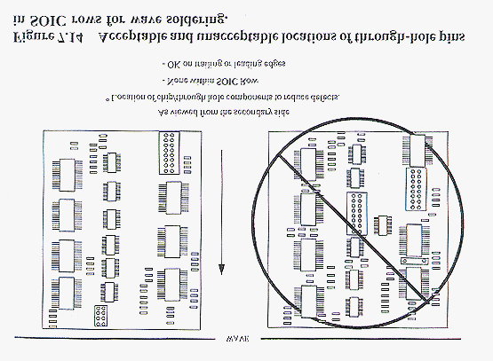
25 Component Orientation
26 Interpackage Spacing! Use land patterns described in Chapter 6! For mixed assemblies, autoinsert equipment requires about clearance for through hole devices! About to clearance is needed for automated and hand probe testing! The interpackage spacing must allow for test probe at ATE.
27 Interpackage Spacing! Automated cleaning with adequate pressure nozzles (>30psi)! Component shift during reflow soldering and placement may be up to 25% of the pad width for military and 50% for commercial applications! Solder joint melting of adjacent components is allowed a total of 4 times (2 for assembly and 2 for rework)! Visual inspection ( board tilting)
28 Interpackage Spacing
29 Interpackage Spacing
30 Interpackage Spacing
31 Interpackage Spacing
32 Interpackage Spacing
33 Via Holes! Number decreased with switch to SMT, but did not go away! SMT vias are smaller than Through Holes for components! Vias are used for test probe contact! Vias must be filled (solder or solder mask) for vacuum used in bed-of of-nails ATE.! Vias should not be used in SMT pads! Via hole location a concern in reflow due to limited solder volume, but not in wave solder
34 Via Holes
35 Via Holes
36 Via Holes
37 Tented Vias
38 ! Dry film Tented Vias! Should not be used between pads of chip components! thick can lead to tombstoning! Thinner dry film can be used! Allows tenting
39 ! Wet film Tented Vias! Thinner, allows traces to be run between pads of passive components! Vias must be plugged before tenting! Increases adhesive bond strength, and minimizes voids during adhesive cure
40 Solder Mask! Solder mask should not be used over Sn/Pb!Solder melts during reflow causing solder mask to crack entrapping flux and moisture! SMOBC solder mask over bare copper
41 Repairability! Hand repair! Automated systems with hot air! Maximum of 2 rework cycles to limit Sn-Cu intermetallic formation
42 Repairability
43 Repairability
44 Testability
45 Testing! In through hole technology, all leads are accessible on the bottom side of the board! With SMT, test points must be provided for in- circuit test! Test point take up space! No test point, no in-circuit test! Functional vs. In-circuit
46 ATE! Use 1 test point (TP) for ground and 1 TP for power for every 10 ICs to reduce risk of ringing! Connect all unused pins to ground or power via a resistor to improve quality of test! Whenever possible, avoid double sided test probe approach to reduce fixturing and cost! One TP is needed for every test node unless 100% capability is needed for individual components
47 ATE! Test point spacings should be whenever possible. Probes for smaller spacings are fragile and prone to damage! For smaller TPs (under 30 mils dia.) deposit solder paste on the TPs to form bumps for ease of probing with serrated test probes! Flux residue can interfere with probe contact
48 ATE
 Preface xiii Introduction xv 1 Planning for surface mount design General electronic products 3 Dedicated service electronic products 3 High-reliability electronic products 4 Defining the environmental
Good Boards = Results
 Section 2: Printed Circuit Board Fabrication & Solderability Good Boards = Results Board fabrication is one aspect of the electronics production industry that SMT assembly engineers often know little about.
How to Build a Printed Circuit Board. Advanced Circuits Inc 2004
 How to Build a Printed Circuit Board 1 This presentation is a work in progress. As methods and processes change it will be updated accordingly. It is intended only as an introduction to the production
Leaded Surface Mount Technology (SMT) 7
 7") Leaded Surface Mount Technology (SMT) 7 7.1 Introduction Traditional through-hole Dual In-Line Package assemblies reached their limits in terms of improvements in cost, weight, volume, and reliability
Leaded Surface Mount Technology (SMT) 7 7.1 Introduction Traditional through-hole Dual In-Line Package assemblies reached their limits in terms of improvements in cost, weight, volume, and reliability
Acceptability of Printed Circuit Board Assemblies
 Section No.: 12I.2.3, Sheet 1 of 9 Rev Level: 16 Additional Distribution: PCB Assembly Subcontractors 1.0 Purpose 2.0 Scope Acceptability of Printed Circuit Board Assemblies 1.1 The purpose of this standard
What is surface mount?
 A way of attaching electronic components to a printed circuit board The solder joint forms the mechanical and electrical connection What is surface mount? Bonding of the solder joint is to the surface
Assembly of LPCC Packages AN-0001
 Assembly of LPCC Packages AN-0001 Surface Mount Assembly and Handling of ANADIGICS LPCC Packages 1.0 Overview ANADIGICS power amplifiers are typically packaged in a Leadless Plastic Chip Carrier (LPCC)
A and M Electronics Contract Manufacturing Circuit Board Assembly 25018 Avenue Kearny Valencia, Ca. 91355 (661) 257-3680 or (800) 923-3058
 257-3680 or (800) 923-3058") A and M Electronics Contract Manufacturing Circuit Board Assembly 25018 Avenue Kearny Valencia, Ca. 91355 (661) 257-3680 or (800) 923-3058 "When Quality Counts, Choose A&M Electronics" SMT, BGA, & Through
A and M Electronics Contract Manufacturing Circuit Board Assembly 25018 Avenue Kearny Valencia, Ca. 91355 (661) 257-3680 or (800) 923-3058 "When Quality Counts, Choose A&M Electronics" SMT, BGA, & Through
Flip Chip Package Qualification of RF-IC Packages
 Flip Chip Package Qualification of RF-IC Packages Mumtaz Y. Bora Peregrine Semiconductor San Diego, Ca. 92121 mbora@psemi.com Abstract Quad Flat Pack No Leads (QFNs) are thermally enhanced plastic packages
Wave Soldering Problems
 Wave Soldering Problems What is a good joint? The main function of the solder is to make electrical interconnection, but there is a mechanical aspect: even where parts have been clinched or glued in position,
Figure 1 (end) Application Specification 114 13088 provides application requirements for MICTOR Right Angle Connectors for SMT PC Board Applications
 Application Specification 114 13088 provides application requirements for MICTOR Right Angle Connectors for SMT PC Board Applications") This specification covers requirements for application of MICTOR Vertical Board to Board Plugs and Receptacles designed for pc boards. The connectors have an in row contact spacing on 0.64 [.025] centerlines.
This specification covers requirements for application of MICTOR Vertical Board to Board Plugs and Receptacles designed for pc boards. The connectors have an in row contact spacing on 0.64 [.025] centerlines.
Solder Reflow Guide for Surface Mount Devices
 June 2015 Introduction Technical Note TN1076 This technical note provides general guidelines for a solder reflow and rework process for Lattice surface mount products. The data used in this document is
CHAPTER 5. OVERVIEW OF THE MANUFACTURING PROCESS
 CHAPTER 5. OVERVIEW OF THE MANUFACTURING PROCESS 5.1 INTRODUCTION The manufacturing plant considered for analysis, manufactures Printed Circuit Boards (PCB), also called Printed Wiring Boards (PWB), using
Be the best. PCBA Design Guidelines and DFM Requirements. Glenn Miner Engineering Manager March 6, 2014 DFM DFT. DFx DFC DFQ
 and DFM Requirements DFM DFQ DFx DFT DFC Glenn Miner Engineering Manager Electronics, Inc. Not to be reproduced or used in any means without written permission by Benchmark. Guidelines and Requirements
PCB Quality Inspection. Student Manual
 PCB Quality Inspection Student Manual Unit 2: Inspection Overview Section 2.1: Purpose of Inspection What Is The Purpose of Inspection? There are 2 reasons why Inspection is performed: o To verify the
Molded. By July. A chip scale. and Omega. Guidelines. layer on the silicon chip. of mold. aluminum or. Bottom view. Rev. 1.
 Application Note PAC-006 By J. Lu, Y. Ding, S. Liu, J. Gong, C. Yue July 2012 Molded Chip Scale Package Assembly Guidelines Introduction to Molded Chip Scale Package A chip scale package (CSP) has direct
DVD-111C Advanced Hand Soldering Techniques
 DVD-111C Advanced Hand Soldering Techniques Below is a copy of the narration for DVD-111C. The contents for this script were developed by a review group of industry experts and were based on the best available
Bob Willis leadfreesoldering.com
 Assembly of Flexible Circuits with Lead-Free Solder Alloy Bob Willis leadfreesoldering.com Introduction to Lead-Free Assembly Video Clips Component www.bobwillis.co.uk/lead/videos/components.rm Printed
PCB Design Guidelines for In-Circuit Test
 PCB Design Guidelines for In-Circuit Test With some forethought during the design and layout process, circuit boards can be easily, economically and reliably tested in a bed-of-nails environment. This
FLEXIBLE CIRCUITS MANUFACTURING
 IPC-DVD-37 FLEXIBLE CIRCUITS MANUFACTURING Below is a copy of the narration for DVD-37. The contents of this script were developed by a review group of industry experts and were based on the best available
The Alphabet soup of IPC Specifications. 340 Raleigh Street Holly Springs, NC 27540
 The Alphabet soup of IPC Specifications 340 Raleigh Street Holly Springs, NC 27540 http://www.circuittechnology.com (919) 552 3434 About the IPC IPC-the electronics industry standard Founded in 1957 as
PCB Board Design. PCB boards. What is a PCB board
 PCB Board Design Babak Kia Adjunct Professor Boston University College of Engineering Email: bkia -at- bu.edu ENG SC757 - Advanced Microprocessor Design PCB boards What is a PCB board Printed Circuit Boards
INTERNATIONAL ATOMIC ENERGY AGENCY INSTRUMENTATION UNIT SMD (SURFACE MOUNTED DEVICES) REPAIR S. WIERZBINSKI FEBRUARY 1999
 REPAIR S. WIERZBINSKI FEBRUARY 1999") (SURFACE MOUNTED DEVICES) REPAIR S. WIERZBINSKI FEBRUARY 1999 (SURFACE MOUNTED DEVICES) REPAIR 1 TABLE OF CONTENTS PAGE 1. INTRODUCTION 3 2. ADVANTAGES 4 3. LIMITATIONS 4 4. DIALECT 5 5. SIZES AND DIMENSIONS
(SURFACE MOUNTED DEVICES) REPAIR S. WIERZBINSKI FEBRUARY 1999 (SURFACE MOUNTED DEVICES) REPAIR 1 TABLE OF CONTENTS PAGE 1. INTRODUCTION 3 2. ADVANTAGES 4 3. LIMITATIONS 4 4. DIALECT 5 5. SIZES AND DIMENSIONS
How to avoid Layout and Assembly got chas with advanced packages
 How to avoid Layout and Assembly got chas with advanced packages Parts and pitch get smaller. Pin counts get larger. Design cycles get shorter. BGA, MicroBGA, QFN, DQFN, CSP packages are taking the design
AND8464/D. Board Level Application Note for 0402, 0502 and 0603 DSN2 Packages APPLICATION NOTE
 Board Level Application Note for 0402, 0502 and 0603 DSN2 Packages Prepared by: Denise Thienpont, Steve St. Germain ON Semiconductor APPLICATION NOTE Introduction ON Semiconductor has introduced an expanded
SURFACE FINISHING FOR PRINTED CIRCUIT BOARDS
 SURFACE FINISHING FOR PRINTED CIRCUIT BOARDS In a world of ever-increasing electronic component complexity and pin count requirements for component packaging, focus is once again on the age-old question
PCB Assembly Guidelines for Intersil Wafer Level Chip Scale Package Devices
 Assembly Guidelines for Intersil Wafer Level Chip Scale Package Devices Introduction There is an industry-wide trend towards using the smallest package possible for a given pin count. This is driven primarily
Selective Soldering Defects and How to Prevent Them
 Selective Soldering Defects and How to Prevent Them Gerjan Diepstraten Vitronics Soltec BV Introduction Two major issues affecting the soldering process today are the conversion to lead-free soldering
BGA - Ball Grid Array Inspection Workshop. Bob Willis leadfreesoldering.com
 BGA - Ball Grid Array Inspection Workshop Bob Willis leadfreesoldering.com Mixed Technology Assembly Processes Adhesive Dispensing Component Placement Adhesive Curing Turn Boar Over Conventional Insertion
RoHS-Compliant Through-Hole VI Chip Soldering Recommendations
 APPLICATION NOTE AN:017 RoHS-Compliant Through-Hole VI Chip Soldering Recommendations Ankur Patel Associate Product Line Engineer Contents Page Introduction 1 Wave Soldering 1 Hand Soldering 4 Pin/Lead
PCB Design. Gabe A. Cohn. May 2010. Using Altium Designer/DXP/Protel. Electrical Engineering University of Washington
 PCB Design Using Altium Designer/DXP/Protel Gabe A. Cohn May 2010 Electrical Engineering University of Washington Printed Circuit Board Steps 1. Draw schematics 2. Attach footprints for all components
Lead Free Wave Soldering
 China - Korea - Singapore- Malaysia - USA - Netherlands - Germany WAVE SELECTIVE REFLOW SOLDERING SOLDERING SOLDERING Lead Free Wave Soldering Ursula Marquez October 18, 23 Wave Soldering Roadmap Parameter
PIN IN PASTE APPLICATION NOTE. www.littelfuse.com
 PIN IN PASTE APPLICATION NOTE 042106 technical expertise and application leadership, we proudly introduce the INTRODUCTION The Pin in Paste method, also called through-hole reflow technology, has become
Printed Circuits. Danilo Manstretta. microlab.unipv.it/ danilo.manstretta@unipv.it. AA 2012/2013 Lezioni di Tecnologie e Materiali per l Elettronica
 Lezioni di Tecnologie e Materiali per l Elettronica Printed Circuits Danilo Manstretta microlab.unipv.it/ danilo.manstretta@unipv.it Printed Circuits Printed Circuits Materials Technological steps Production
Figure 1 (end) Updated document to corporate requirements Added text to Paragraph 2.4
 Updated document to corporate requirements Added text to Paragraph 2.4") This specification covers the requirements for application of ELCON Drawer Series Connectors: True Hot Plug, Blind Mating Mixed Signal and Power Connectors. These connectors are designed for use in pluggable
This specification covers the requirements for application of ELCON Drawer Series Connectors: True Hot Plug, Blind Mating Mixed Signal and Power Connectors. These connectors are designed for use in pluggable
JOHANSON DIELECTRICS INC. 15191 Bledsoe Street, Sylmar, Ca. 91342 Phone (818) 364-9800 Fax (818) 364-6100
 364-9800 Fax (818) 364-6100") Arc Season and Board Design Observations John Maxwell, Director of Product Development, Johanson Dielectrics Inc. Enrique Lemus, Quality Engineer, Johanson Dielectrics Inc. This years arcing season is
Arc Season and Board Design Observations John Maxwell, Director of Product Development, Johanson Dielectrics Inc. Enrique Lemus, Quality Engineer, Johanson Dielectrics Inc. This years arcing season is
00.037.701 Rigid Printed Circuit Board Requirements
 00.037.701 Rigid Printed Circuit Board Requirements Issued by: Engineering Effective Date: 10/8/2015 Rev. D Pg. 1 of 9 Approved: 10/8/2015 8:10 AM - Christy King, Quality Engineer 2.0 OBJECTIVE & SCOPE:
Printed Circuit Design Tutorial
 Printed Circuit Design Tutorial By Gold Phoenix Technology Tech Center, sales@goldphoenixpcb.biz Gold Phoenix has been sale PCB board in North America since 2003, during these years we received a lot of
Customer Service Note Lead Frame Package User Guidelines
 Customer Service Note Lead Frame Package User Guidelines CSN30: Lead Frame Package User Guidelines Introduction Introduction When size constraints allow, the larger-pitched lead-frame-based package design
MuAnalysis. Printed Circuit Board Reliability and Integrity Characterization Using MAJIC. M. Simard-Normandin MuAnalysis Inc. Ottawa, ON, Canada
 Printed Circuit Board Reliability and Integrity Characterization Using MAJIC M. Simard-Normandin Inc. Ottawa, ON, Canada Abstract The recent need to develop lead-free electrical and electronic products
Prototyping Printed Circuit Boards
 Prototyping Printed Circuit Boards From concept to prototype to production. (HBRC) PCB Design and Fabrication Agenda Introduction Why PCBs? Stage 1 Understanding the rules Stage 2 Planning the board. Stage
Recommended Soldering Techniques for ATC 500 Series Capacitors
 Recommended Soldering Techniques for ATC 500 Series Capacitors ATC# 001-884 Rev. D; 10/05 1.0. SCOPE. The following procedures have been successful in soldering ATC500 series capacitors to both soft and
Printed Circuit Boards
 Printed Circuit Boards Luciano Ruggiero lruggiero@deis.unibo.it DEIS Università di Bologna Flusso di progetto di un circuito stampato 1 Specifications Before starting any design, you need to work out the
Polymer Termination. Mechanical Cracking 2. The reason for polymer termination. What is Polymer Termination? 3
 Polymer Termination An alternative termination material specifically designed to absorb greater levels of mechanical stress thereby reducing capacitor failures associated with mechanical cracking Mechanical
Application Note AN-0994 Maximizing the Effectiveness of your SMD Assemblies
 Application Note AN-0994 Maximizing the Effectiveness of your SMD Assemblies Table of Contents Page Method...2 Thermal characteristics of SMDs...2 Adhesives...4 Solder pastes...4 Reflow profiles...4 Rework...6
Part Design and Process Guidelines
 Part Design and Process Guidelines For Pulse Heated Reflow Soldering of Flexible Circuits to Printed Circuit Boards INTRODUCTION This report will cover the process definition and components used in the
Thermal Management Solutions for Printed Circuit Boards used in Digital and RF Power Electronics and LED assemblies
 Thermal Management Solutions for Printed Circuit Boards used in Digital and RF Power Electronics and LED assemblies Sandy Kumar, Ph.D. Director of Technology American Standard Circuits, Inc 3615 Wolf Road
Auditing Contract Manufacturing Processes
 Auditing Contract Manufacturing Processes Greg Caswell and Cheryl Tulkoff Introduction DfR has investigated multiple situations where an OEM is experiencing quality issues. In some cases, the problem occurs
Q&A. Contract Manufacturing Q&A. Q&A for those involved in Contract Manufacturing using Nelco Electronic Materials
 Q&A Q&A for those involved in Contract Manufacturing using Nelco Electronic Materials 1. Do Nelco laminates have any discoloration effects or staining issues after multiple high temperature exposures?
First Published in the ECWC 10 Conference at IPC Printed Circuits Expo, Apex and Designer Summit 2005, Anaheim, Calif., Feb.
 First Published in the ECWC 10 Conference at IPC Printed Circuits Expo, Apex and Designer Summit 2005, Anaheim, Calif., Feb. 22-24, 2005 Test and Inspection as part of the lead-free manufacturing process
Reballing Rework Bright New Future
 Reballing Rework Bright New Future Components are continuing to evolve. One of those evolutions is the Ball Grid Array or BGA. Add in the advent of the RoHS and WEEE directives and rework of the BGA is
White Paper. Recommendations for Installing Flash LEDs on Flex Circuits. By Shereen Lim. Abstract. What is a Flex Circuit?
 Recommendations for Installing Flash LEDs on Circuits By Shereen Lim White Paper Abstract For the mobile market some PCB assemblies have been converted to flex circuit assemblies, in part because flex
ROBOTIC PRINTED CIRCUIT BOARD ASSEMBLY LINE
 ROBOTIC PRINTED CIRCUIT BOARD ASSEMBLY LINE MET 415 By Martin Houlroyd 03/29/14 DEPARTMENT MAP 1. BARE PCBS 2. SOLDER PASTE 3. IC ASSEMBLY 4. REFLOW SOLDERING 5. AQUEOUS CLEANING 6. VISUAL INSPECTION 7.
How do you create a RoHS Compliancy-Lead-free Roadmap?
 How do you create a RoHS Compliancy-Lead-free Roadmap? When a company begins the transition to lead-free it impacts the whole organization. The cost of transition will vary and depends on the number of
www.centralcoating.com Largest Applicator The the Northeast TEL: 508-835-6225 of Coatings in
 TEL: 508-835-6225 www.centralcoating.com in The Largest Applicator of Coatings in the Northeast cosmetic PAINTING With over 30 years of experience Central Coating has a solid history of providing our customers
Flexible Circuit Simple Design Guide
 Flexible Circuit Simple Design Guide INDEX Flexible Circuit Board Types and Definitions Design Guides and Rules Process Flow Raw Material Single Side Flexible PCB Single Side Flexible PCB (Cover layer
Electronic Board Assembly
 Electronic Board Assembly ERNI Systems Technology Systems Solutions - a one stop shop - www.erni.com Contents ERNI Systems Technology Soldering Technologies SMT soldering THR soldering THT soldering -
Lead-Free Rework Optimization Project
 Lead-Free Rework Optimization Project Project Co-Chairs: Jasbir Bath, Flextronics International Craig Hamilton, Celestica IPC APEX 2008 Background Reliability tests in the previous inemi lead-free assembly
Ball Grid Array (BGA) Technology
 Technology") Chapter E: BGA Ball Grid Array (BGA) Technology The information presented in this chapter has been collected from a number of sources describing BGA activities, both nationally at IVF and reported elsewhere
Chapter E: BGA Ball Grid Array (BGA) Technology The information presented in this chapter has been collected from a number of sources describing BGA activities, both nationally at IVF and reported elsewhere
RS232/DB9 An RS232 to TTL Level Converter
 RS232/DB9 An RS232 to TTL Level Converter The RS232/DB9 is designed to convert TTL level signals into RS232 level signals. This cable allows you to connect a TTL level device, such as the serial port on
Flex Circuit Design and Manufacture.
 Flex Circuit Design and Manufacture. Hawarden Industrial Park, Manor Lane, Deeside, Flintshire, CH5 3QZ Tel 01244 520510 Fax 01244 520721 Sales@merlincircuit.co.uk www.merlincircuit.co.uk Flex Circuit
Soldering And Staking OEpic TOSA/ROSA Flex Circuits To PWBs.
 APP-000010 Rev 03 This application note is intended to give a person involved in the manufacturing engineering of a typical XFP module an overview of the procedures and requirements for soldering an OEpic
Multilevel Socket Technologies
 Multilevel Socket Technologies High Performance IC Sockets And Test Adapters Overview Company Overview Over 5,000 products High Performance Adapters and Sockets Many Custom Designs & Turn-Key Solutions
Edition 2012-032 Published by Infineon Technologies AG 81726 Munich, Germany 2013 Infineon Technologies AG All Rights Reserved.
 Recommendations for Printed Circuit Board Assembly of Infineon Laminate Packages Additional Information DS1 2012-03 Edition 2012-032 Published by Infineon Technologies AG 81726 Munich, Germany 2013 Infineon
Introduction to the Plastic Ball Grid Array (PBGA)
") Introduction to the Plastic Ball Grid Array (PBGA) Q1, 2008 Terry Burnette Dec. 15, 2005 Presentation Outline PBGA Introduction and Package Description PC Board Design for PBGA PBGA Assembly PBGA Solder
Introduction to the Plastic Ball Grid Array (PBGA) Q1, 2008 Terry Burnette Dec. 15, 2005 Presentation Outline PBGA Introduction and Package Description PC Board Design for PBGA PBGA Assembly PBGA Solder
Lead-free Wave Soldering Some Insight on How to Develop a Process that Works
 Lead-free Wave Soldering Some Insight on How to Develop a Process that Works Author: Peter Biocca, Senior Market Development Engineer, Kester, Des Plaines, Illinois. Telephone: 972.390.1197; email pbiocca@kester.com
PCB inspection is more important today than ever before!
 PCB inspection is more important today than ever before! Industry experts continue to stress the need to inspect hidden solder joints! Figure 1. The BGA package has not been placed into the paste deposit.
Chip-on-board Technology
 Hybrid Technology The trend in electronics is to continue to integrate more and more functions and numbers of components into a single, smaller assembly. Hybrid circuit technology is a key method of increasing
8-bit Atmel Microcontrollers. Application Note. Atmel AVR211: Wafer Level Chip Scale Packages
 Atmel AVR211: Wafer Level Chip Scale Packages Features Allows integration using the smallest possible form factor Packaged devices are practically the same size as the die Small footprint and package height
Investigation for Use of Pin in Paste Reflow Process with Combination of Solder Preforms to Eliminate Wave Soldering
 Investigation for Use of Pin in Paste Reflow Process with Combination of Solder Preforms to Eliminate Wave Soldering Guhan Subbarayan, Scott Priore Assembly Sciences and Technology, Cisco Systems, Inc.
1mm Flexible Printed Circuit (FPC) Connectors
 Connectors") ApplicationType 114-1072 Specification PRE: YM Lee 29 Oct 10 Rev F APP: SF Leong DCR No. D20101029031638_635573 1mm Flexible Printed Circuit (FPC) Connectors NOTE All numerical values are in metric units
ApplicationType 114-1072 Specification PRE: YM Lee 29 Oct 10 Rev F APP: SF Leong DCR No. D20101029031638_635573 1mm Flexible Printed Circuit (FPC) Connectors NOTE All numerical values are in metric units
HOT BAR REFLOW SOLDERING FUNDAMENTALS. A high quality Selective Soldering Technology
 HOT BAR REFLOW SOLDERING FUNDAMENTALS A high quality Selective Soldering Technology Content 1. Hot Bar Reflow Soldering Introduction 2. Application Range 3. Process Descriptions > Flex to PCB > Wire to
Multi-Flex Circuits Aust.
 Contents: Base Materials Laminate Prepreg Panel Size (Utilization) Multilayer Layup N.C. Drilling Pattern design Impedance control Solder mask type Legend PCB Finishing Gold Plating Profiling Final testing
Using Stencils to Simplify the Printed Circuit Board Assembly Process
 Using Stencils to Simplify the Printed Circuit Board Assembly Process Author: Nolan Johnson CAD/EDA Manager njohnson@sunstone.com The process of creating a prototype circuit board requires multiple phases
SMD Rework Station TABLE OF CONTENTS
 SMD Rework Station Thank you for purchasing the Hakko 50B SMD Rework Station. The Hakko 50B is designed to solder and desolder surface mounted devices with hot air. Please read this manual before operating
Dynamic & Proto Circuits Inc. Corporate Presentation
 Dynamic & Proto Circuits Inc. Corporate Presentation 1 DAPC Facility 54,000 Sq.ft./6,000 Sq.M 2 Multilayer Process 3 Solder Mask Options BLUE BLACK RED GREEN DRY FILM CLEAR 4 Investing in Technology New
DVD-15C Soldering Iron Tip Care
 DVD-15C Soldering Iron Tip Care Below is a copy of the narration for DVD-15C. The contents for this script were developed by a review group of industry experts and were based on the best available knowledge
1.Introduction. Introduction. Most of slides come from Semiconductor Manufacturing Technology by Michael Quirk and Julian Serda.
 .Introduction If the automobile had followed the same development cycle as the computer, a Rolls- Royce would today cost $00, get one million miles to the gallon and explode once a year Most of slides
DRIVING COST OUT OF YOUR DESIGNS THROUGH YOUR PCB FABRICATOR S EYES!
 4/3/2013 S THROUGH YOUR PCB FABRICATOR S EYES! Brett McCoy Eagle Electronics Schaumburg IL. New England Design and Manufacturing Tech Conference Brett McCoy: Vice President / Director of Sales Circuit
Electronic component assembly
 Electronic component assembly itrogen is commonly used to provide a suitable atmosphere for complex fine pitch assembly in electronic printed circuit board, hard disk and semiconductor manufacture where
EECAD s MUST List MUST MUST MUST MUST MUST MUST MUST MUST MUST MUST
 Customers are required to follow certain criteria for all designs whether they are ultimately done in EECAD or by the customers themselves. These criteria, approved by EES Management, are listed below:
Chapter 14. Printed Circuit Board
 Chapter 14 Printed Circuit Board A printed circuit board, or PCB, is used to mechanically support and electrically connect electronic components using conductive pathways, or traces, etched from copper
Investigation of Components Attachment onto Low Temperature Flex Circuit
 Investigation of Components Attachment onto Low Temperature Flex Circuit July 2013 Q. Chu, N. Ghalib, H. Ly Agenda Introduction to MIRA Initiative MIRA Manufacturing Platforms Areas of Development Multiphase
SOLDER CHARGE SMT: THE DESIGN AND VALIDATION OF NEW SOLDER ATTACH TECHNOLOGIES
 SOLDER CHARGE SMT: THE DESIGN AND VALIDATION OF NEW SOLDER ATTACH TECHNOLOGIES Jim Hines 1, Kirk Peloza 2, Adam Stanczak 3, David Geiger 4 1 Molex Lisle, IL, USA 2 Molex Lisle, IL, USA 3 Molex Lisle, IL,
Spirent Communications
 Spirent Communications Performance Analysis Broadband Division - Honolulu Development Center PCB CAD Design Guidelines Document 001-7001-001 Rev. A 18-Oct-02 Revision History Revision Description of Change
Thermal Load Boards Improve Product Development Process
 Thermal Load Boards Improve Product Development Process Bernie Siegal Thermal Engineering Associates, Inc. 2915 Copper Road Santa Clara, CA 95051 USA P: 650-961-5900 F: 650-227-3814 E: bsiegal@thermengr.com
Soldering Techniques N I A G A R A C O L L E G E T E C H N O L O G Y D E P T.
 Soldering Techniques N I A G A R A C O L L E G E T E C H N O L O G Y D E P T. Soldering 101 Soldering is the process of joining two metals together to form an electrically and mechanically secure bond
2.996/6.971 Biomedical Devices Design Laboratory Lecture 2: Fundamentals and PCB Layout
 2.996/6.971 Biomedical Devices Design Laboratory Lecture 2: Fundamentals and PCB Layout Instructor: Hong Ma Sept. 12, 2007 Fundamental Elements Resistor (R) Capacitor (C) Inductor (L) Voltage Source Current
SIMATIC IT Unicam Test Expert
 NPI solutions for electronics Test engineering solutions for PCB Assembly: accelerated test and inspection SIMATIC IT Unicam Test Expert Answers for industry. Simatic IT for the electronics industry Simatic
Welding. Module 19.2.1
 Welding Module 19.2.1 Hard Soldering Hard soldering is a general term for silver soldering and brazing. These are very similar thermal joining processes to soft soldering in as much that the parent metal
For board-to-fpc. Narrow Pitch Connectors (0.35mm pitch)
") For board-to-fpc Narrow Pitch Connectors (0.35mm pitch) S35 Series New FEATURES 1. 1.7 mm wide slim two-piece type connector Mated height 0.6 mm Smaller compared to A4F series Width: Approx. 44% down
For board-to-fpc Narrow Pitch Connectors (0.35mm pitch) S35 Series New FEATURES 1. 1.7 mm wide slim two-piece type connector Mated height 0.6 mm Smaller compared to A4F series Width: Approx. 44% down
1) When delivering to ASIA sites: Supplier shall provide one set of supplier modified a/w film and one set of master a/w film in the first shipment.
 When delivering to ASIA sites: Supplier shall provide one set of supplier modified a/w film and one set of master a/w film in the first shipment.") This quality specification applies to all Celestica PCB prototype and production orders. The supplier is required to comply with all sections of this document. Please contact Celestica before proceeding
This quality specification applies to all Celestica PCB prototype and production orders. The supplier is required to comply with all sections of this document. Please contact Celestica before proceeding
Solutions without Boundaries. PCB Surface Finishes. Todd Henninger, C.I.D. Sr. Field Applications Engineer Midwest Region
 Solutions without Boundaries PCB Surface Finishes Todd Henninger, C.I.D. Sr. Field Applications Engineer Midwest Region 1 Notice Notification of Proprietary Information: This document contains proprietary
Rogers 3003, 3006, 3010, 3035, 3203, 3206, 3210
 Stocked Materials: RIGID STANDARD FR4 High Tg 170c Black FR4 Polyclad 370HR (Lead Free) HIGH RELIABILITY Polyimide (Arlon 85N, Isola P96) BT (G200) HIGH FREQUENCY: Park Nelco 4000-13, 4000-13si Getek Gore
17 IMPLEMENTATION OF LEAD-FREE SOLDERING TECHNOLOGY. Eva Kotrčová České Vysoké Učení Technické Fakulta Elektrotechnická Katedra Elektrotechnologie
 17 IMPLEMENTATION OF LEAD-FREE SOLDERING TECHNOLOGY Eva Kotrčová České Vysoké Učení Technické Fakulta Elektrotechnická Katedra Elektrotechnologie 1. Introduction Lead is the toxic heavy metal which is
Soldering of EconoPACK TM, EconoPIM TM, EconoBRIDGE TM, EconoPACK +, EconoDUAL, EasyPACK and EasyPIM TM - Modules
 Seite 1 Soldering of EconoPACK TM, EconoPIM TM, EconoBRIDGE TM, EconoPACK +, EconoDUAL, EasyPACK and EasyPIM TM - Modules Soldering with alloys containing lead (SnPb) is the standard connection technology
Suggested PCB Land Pattern Designs for Leaded and Leadless Packages, and Surface Mount Guidelines for Leadless Packages
 APPLICATION NOTE Suggested PCB Land Pattern Designs for Leaded and Leadless Packages, and Surface Mount Guidelines for Leadless Packages Introduction This Application Note provides sample PCB land pattern
James M. Pleasants Company
 James M. Pleasants Company SUBMITTAL DATA GAINESVILLE MECHANICAL DECEMBER 20, 2013 PROJECT: GSU: J-183 HUMANITIES LAW BLDG. QUOTE NO:12116 ENGINEER: STEVENS & WILKINSON GASKETED PLATE HEAT EXCHANGER Tag: