PVD DEPOSITION METHODS AND APPLICATIONS. Cristian P. LUNGU National Institute for Laser, Plasma and Radiation Physics, Magurele-Bucharest, ROMANIA
|
|
|
- Bethanie Powell
- 7 years ago
- Views:
Transcription
1 PVD DEPOSITION METHODS AND APPLICATIONS Cristian P. LUNGU National Institute for Laser, Plasma and Radiation Physics, Magurele-Bucharest, ROMANIA
2 Outline I II Physical vapor deposition Combinatorial PVD techniques DCA 2173 Combinatorial PVD machine PVD process parameters... thin film properties Thin film growth: PVD Parameters Structure Properties Structure Annealed structure Properties Pure and mixed films preparation using thermionic vacuum arc method
3 Thin Film Deposition (a compilation from literature) Additive Methods Deposition from vapor Deposition from liquids PVD CVD Sol-Gel Electrodeposition Sputtering Evaporation Laser ablation PECVD MOCVD PVD: Physical Vapor Deposition IBAD: Ion Beam Assisted Dep. CVD: Chemical Vapor Deposition PE: Plasma Enhanced MO: Metal-Organic
 Power")

4 Sputtering (magnetron) Power Supply N S N S N S Substrate Sputter-down configuration
 then the chance of an electron escaping is low and hence the magnetron is well balanced.")

5 Magnetron Design The "ease" of electron release from the magnetic trap is determined mainly by the geometrical position of the null point of the magnetic field. If Z is large (i.e. W) then the chance of an electron escaping is low and hence the magnetron is well balanced. Position of the magnetic 'Null Point' and strength of the magnetic field define the degree of balance or unbalance of a magnetic system. reduced field strength less balanced
6 Magnetron Sputtering Cathode Magnetic materials Max. rate (balanced) K1

7 Sputtering of Magnetic Materials
8 Sputtering process momentum transfer process o involves top 10 Å o model as hard sphere collisions for energies < 50 kev 95% of incident energy goes into target o COOL the target (RF: avoid long periods with high reflected power) 5% of incident energy is carried off by target atoms o for typical energies of ev target atoms eject with a non-uniform distribution o cosine distribution (like a surface source)

9 Sputter processes (at the target) target atoms ejected target ions ejected (1-2 %) electrons emitted o helps keep plasma going SECONDARY ELECTRONS BACKSCATTERED PARTICLES Ar + ions reflected as Ar neutrals Ar buried in target photons emitted SPUTTERED PARTICLES
10 Target Substrate Transport Target atoms pass through Ar gas and plasma environment o one Ar + ion for every 10,000 Ar neutrals o electrons in plasma collide with Ar neutrals to form ions and more electrons Target atoms collide with Ar atoms, Ar + ions and electrons o treat as random walk "diffusion" through gas o target atoms lose energy (down to 1-10 ev) o chemical reactions may occur in gas o not a line of sight process (unless pressure reduced) o can coat around corners
11 Arrival at the substrate Adding to film: impingement (deposition) on surface sticking coefficient typically not 1 Removing from film: reflection of impinging atoms desorption (evaporation, resputtering) from surface
12 Outline Physical vapor deposition Combinatorial PVD techniques DCA 2173 Combinatorial PVD machine PVD process parameters Thin film growth
13 Combinatorial technique Method based on the creation of sets of materials ( materials libraries ) processed under identical, controlled conditions having regularly varying compositions. Wang et al., Science, Vol 279, 1712, 1998 Co-deposition Wedges In-situ masking
14 Combinatorial methods Precursor deposition using shadow masks Controlled thermal diffusion stoichiometric compounds

15 In-situ Masking In-situ mask handling: mask rotation mask removal replace / change 4-D shutter movements
16 Precursor/Mask Technique Good for studies of dopants Large variety of different materials on a single wafer Method very complex for gradients Complex mask handling Mixing of the elements has to be performed in an additional process step adds problems of uniformity and reproducibility
17 Combinatorial methods Composite targets (Hanak, RCA) Direct mixing Composition variation fixed by target geometry Different sputter rates of different materials Difficult control of stoichiometry
18 Combinatorial methods Co-deposition TiNiAu TiPdCr TiNiCuPd
19 Co-deposition Technique Direct mixing of the elements Large substrates needed Large-area uniformity required Precision control of stoichiometry is difficult

20 Combinatorial methods Layered wedge deposition A x B y C z A x B y C z D const. C A B Deposition of wedge-type films with movable shutters
21 Outline Physical vapor deposition Combinatorial PVD techniques DCA 2173 Combinatorial PVD machine PVD process parameters Thin film growth
22 DCA 2173 for Combinatorial PVD
23 Loadlock keeps the other chambers clean designed for 4 Si wafers can also use 4 diameter carriers must keep small samples from sliding or blowing away! sample thickness < 2 cm
24 Mask Chamber < 2x 10⁻⁹ mtorr 6 storage slots: masks or wafers Place or remove masks Rotation of masks: 90 increments Tolerances very close. Use with caution!

25 Linear chamber K1
26 K1 Magnetically configurable cathodes 3x DC, pulsed, 5 kw 3x RF, 300 W, MHz Target-to-Substrate: cm (13.8 cm) Pressure: 1 28 mt (5 mt) Gas: Ar, N 2, O 2, Xx RT 1000 C (25 C) 4-D shutters ±178 oscillation (static) Bias: 0 50 * W RF Magnetic field: 0.7 T Quartz crystal monitor
27 Linear chamber K1 Source shutter (open) Target 4D shutters Quartz crystal Main shutter Wafer / Substrate
28 K1 critical distances Target Target Substrate with 4-D shutters mm Target Substrate maximum = mm Target Substrate minimum = mm Target XTM/2 = mm Manipulator maximum = 185 mm XTM/2 quartz crystal 4-D shutters = mm Manipulator Robot transfer height = 26.4 mm Manipulator minimum = 0 mm

29 Co-sputter chamber K2
30 K2 Magnetically configurable cathodes 2x DC, pulsed, 5 kw (1x) 3x RF, 300 W, MHz Target-to-Substrate: 19.5 cm to focal point Pressure: 1 28 mt (5 mt) Gas: Ar, N 2, O 2, Xx RT 1000 C (25 C) 4-D shutters 0 or 10 rpm rotation speed Bias: 0 50 * W RF V DC (0 3 ma) Quartz crystal monitor
31 Co-sputtering
32 K2 critical distances Co-sputtering: (best mixing; best deposition rate) 5-cathodes aimed to the focal point and Substrate just below 4D shutters then Target Wafer center = mm Single or Multilayers: (best uniformity) Each cathode aimed to wafer edge then Target Substrate edge = 189 mm Target XTM/2 = 187 mm
33 Outline Physical vapor deposition Combinatorial PVD techniques DCA 2173 Combinatorial PVD machine PVD process parameters Thin film growth
34 Process Parameters in PVD Seed layer Pressure Voltage (Power) Temperature Substrate bias Target-to-Substrate distance Target-to-Substrate angle (K2) Substrate rotation/oscillation Sputter gas Magnetic field (K1)
35 Thickness, XTM Deposition Rate center (A/s) Rate point (A/s) Thickness (Angstroms) avg. (nm) Target characterization Deposition Rate vs Pressure Measured Deposition Thickness Fe Rate Thickness, vs. vs. Time PowerK1 9, ,00 8, y = 10,163x y - = 123, x W dc 14, W dc 7,00 y = x W dc 12, ,00 10, , y = x y = 5,4315x - 90,204 8,00 y = 0,6207x 4, mt, 80 sccm 6,00 3, mt, 20 sccm y mt, = 80 1,6686x sccm - 28,33 2,00 4, Linear (1 mt, 20 sccm) 200 1,00 2,00 Linear (5 mt, 80 sccm) 0 Linear (10 mt, 80 sccm) 0,00 0, ,0 0 20,0 5 40, ,0 10 Time ,0 (sec) 100, , ,0 160, Deposition Power Pressure Time (W, (mt) (seconds) dc) Fe: DC, K1

36 Substrate Bias High negative bias Positive bias
37 Parameters in PVD Seed layer Pressure Power Temperature Bias Target-to-Substrate Angle; rotation Sputter gas Magnetic field Induce preferred orientation Adhesion to substrate Deposition rate Particle energy Surface bombardment Mean free path Arrival angle Surface diffusion length Depth diffusion length
38 Thin Film Property Optimization
39 µ 0 H C [T] Parameters Structure Properties C 60 min 700 C 60 min 330 C 60 min 500 C 60 min At% Fe
40 Microstructure effects for H- storage
41 Outline Physical vapor deposition Combinatorial PVD techniques DCA 2173 Combinatorial PVD machine PVD process parameters... Properties! Thin film growth
42 Reference reviews - books W. Espe and M. Knoll: Werkstoffkunde der Hochvakuumtechnik,(1936) S. Dushman: Scientific Foundation of Vacuum Techique, (1949) H. Mayer: Physik dünner Schichten, Teil I (1950) und II (1955) O. S. Heavens: Optical Properties of Thin Films (1955) L. Holland: Vacuum Deposition of Thin Films, (1956) M. Auwärter: Ergebnisse der Hochvakuumtechnik und der Physik dünner Schichten, (1957) K. L. Chopra: Thin Film Phenomena, (1969) L. I. Maissel, R. Glang: Handbook of Thin Film Technology, (1970) H. Mayer: Physics of thin films Parts, I and II, (Complete bibliography), (1972) B. Lewis, J.C. Anderson: Nucleation and Growth of Thin Films (1978) HISTORY OF THIN FILMS GROWTH, TECHNIQUES, CHARACTERIZATION Péter B. Barna Research Institute for Technical Physics and Materials Science of HAS Budapest, Hungary
43 Thin Film Growth Steps in Film Formation 1. thermal accommodation 2. binding 3. surface diffusion 4. nucleation 5. island growth 6. coalescence 7. continued growth
44 Thin Film Growth target atoms and ions impinge electrons impinge Ar atoms and residual molecules impinge o Ar pressure typically mtorr o Ar may be incorporated into film o 10-6 Torr: ~1 monolayer/s impinges a surface energetic particles may modify growth substrates heat up o C is possible (heat of condensation can also be significant) o for a thermally isolated sample (no heat conduction)
45 Thin Film Growth Adding to film: impingement (deposition) on surface Removing from film: reflection of impinging atoms desorption (evaporation, resputtering) from surface
46 Thin Film Growth Modes Island growth (Volmer - Weber) form three-dimensional islands conditions: o film atoms more strongly bound to each other than to substrate o and/or slow diffusion
47 Thin Film Growth Modes Layer by layer growth (Frank van der Merwe) generally highest crystalline quality conditions: o film atoms more strongly bound to substrate than to each other o and/or fast diffusion
48 Thin Film Growth Modes Mixed growth (Stranski - Krastanov) initially layer-by-layer then forms three dimensional islands change in energetics
49 Microstructural Evolution Å nm nm µm P. Barna, et al.

50
51
 and the orientation of crystals can be controlled by the temperature * the as-deposited structure has low")
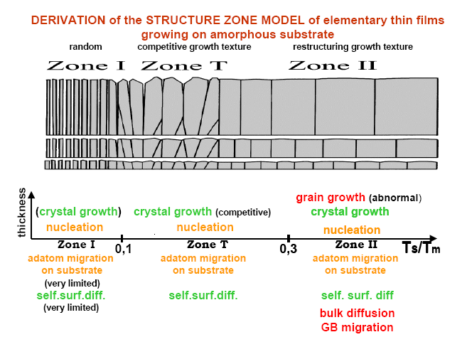
52 Ts is the deposition temperature and Tm is the melting point in K Conclusions on structure evolution in elemental thin films * correlation exists between grain size, grain morphology, surface topography and texture, these are developing together * the in-plane size (column diameter) and the orientation of crystals can be controlled by the temperature * the as-deposited structure has low thermal stability * the possible zones are: Zone I, Zone T and Zone II * in Zones I and II the structure and orientation are uniform along thickness, crystals penetrate through the film * no grain boundaries parallel to the substrate, i.e. no equiaxed grain morphology (Zone III ) can exist
53 PVD Structure Zone Models Movchan Demchishin T/T m : grain structure Thornton Inert gas pressure Messier Particle energy

54 Movchan-Demchishin: Evaporation Thornton: Sputtering
55 Conclusions (P.B. Barna, M. Adamik, Thin Solid Films, 317(1998)27; I. Petrov, P.B. Barna, L. Hultman, J.E. Greene, J. Vac. Sci. Technol.,21(2003)S117) The structure evolution in polycrystalline films (both elemental and multicomponent) can be described by a pathway (characteristic for every materials system) on the basis of the same fundamental phenomena of structure formation: nucleation, crystal growth, grain growth The operation of every single fundamental phenomenon is related to a thermally activated atomic process (temperature dependence of the pathway) The atomic processes are: adatom diffusion (Ts > ~ 0,05Tm) (nucleation) self surface diffusion (Ts > ~ 0,1Tm) (crystal growth, coalescence) bulk diffusion (Ts > ~ 0,3Tm) (grain growth) in multicomponent films additionally: chemical interaction among species including process induced segregation of excessive species resulting in delayed nucleation of secondary phase(s)
56 Acknowledgment Fully acknowledge the contribution of Alan Savan, CAESAR, Germany
Vacuum Evaporation Recap
 Sputtering Vacuum Evaporation Recap Use high temperatures at high vacuum to evaporate (eject) atoms or molecules off a material surface. Use ballistic flow to transport them to a substrate and deposit.
Coating Technology: Evaporation Vs Sputtering
 Satisloh Italy S.r.l. Coating Technology: Evaporation Vs Sputtering Gianni Monaco, PhD R&D project manager, Satisloh Italy 04.04.2016 V1 The aim of this document is to provide basic technical information
Lecture 12. Physical Vapor Deposition: Evaporation and Sputtering Reading: Chapter 12. ECE 6450 - Dr. Alan Doolittle
 Lecture 12 Physical Vapor Deposition: Evaporation and Sputtering Reading: Chapter 12 Evaporation and Sputtering (Metalization) Evaporation For all devices, there is a need to go from semiconductor to metal.
Deposition of Thin Metal Films " (on Polymer Substrates)!
!") Deposition of Thin Metal Films " (on Polymer Substrates)! Shefford P. Baker! Cornell University! Department of Materials Science and Engineering! Ithaca, New York, 14853! MS&E 5420 Flexible Electronics,
Deposition of Thin Metal Films " (on Polymer Substrates)! Shefford P. Baker! Cornell University! Department of Materials Science and Engineering! Ithaca, New York, 14853! MS&E 5420 Flexible Electronics,
2. Deposition process
 Properties of optical thin films produced by reactive low voltage ion plating (RLVIP) Antje Hallbauer Thin Film Technology Institute of Ion Physics & Applied Physics University of Innsbruck Investigations
Ion Beam Sputtering: Practical Applications to Electron Microscopy
 Ion Beam Sputtering: Practical Applications to Electron Microscopy Applications Laboratory Report Introduction Electron microscope specimens, both scanning (SEM) and transmission (TEM), often require a
Decorative vacuum coating technologies 30.05.2014 Certottica Longarone. Thin Film Plasma Coating Technologies
 Dr. Stefan Schlichtherle Dr. Georg Strauss PhysTech Coating Technology GmbH Decorative vacuum coating technologies 30.05.2014 Certottica Longarone Thin Film Plasma Coating Technologies Content The fascination
Types of Epitaxy. Homoepitaxy. Heteroepitaxy
 Epitaxy Epitaxial Growth Epitaxy means the growth of a single crystal film on top of a crystalline substrate. For most thin film applications (hard and soft coatings, optical coatings, protective coatings)
Chemical Sputtering. von Kohlenstoff durch Wasserstoff. W. Jacob
 Chemical Sputtering von Kohlenstoff durch Wasserstoff W. Jacob Centre for Interdisciplinary Plasma Science Max-Planck-Institut für Plasmaphysik, 85748 Garching Content: Definitions: Chemical erosion, physical
State of the art in reactive magnetron sputtering
 State of the art in reactive magnetron sputtering T. Nyberg, O. Kappertz, T. Kubart and S. Berg Solid State Electronics, The Ångström Laboratory, Uppsala University, Box 534, S-751 21 Uppsala, Sweden D.
Dry Etching and Reactive Ion Etching (RIE)
") Dry Etching and Reactive Ion Etching (RIE) MEMS 5611 Feb 19 th 2013 Shengkui Gao Contents refer slides from UC Berkeley, Georgia Tech., KU, etc. (see reference) 1 Contents Etching and its terminologies
Dry Etching and Reactive Ion Etching (RIE) MEMS 5611 Feb 19 th 2013 Shengkui Gao Contents refer slides from UC Berkeley, Georgia Tech., KU, etc. (see reference) 1 Contents Etching and its terminologies
Sputtering. Ion-Solid Interactions
 ssistant Professor Department of Microelectronic Engineering Rochester Institute of Technology 82 Lomb Memorial Drive Rochester, NY 14623-5604 Tel (716) 475-2923 Fax (716) 475-5041 PDRDV@RIT.EDU Page 1
THIN FILM MATERIALS TECHNOLOGY
 THIN FILM MATERIALS TECHNOLOGY Sputtering of Compound Materials by Kiyotaka Wasa Yokohama City University Yokohama, Japan Makoto Kitabatake Matsushita Electric Industrial Co., Ltd. Kyoto, Japan Hideaki
Electron Beam and Sputter Deposition Choosing Process Parameters
 Electron Beam and Sputter Deposition Choosing Process Parameters General Introduction The choice of process parameters for any process is determined not only by the physics and/or chemistry of the process,
For Touch Panel and LCD Sputtering/PECVD/ Wet Processing
 production Systems For Touch Panel and LCD Sputtering/PECVD/ Wet Processing Pilot and Production Systems Process Solutions with over 20 Years of Know-how Process Technology at a Glance for Touch Panel,
Reactive Sputtering Using a Dual-Anode Magnetron System
 Reactive Sputtering Using a Dual-Anode Magnetron System A. Belkind and Z. Zhao, Stevens Institute of Technology, Hoboken, NJ; and D. Carter, G. McDonough, G. Roche, and R. Scholl, Advanced Energy Industries,
OPTIMIZING OF THERMAL EVAPORATION PROCESS COMPARED TO MAGNETRON SPUTTERING FOR FABRICATION OF TITANIA QUANTUM DOTS
 OPTIMIZING OF THERMAL EVAPORATION PROCESS COMPARED TO MAGNETRON SPUTTERING FOR FABRICATION OF TITANIA QUANTUM DOTS Vojtěch SVATOŠ 1, Jana DRBOHLAVOVÁ 1, Marian MÁRIK 1, Jan PEKÁREK 1, Jana CHOMOCKÁ 1,
Introduction to VLSI Fabrication Technologies. Emanuele Baravelli
 Introduction to VLSI Fabrication Technologies Emanuele Baravelli 27/09/2005 Organization Materials Used in VLSI Fabrication VLSI Fabrication Technologies Overview of Fabrication Methods Device simulation
Module 7 Wet and Dry Etching. Class Notes
 Module 7 Wet and Dry Etching Class Notes 1. Introduction Etching techniques are commonly used in the fabrication processes of semiconductor devices to remove selected layers for the purposes of pattern
A Remote Plasma Sputter Process for High Rate Web Coating of Low Temperature Plastic Film with High Quality Thin Film Metals and Insulators
 A Remote Plasma Sputter Process for High Rate Web Coating of Low Temperature Plastic Film with High Quality Thin Film Metals and Insulators Dr Peter Hockley and Professor Mike Thwaites, Plasma Quest Limited
Conductivity of silicon can be changed several orders of magnitude by introducing impurity atoms in silicon crystal lattice.
 CMOS Processing Technology Silicon: a semiconductor with resistance between that of conductor and an insulator. Conductivity of silicon can be changed several orders of magnitude by introducing impurity
Microstockage d énergie Les dernières avancées. S. Martin (CEA-LITEN / LCMS Grenoble)
") Microstockage d énergie Les dernières avancées S. Martin (CEA-LITEN / LCMS Grenoble) 1 Outline What is a microbattery? Microbatteries developped at CEA Description Performances Integration and Demonstrations
Microstockage d énergie Les dernières avancées S. Martin (CEA-LITEN / LCMS Grenoble) 1 Outline What is a microbattery? Microbatteries developped at CEA Description Performances Integration and Demonstrations
Exploring the deposition of oxides on silicon for photovoltaic cells by pulsed laser deposition
 Applied Surface Science 186 2002) 453±457 Exploring the deposition of oxides on silicon for photovoltaic cells by pulsed laser deposition Lianne M. Doeswijk a,*, Hugo H.C. de Moor b, Horst Rogalla a, Dave
Sputtered AlN Thin Films on Si and Electrodes for MEMS Resonators: Relationship Between Surface Quality Microstructure and Film Properties
 Sputtered AlN Thin Films on and Electrodes for MEMS Resonators: Relationship Between Surface Quality Microstructure and Film Properties S. Mishin, D. R. Marx and B. Sylvia, Advanced Modular Sputtering,
Structure and properties of transparent conductive ZnO films grown by pulsed laser
 Structure and properties of transparent conductive ZnO films grown by pulsed laser deposition (PLD) by Yu Hsiu, Lin A dissertation submitted to the University of Birmingham for the degree of Master of
Tecnologie convenzionali nell approccio top-down; I: metodi e problematiche per la deposizione di film sottili
 LS Scienza dei Materiali - a.a. 2005/06 Fisica delle Nanotecnologie part 8 Version 4, Dec 2005 Francesco Fuso, tel 0502214305, 0502214293 - fuso@df.unipi.it http://www.df.unipi.it/~fuso/dida Tecnologie
Lectures about XRF (X-Ray Fluorescence)
") 1 / 38 Lectures about XRF (X-Ray Fluorescence) Advanced Physics Laboratory Laurea Magistrale in Fisica year 2013 - Camerino 2 / 38 X-ray Fluorescence XRF is an acronym for X-Ray Fluorescence. The XRF technique
1 / 38 Lectures about XRF (X-Ray Fluorescence) Advanced Physics Laboratory Laurea Magistrale in Fisica year 2013 - Camerino 2 / 38 X-ray Fluorescence XRF is an acronym for X-Ray Fluorescence. The XRF technique
Planar Magnetron Sputtering Sources
 Planar Magnetron puttering ources INTRODUCTION TABLE OF CONTENT PAGE Introduction........................ 2 MAK 1.3...........................3 MAK 2............................4 MAK 3............................5
Optical Properties of Sputtered Tantalum Nitride Films Determined by Spectroscopic Ellipsometry
 Optical Properties of Sputtered Tantalum Nitride Films Determined by Spectroscopic Ellipsometry Thomas Waechtler a, Bernd Gruska b, Sven Zimmermann a, Stefan E. Schulz a, Thomas Gessner a a Chemnitz University
Secondary Ion Mass Spectrometry
 Secondary Ion Mass Spectrometry A PRACTICAL HANDBOOK FOR DEPTH PROFILING AND BULK IMPURITY ANALYSIS R. G. Wilson Hughes Research Laboratories Malibu, California F. A. Stevie AT&T Bell Laboratories Allentown,
Lecture: 33. Solidification of Weld Metal
 Lecture: 33 Solidification of Weld Metal This chapter presents common solidification mechanisms observed in weld metal and different modes of solidification. Influence of welding speed and heat input on
1. Photon Beam Damage and Charging at Solid Surfaces John H. Thomas III
 1. Photon Beam Damage and Charging at Solid Surfaces John H. Thomas III 1. Introduction............................. 2. Electrostatic Charging of Samples in Photoemission Experiments............................
Chapter 5: Diffusion. 5.1 Steady-State Diffusion
 : Diffusion Diffusion: the movement of particles in a solid from an area of high concentration to an area of low concentration, resulting in the uniform distribution of the substance Diffusion is process
Cathodic Arc Deposition of superconducting thin films of MgB 2 for RF cavities*
 Alameda Applied Sciences Corporation Cathodic Arc Deposition of superconducting thin films of MgB 2 for RF cavities* Mahadevan Krishnan, Andrew Gerhan, Kristi Wilson and Brian Bures Alameda Applied Sciences
Surface Area and Porosity
 Surface Area and Porosity 1 Background Techniques Surface area Outline Total - physical adsorption External Porosity meso micro 2 Length 1 Å 1 nm 1 µm 1 1 1 1 1 mm macro meso micro metal crystallite 1-1
h e l p s y o u C O N T R O L
 contamination analysis for compound semiconductors ANALYTICAL SERVICES B u r i e d d e f e c t s, E v a n s A n a l y t i c a l g r o u p h e l p s y o u C O N T R O L C O N T A M I N A T I O N Contamination
Semiconductor doping. Si solar Cell
 Semiconductor doping Si solar Cell Two Levels of Masks - photoresist, alignment Etch and oxidation to isolate thermal oxide, deposited oxide, wet etching, dry etching, isolation schemes Doping - diffusion/ion
Introduction to Thin Film Technology LOT. Chair of Surface and Materials Technology
 Introduction to Thin Film Introduction to Thin Film Verfahrenstechnik der Oberflächenmodifikationen Prof. Dr. Xin Jiang Lecture Institut für Werkstofftechnik der Uni-Siegen Sommersemester 2007 Introduction
Graduate Student Presentations
 Graduate Student Presentations Dang, Huong Chip packaging March 27 Call, Nathan Thin film transistors/ liquid crystal displays April 4 Feldman, Ari Optical computing April 11 Guerassio, Ian Self-assembly
NANOSTRUCTURED ZnO AND ZAO TRANSPARENT THIN FILMS BY SPUTTERING SURFACE CHARACTERIZATION
 Rev.Adv.Mater.Sci. Nanostructured ZnO 10 and (2005) ZAO 335-340 transparent thin films by sputtering surface characterization 335 NANOSTRUCTURED ZnO AND ZAO TRANSPARENT THIN FILMS BY SPUTTERING SURFACE
BAL-TEC SCD 005. Scientist in charge: Lhoussaine Belkoura 07/14/06. softcomp soft matter composites 1
 07/14/06 softcomp soft matter composites 1 BAL-TEC SCD 005 Institution: University of Cologne Scientist in charge: Lhoussaine Belkoura SCD 005 Cool Sputter Coater 26.02.99 Internet: www.bal-tec.com & 1
Pulsed laser deposition of organic materials
 Pulsed laser deposition of organic materials PhD theses Gabriella Kecskeméti Department of Optics and Quantum Electronics University of Szeged Supervisor: Dr. Béla Hopp senior research fellow Department
Neuere Entwicklungen zur Herstellung optischer Schichten durch reaktive. Wolfgang Hentsch, Dr. Reinhard Fendler. FHR Anlagenbau GmbH
 Neuere Entwicklungen zur Herstellung optischer Schichten durch reaktive Sputtertechnologien Wolfgang Hentsch, Dr. Reinhard Fendler FHR Anlagenbau GmbH Germany Contents: 1. FHR Anlagenbau GmbH in Brief
Plasma Electronic is Partner of. Tailor-Made Surfaces by Plasma Technology
 Precision Fair 2013 Stand 171 Plasma Electronic is Partner of Tailor-Made Surfaces by Plasma Technology Dr. J. Geng, Plasma Electronic GmbH Modern Surface Technology in 1900 Overview A short introduction
NANO SILICON DOTS EMBEDDED SIO 2 /SIO 2 MULTILAYERS FOR PV HIGH EFFICIENCY APPLICATION
 NANO SILICON DOTS EMBEDDED SIO 2 /SIO 2 MULTILAYERS FOR PV HIGH EFFICIENCY APPLICATION Olivier Palais, Damien Barakel, David Maestre, Fabrice Gourbilleau and Marcel Pasquinelli 1 Outline Photovoltaic today
Plasma Source. Atom Source, Ion Source and Atom/Ion Hybrid Source
 Plasma Source Atom Source, Ion Source and Atom/Ion Hybrid Source The tectra Plasma Source* is a multi-purpose source which can easily be user configured to produce either atoms or ions and finds uses in
Surface characterization of oxygen deficient SrTiO 3
 U. Scotti di Uccio Surface characterization of oxygen deficient SrTiO 3 films and single crystals Coherentia-CNR-INFM Napoli, Italy Prof. R. Vaglio R. Di Capua, G. De Luca, M. Radovic, N. Lampis, P. Perna,
Principles of Ion Implant
 Principles of Ion Implant Generation of ions dopant gas containing desired species BF 3, B 2 H 6, PH 3, AsH 3, AsF 5 plasma provides positive ions (B 11 ) +, BF 2+, (P 31 ) +, (P 31 ) ++ Ion Extraction
2. Nanoparticles. Introduction to Nanoscience, 2005 1
 2. Nanoparticles Nanoparticles are the simplest form of structures with sizes in the nm range. In principle any collection of atoms bonded together with a structural radius of < 100 nm can be considered
Al 2 O 3, Its Different Molecular Structures, Atomic Layer Deposition, and Dielectrics
 Al 2 O 3, Its Different Molecular Structures, Atomic Layer Deposition, and Dielectrics Mark Imus Douglas Sisk, Ph.D., Mentor Marian High School RET Program University of Notre Dame Project Proposal Tunneling
Dependence of the thickness and composition of the HfO 2 /Si interface layer on annealing
 Dependence of the thickness and composition of the HfO 2 /Si interface layer on annealing CINVESTAV-UNIDAD QUERETARO P.G. Mani-González and A. Herrera-Gomez gmani@qro.cinvestav.mx CINVESTAV 1 background
Improved Contact Formation for Large Area Solar Cells Using the Alternative Seed Layer (ASL) Process
 Process") Improved Contact Formation for Large Area Solar Cells Using the Alternative Seed Layer (ASL) Process Lynne Michaelson, Krystal Munoz, Jonathan C. Wang, Y.A. Xi*, Tom Tyson, Anthony Gallegos Technic Inc.,
Improved Contact Formation for Large Area Solar Cells Using the Alternative Seed Layer (ASL) Process Lynne Michaelson, Krystal Munoz, Jonathan C. Wang, Y.A. Xi*, Tom Tyson, Anthony Gallegos Technic Inc.,
Lecture 11. Etching Techniques Reading: Chapter 11. ECE 6450 - Dr. Alan Doolittle
 Lecture 11 Etching Techniques Reading: Chapter 11 Etching Techniques Characterized by: 1.) Etch rate (A/minute) 2.) Selectivity: S=etch rate material 1 / etch rate material 2 is said to have a selectivity
High Rate Oxide Deposition onto Web by Reactive Sputtering from Rotatable Magnetrons
 High Rate Oxide Deposition onto Web by Reactive Sputtering from Rotatable Magnetrons D.Monaghan, V. Bellido-Gonzalez, M. Audronis. B. Daniel Gencoa, Physics Rd, Liverpool, L24 9HP, UK. www.gencoa.com,
Physical Properties and Functionalization of Low-Dimensional Materials
 Physical Properties and Functionalization of Low-Dimensional Materials Physics Department, University of Trieste Graduate School of Physics, XXVI cycle Supervisor: Co-supervisor: Prof. Alessandro BARALDI
Etudes in situ et ex situ de multicouches C/FePt
 Etudes in situ et ex situ de multicouches C/FePt : influence de la température sur la structure et les propriétés s magnétiques D. Babonneau, G. Abadias, F. Pailloux Laboratoire de Physique des Matériaux
How To Make A Plasma Control System
 XXII. Erfahrungsaustausch Mühlleiten 2015 Plasmaanalyse und Prozessoptimierung mittels spektroskopischem Plasmamonitoring in industriellen Anwendungen Swen Marke,, Lichtenau Thomas Schütte, Plasus GmbH,
How do single crystals differ from polycrystalline samples? Why would one go to the effort of growing a single crystal?
 Crystal Growth How do single crystals differ from polycrystalline samples? Single crystal specimens maintain translational symmetry over macroscopic distances (crystal dimensions are typically 0.1 mm 10
Luminescence study of structural changes induced by laser cutting in diamond films
 Luminescence study of structural changes induced by laser cutting in diamond films A. Cremades and J. Piqueras Departamento de Fisica de Materiales, Facultad de Fisicas, Universidad Complutense, 28040
Modification of Pd-H 2 and Pd-D 2 thin films processed by He-Ne laser
 Modification of Pd-H 2 and Pd-D 2 thin films processed by He-Ne laser V.Nassisi #, G.Caretto #, A. Lorusso #, D.Manno %, L.Famà %, G.Buccolieri %, A.Buccolieri %, U.Mastromatteo* # Laboratory of Applied
Production of Solar Energy Using Nanosemiconductors
 Production of Solar Energy Using Nanosemiconductors 1 Kiruthika S, 2 Dinesh Kumar M, 3 Surendar.A 1, 2 II year, KSR College of Engineering, Tiruchengode, Tamilnadu, India 3 Assistant Professor, KSR College
Sputtering by Particle Bombardment I
 Sputtering by Particle Bombardment I Physical Sputtering of Single-Element Solids Edited by R. Behrisch With Contributions by H. H. Andersen H. L. Bay R. Behrisch M. T. Robinson H. E. Roosendaal P. Sigmund
III. Wet and Dry Etching
 III. Wet and Dry Etching Method Environment and Equipment Advantage Disadvantage Directionality Wet Chemical Solutions Atmosphere, Bath 1) Low cost, easy to implement 2) High etching rate 3) Good selectivity
Sputter deposition processes
 Sputter deposition processes D. Depla 1, S. Mahieu 1, J.E. Greene 2 1 Ghent University, Department of Solid State Sciences, Krijgslaan 281 (S1), 9000 Ghent, Belgium 2 Materials Science and Physics Departments
How MOCVD. Works Deposition Technology for Beginners
 How MOCVD Works Deposition Technology for Beginners Contents MOCVD for Beginners...3 MOCVD A Definition...4 Planetary Reactor Technology...5 Close Coupled Showerhead Technology...6 AIXTRON MOCVD Production
OLED display. Ying Cao
 OLED display Ying Cao Outline OLED basics OLED display A novel method of fabrication of flexible OLED display Potentials of OLED Suitable for thin, lightweight, printable displays Broad color range Good
Formation of solids from solutions and melts
 Formation of solids from solutions and melts Solids from a liquid phase. 1. The liquid has the same composition as the solid. Formed from the melt without any chemical transformation. Crystallization and
View of ΣIGMA TM (Ref. 1)
") Overview of the FESEM system 1. Electron optical column 2. Specimen chamber 3. EDS detector [Electron Dispersive Spectroscopy] 4. Monitors 5. BSD (Back scatter detector) 6. Personal Computer 7. ON/STANDBY/OFF
Overview of the FESEM system 1. Electron optical column 2. Specimen chamber 3. EDS detector [Electron Dispersive Spectroscopy] 4. Monitors 5. BSD (Back scatter detector) 6. Personal Computer 7. ON/STANDBY/OFF
Study on the early stage of thin filmgrowth in pulsed beamdeposition by kinetic Monte Carlo simulation
 Surface and Coatings Technology 158 159 (2002) 247 252 Study on the early stage of thin filmgrowth in pulsed beamdeposition by kinetic Monte Carlo simulation a, b Q.Y. Zhang *, P.K. Chu a State Key Laboratory
BNG 331 Cell-Tissue Material Interactions. Biomaterial Surfaces
 BNG 331 Cell-Tissue Material Interactions Biomaterial Surfaces Course update Updated syllabus Homework 4 due today LBL 5 Friday Schedule for today: Chapter 8 Biomaterial surface characterization Surface
Solid State Detectors = Semi-Conductor based Detectors
 Solid State Detectors = Semi-Conductor based Detectors Materials and their properties Energy bands and electronic structure Charge transport and conductivity Boundaries: the p-n junction Charge collection
Plasma Cleaner: Physics of Plasma
 Plasma Cleaner: Physics of Plasma Nature of Plasma A plasma is a partially ionized gas consisting of electrons, ions and neutral atoms or molecules The plasma electrons are at a much higher temperatures
Short overview of TEUFEL-project
 Short overview of TEUFEL-project ELAN-meeting may 2004 Frascati (I) Contents Overview of TEUFEL project at Twente Photo cathode research Recent experience Outlook Overview FEL Drive laser Photo cathode
Chapter 4 Indium Tin Oxide Films Deposited by d.c. Sputtering
 Chapter 4 Indium Tin Oxide Films Deposited by d.c. Sputtering 4.1. Introduction Indium-tin-oxide (ITO) thin films are widely used in optoelectronics devices, flat panel display and electrochromic (EC)
EXPERIMENTAL STUDY OF STRUCTURAL ZONE MODEL FOR COMPOSITE THIN FILMS IN MAGNETIC RECORDING MEDIA APPLICATION
 EXPERIMENTAL STUDY OF STRUCTURAL ZONE MODEL FOR COMPOSITE THIN FILMS IN MAGNETIC RECORDING MEDIA APPLICATION Hua Yuan and David E. Laughlin Department of Materials Science and Engineering, Carnegie Mellon
Chapter 7-1. Definition of ALD
 Chapter 7-1 Atomic Layer Deposition (ALD) Definition of ALD Brief history of ALD ALD process and equipments ALD applications 1 Definition of ALD ALD is a method of applying thin films to various substrates
7. advanced SEM. Latest generation of SEM SEM
 7. advanced SEM SEM Low voltage SE imaging Condition of the surface, coatings, plasma cleaning Low voltage BSE imaging Polishing for BSE, EDX and EBSD, effect of ion beam etching/polishing 1 Latest generation
Defects Introduction. Bonding + Structure + Defects. Properties
 Defects Introduction Bonding + Structure + Defects Properties The processing determines the defects Composition Bonding type Structure of Crystalline Processing factors Defects Microstructure Types of
Amorphous Transparent Conducting Oxides (TCOs) Deposited at T 100 C
 Deposited at T 100 C") Amorphous Transparent Conducting Oxides (TCOs) Deposited at T 100 C John Perkins, Maikel van Hest, Charles Teplin, Jeff Alleman, Matthew Dabney, Lynn Gedvilas, Brian Keyes, Bobby To, David Ginley National
Amorphous Transparent Conducting Oxides (TCOs) Deposited at T 100 C John Perkins, Maikel van Hest, Charles Teplin, Jeff Alleman, Matthew Dabney, Lynn Gedvilas, Brian Keyes, Bobby To, David Ginley National
Keywords: Planar waveguides, sol-gel technology, transmission electron microscopy
 Structural and optical characterisation of planar waveguides obtained via Sol-Gel F. Rey-García, C. Gómez-Reino, M.T. Flores-Arias, G.F. De La Fuente, W. Assenmacher, W. Mader ABSTRACT Planar waveguides
Dr Marcin Adamiak marcin.adamiak. www.imiib.polsl.pl/
 FP7 NMP/INCO Brokerage Event Warsaw, 17-18 September 2009 Dr Marcin Adamiak marcin.adamiak adamiak@polsl.pl http://www.imiib.polsl.pl www.imiib.polsl.pl/ Institute of Engineering Materials and Biomaterials
Methods of plasma generation and plasma sources
 Methods of plasma generation and plasma sources PlasTEP trainings course and Summer school 2011 Warsaw/Szczecin Indrek Jõgi, University of Tartu Partfinanced by the European Union (European Regional Development
Microstockage d énergie Les dernières avancées. S. Martin (CEA-LITEN / Grenoble)
") Microstockage d énergie Les dernières avancées S. Martin (CEA-LITEN / Grenoble) 1 Outline What is a microbattery? Microbatteries developped at CEA Description Performances Integration and Demonstrations
Microstockage d énergie Les dernières avancées S. Martin (CEA-LITEN / Grenoble) 1 Outline What is a microbattery? Microbatteries developped at CEA Description Performances Integration and Demonstrations
The study of structural and optical properties of TiO 2 :Tb thin films
 Optica Applicata, Vol. XXXVII, No. 4, 2007 The study of structural and optical properties of TiO 2 :Tb thin films AGNIESZKA BORKOWSKA, JAROSLAW DOMARADZKI, DANUTA KACZMAREK, DAMIAN WOJCIESZAK Faculty of
Impurity-doped ZnO Thin Films Prepared by Physical Deposition Methods Appropriate for
 Home Search Collections Journals About Contact us My IOPscience Impurity-doped ZnO Thin Films Prepared by Physical Deposition Methods Appropriate for Transparent Electrode Applications in Thin-film Solar
Laser beam sintering of coatings and structures
 Laser beam sintering of coatings and structures Anne- Maria Reinecke, Peter Regenfuß, Maren Nieher, Sascha Klötzer, Robby Ebert, Horst Exner Laserinstitut Mittelsachsen e.v. an der Hochschule Mittweida,
HPPMS/DC-MSIP (Cr,Al,V)N and (Cr,Al,W)N Thin Films for High Temperature Application
N and (Cr,Al,W)N Thin Films for High Temperature Application") HPPMS/DC-MSIP (Cr,Al,V)N and (Cr,Al,W)N Thin Films for High Temperature Application Sebastian Theiß K. Bobzin, N. Bagcivan, M. Ewering, R. H. Brugnara April 23, 21 HPPMS/HiPIMS/MPP Workshop, Golden Outline
HPPMS/DC-MSIP (Cr,Al,V)N and (Cr,Al,W)N Thin Films for High Temperature Application Sebastian Theiß K. Bobzin, N. Bagcivan, M. Ewering, R. H. Brugnara April 23, 21 HPPMS/HiPIMS/MPP Workshop, Golden Outline
1. PECVD in ORGANOSILICON FED PLASMAS
 F. FRACASSI Department of Chemistry, University of Bari (Italy) Plasma Solution srl SURFACE MODIFICATION OF POLYMERS AND METALS WITH LOW TEMPERATURE PLASMA OUTLINE METAL TREATMENTS 1 low pressure PECVD
METHODS FOR PULSED LASER DEPOSITION OF LARGE-AREA FILMS USING MORE THAN ONE TARGET
 Laser Physics 0 International Journal of Modern Physics: Conference Series Vol. 5 (0) 70 78 World Scientific Publishing Company DOI: 0.4/S009450078 METHODS FOR PULSED LASER DEPOSITION OF LARGE-AREA FILMS
Solar Photovoltaic (PV) Cells
 Cells") Solar Photovoltaic (PV) Cells A supplement topic to: Mi ti l S Micro-optical Sensors - A MEMS for electric power generation Science of Silicon PV Cells Scientific base for solar PV electric power generation
Solar Photovoltaic (PV) Cells A supplement topic to: Mi ti l S Micro-optical Sensors - A MEMS for electric power generation Science of Silicon PV Cells Scientific base for solar PV electric power generation
Modern Construction Materials Prof. Ravindra Gettu Department of Civil Engineering Indian Institute of Technology, Madras
 Modern Construction Materials Prof. Ravindra Gettu Department of Civil Engineering Indian Institute of Technology, Madras Module - 2 Lecture - 2 Part 2 of 2 Review of Atomic Bonding II We will continue
Chapter 12 - Liquids and Solids
 Chapter 12 - Liquids and Solids 12-1 Liquids I. Properties of Liquids and the Kinetic Molecular Theory A. Fluids 1. Substances that can flow and therefore take the shape of their container B. Relative
In the previous presentation, we discussed how x-rays were discovered and how they are generated at the atomic level. Today we will begin the
 In the previous presentation, we discussed how x-rays were discovered and how they are generated at the atomic level. Today we will begin the discussion on the major components of the x-ray machine. Today
histaris Inline Sputtering Systems
 vistaris histaris Inline Sputtering Systems Inline Sputtering Systems with Vertical Substrate Transport Modular System for Different Applications VISTARIS Sputtering Systems The system with the brand name
Molecular Beam Epitaxy
 Molecular Beam Epitaxy Klaus Ploog Paul Drude Institut Tutorial Session #1 Epitaxial Growth 27 th International Conference on the Physics of Semiconductors Flagstaff, AZ, 2004 Molecular Beam Epitaxy (MBE)
 Chapter 6 Atmospheric Aerosol and Cloud Processes Spring 2015 Cloud Physics Initiation and development of cloud droplets Special interest: Explain how droplet formation results in rain in approximately
TOF FUNDAMENTALS TUTORIAL
 TOF FUNDAMENTALS TUTORIAL Presented By: JORDAN TOF PRODUCTS, INC. 990 Golden Gate Terrace Grass Valley, CA 95945 530-272-4580 / 530-272-2955 [fax] www.rmjordan.com [web] info@rmjordan.com [e-mail] This
Handbook of Thin Film Materials
 Handbook of Thin Film Materials Volume 1 Deposition and Processing of Thin Films Edited by Hari Singh Nalwa, M.Sc, Ph.D. Stanford Scientific Corporation Los Angeles, California, USA Formerly at Hitachi
Plasma diagnostics focused on new magnetron sputtering devices for thin film deposition
 Université Paris-Sud XI Laboratoire de Physique des Gaz et des Plasmas Orsay, France & Masaryk University in Brno Department of Physical Electronics Brno, Czech Republic Plasma diagnostics focused on new
Chapter 11 PVD and Metallization
 Chapter 11 PVD and Metallization 2006/5/23 1 Metallization Processes that deposit metal thin film on wafer surface. 2006/5/23 2 1 Metallization Definition Applications PVD vs. CVD Methods Vacuum Metals