Experiment 2: AC and DC Transistor Gain. For more courses visit
|
|
|
- Andra Potter
- 7 years ago
- Views:
Transcription
1 Experiment 2: AC and DC Transistor Gain For more courses visit
2 1. To show how to determine the AC and DC current gain values of a transistor from its characteristics curves 2. To give more experience plotting characteristic curves 3. To demonstrate the characteristics among various transistors of the same type can vary considerably
3 Previously, you learned to plot the common-emitter characteristics of a typical NPN transistor. As part of this experiment, you will plot two other sets of curves, to show the characteristics vary among transistors of the same type
4 You will also learn to determine transistor gain by merely picking out appropriate points on a graph and doing some simple calculations. The D-C current gain of a transistor is simply the collector current divided by the base current. β D C = I C I B The Greek letter β (Beta) represents the current gain which is also represented as h FE
5 The current gain can be determined by picking V CE and I B values from the characteristic curves and then reading the collector current Example: Look at the following (A-C and D-C Current Gain Calculation Graph); when VCE = 5.5 V and IB = 30 ma, the collector current is 6 ma. The D-C beta is: β D-C = 6 x x 10 6 = 200
6
7 Note: The actual values of β will depend somewhat on the point on the graph. The curves shown in this case are for an ideal transistor, so that almost any point we pick will give us the same beta Expect some real world variations when completing the experiment, since practical transistors are always less than perfect
8 The a-c current gain calculation differs from the d-c current gain calculation. The a-c gain is calculated in terms of specific increments of base current This technique give a more accurate picture of how a transistor reacts to a-c signals
9 Use the previous graph (A-C and D-C Current Gain Calculation Graph) to determine the A-C current gain Determine how the collector current changes when the base current is varied between 20 µa and 40 µa with V CE held constant at 5 V Use the following formula to determine the A-C Current Gain. β A C = ΔI C The Δ (delta) symbol means ΔI B change in
10 Using the values from our current a-c example, we have: β A C = 8 x 10 3 (4 x 10 3 ) = 4 x x 10 6 (20 x 10 6 ) 200 x 10 6 = 200 The A-C current is sometimes call h fe & is the same as the D-C gain in this case, since we are using ideal characteristics. We usually expect a considerable difference in values with practical transistors, but the A-C and D-C values may be the same
11 Please note! The current gains we have been discussing are for the transistor itself, not the amplifier circuit. Biasing networks, input, output and loading will usually decrease the current gain of a practical CE amplifier You will plot the characteristics of two more transistors, then compare the results with the curves you obtained from the first experiment s transistor
12 Finally, you will calculate the AC and DC gains for all three transistors. You should see that generally speaking, no two transistors are entirely alike. Matched sets are available for special purchase
 Note: Your results may be considerably different than those found by CIE. This is because the current gain for each transistor may be quite different.")
13 1 330 W, ½ Watt Resistor (orange, orange, brown) kw, ½ Watt Resistor (brown, black, yellow) 1 1 kw potentiometer (on trainer) kw potentiometer (on trainer) 1 MPSA20 NPN transistor (or similar) Note: Your results may be considerably different than those found by CIE. This is because the current gain for each transistor may be quite different. Do not be surprised if your results are not close to ours.
14 The circuit for this experiment (Exp. 2) is the same circuit as you built in Exp. 1. You will be measuring the characteristics of two more MPSA20 transistors and then compare the data with the characteristics of the MPSA20 transistor used in the first experiment. (1432 Exp. 1)
15 1. Locate the MPSA20 transistor used in 1432 Exp. 1 and set it aside for future use. Mark this transistor as Q1 a) Find two more MPSA20 transistors and mark them Q2 and Q3, so you will be able to identify them later 2. Construct the circuit on the following slide and use the transistor that you marked as Q2 a) Connect the transistors properly
16
17
18 1. Transistors wired incorrectly is a common mistake 3. Measure the collector current values for Q2 using the given base currents and VCE setting a) Mark the measured values in the data table for transistors Q2 characteristics on the next slide
19
20 4. Complete all the readings for Q2 and then replace the transistor with Q3 as demonstrated in the following schematic diagram a) Repeat the measurements for Q3 and then turn off the power supply.
21
22
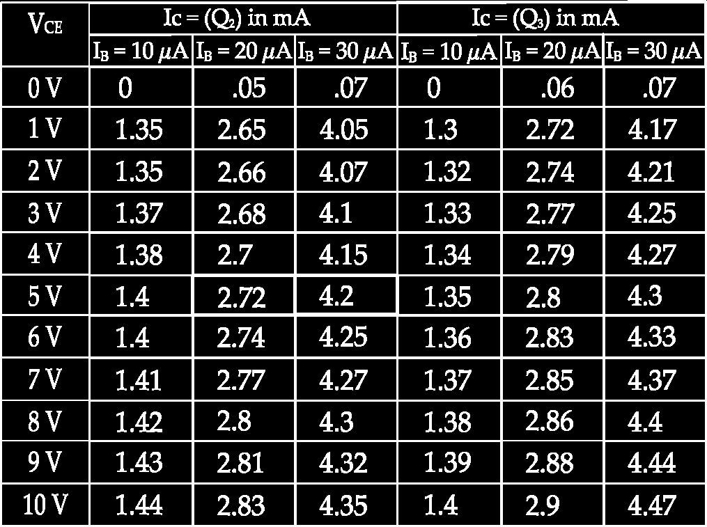
23 5. Plot the data points for Q2 on the Q2 Characteristic Curve Graph. a) Plot the data points for Q2 on the Q2 Characteristic Curve Graph. b) Connect each set of data points and draw smooth lines for each set after all the data has been plotted.
24
25
26 6. Compare your curves with the one you developed from the first experiment. Are the three family of curves identical? This means the three family of curves (do)(don t) have identical characteristics. 7. You can now see how the DC and AC gains differ, since you have completed the sets/families of characteristic curves for the three transistors.
27 a) Now, based on the three transistor curves, determine the value of I C when I B = 20 µa and V CE = 5 V. b) Record each value of I C in line 1 of the Data Table for Current Gain Calculations, under the appropriate heading 8. We can calculate the DC gain, with IB equaling 20 µa.
28 a) Use the following formula to calculate for β DC for each transistor 1. β DC = I C 20 x Calculate each DC current gain value, and enter it in line 2 of the Current Gain Calculations Data Table 10. The AC current gain is calculated by finding out how much the collector current varies when the base current changes by a certain amount
29 a) We will use a base current of ±10 μa for this experiment. Use the graphs for all three transistors as you did previously and record the values in line 3 of the Current Gain Calculations Data Table 11. Now find the value of I C for all three transistors at a base current of 30 µa and a V CE of 5 V. a) Record the value for each transistor in line 4 of the data table
30 12. The AC current gain of each transistor may be found using the following formula: βac = I C I B a) In this case, ΔI B is 20 µa (30 10 µa), while ΔI C is the difference between line 4 and line 3 of the Current Gain Calculation Data Table b) Record the results of the calculations in the Current Gain Calculation Data Table

31 Our results can be seen on the following four slides. Considerable variation can be expected due to the wide variations of transistor gain. Do not let the variation worry you as long as you show the same general pattern we do.
32
33
34
35
36
37 6. No: don t Of course it is possible for two samples of the same transistor type to have the same characteristics. However, such a possibility is very slight 13. Don t See the Current Gain Calculations Data Table 14. Don t See the I Gain Calc. Data Table
38 In this experiment, you measured the characteristics of two MPSA 20 transistors. Using the family of characteristic curves obtained from these two transistors along with the family of curves from the transistor in experiment 1, you were able to make direct comparisons of the characteristics of a total of 3 transistors
39 You were also able to use the curves to calculate the AC and DC current gains and see how the compared You probably obtained different characteristics for each of the three MPSA20 transistors. Although, it is possible, just barely, that the characteristics of two transistors were exactly the same
40 However, it is far more likely, the differences of the three transistors were readily apparent. This allowed you to see the extreme variability that can be expected in the characteristics of such solid state devices The current gain calculations for all three devices should have been somewhat different as well.
41 Again, the probability of identical gain characteristics is remote. The stated tolerance for the current gain of an MPSA20 transistor is in the range of


42
43 Rosenow, K. (2001). Lesson 1432: Common-Emitter Amplifier Characteristics. Cleveland: Cleveland Institute of Electronics.
44 Developed and Produced by the Instructors in the CIE Instruction Department. Copyright 12/2012 All Rights Reserved / Dec. 2012
LAB VII. BIPOLAR JUNCTION TRANSISTOR CHARACTERISTICS
 LAB VII. BIPOLAR JUNCTION TRANSISTOR CHARACTERISTICS 1. OBJECTIVE In this lab, you will study the DC characteristics of a Bipolar Junction Transistor (BJT). 2. OVERVIEW You need to first identify the physical
LAB VIII. BIPOLAR JUNCTION TRANSISTOR CHARACTERISTICS
 LAB VIII. BIPOLAR JUNCTION TRANSISTOR CHARACTERISTICS 1. OBJECTIVE In this lab, you will study the DC characteristics of a Bipolar Junction Transistor (BJT). 2. OVERVIEW In this lab, you will inspect the
BJT Characteristics and Amplifiers
 BJT Characteristics and Amplifiers Matthew Beckler beck0778@umn.edu EE2002 Lab Section 003 April 2, 2006 Abstract As a basic component in amplifier design, the properties of the Bipolar Junction Transistor
Bipolar Junction Transistor Basics
 by Kenneth A. Kuhn Sept. 29, 2001, rev 1 Introduction A bipolar junction transistor (BJT) is a three layer semiconductor device with either NPN or PNP construction. Both constructions have the identical
LABORATORY 2 THE DIFFERENTIAL AMPLIFIER
 LABORATORY 2 THE DIFFERENTIAL AMPLIFIER OBJECTIVES 1. To understand how to amplify weak (small) signals in the presence of noise. 1. To understand how a differential amplifier rejects noise and common
Basic Electronics Prof. Dr. Chitralekha Mahanta Department of Electronics and Communication Engineering Indian Institute of Technology, Guwahati
 Basic Electronics Prof. Dr. Chitralekha Mahanta Department of Electronics and Communication Engineering Indian Institute of Technology, Guwahati Module: 2 Bipolar Junction Transistors Lecture-2 Transistor
University of California, Berkeley Department of Electrical Engineering and Computer Sciences EE 105: Microelectronic Devices and Circuits
 University of California, Berkeley Department of Electrical Engineering and Computer Sciences EE 105: Microelectronic Devices and Circuits LTSpice LTSpice is a free circuit simulator based on Berkeley
Electronics. Discrete assembly of an operational amplifier as a transistor circuit. LD Physics Leaflets P4.2.1.1
 Electronics Operational Amplifier Internal design of an operational amplifier LD Physics Leaflets Discrete assembly of an operational amplifier as a transistor circuit P4.2.1.1 Objects of the experiment
Transistor Characteristics and Single Transistor Amplifier Sept. 8, 1997
 Physics 623 Transistor Characteristics and Single Transistor Amplifier Sept. 8, 1997 1 Purpose To measure and understand the common emitter transistor characteristic curves. To use the base current gain
Transistors. NPN Bipolar Junction Transistor
 Transistors They are unidirectional current carrying devices with capability to control the current flowing through them The switch current can be controlled by either current or voltage ipolar Junction
Physics 623 Transistor Characteristics and Single Transistor Amplifier Sept. 13, 2006
 Physics 623 Transistor Characteristics and Single Transistor Amplifier Sept. 13, 2006 1 Purpose To measure and understand the common emitter transistor characteristic curves. To use the base current gain
The 2N3393 Bipolar Junction Transistor
 The 2N3393 Bipolar Junction Transistor Common-Emitter Amplifier Aaron Prust Abstract The bipolar junction transistor (BJT) is a non-linear electronic device which can be used for amplification and switching.
AMPLIFIERS BJT BJT TRANSISTOR. Types of BJT BJT. devices that increase the voltage, current, or power level
 AMPLFERS Prepared by Engr. JP Timola Reference: Electronic Devices by Floyd devices that increase the voltage, current, or power level have at least three terminals with one controlling the flow between
MAS.836 HOW TO BIAS AN OP-AMP
 MAS.836 HOW TO BIAS AN OP-AMP Op-Amp Circuits: Bias, in an electronic circuit, describes the steady state operating characteristics with no signal being applied. In an op-amp circuit, the operating characteristic
Transistor Amplifiers
 Physics 3330 Experiment #7 Fall 1999 Transistor Amplifiers Purpose The aim of this experiment is to develop a bipolar transistor amplifier with a voltage gain of minus 25. The amplifier must accept input
Bipolar Junction Transistors
 Bipolar Junction Transistors Physical Structure & Symbols NPN Emitter (E) n-type Emitter region p-type Base region n-type Collector region Collector (C) B C Emitter-base junction (EBJ) Base (B) (a) Collector-base
Series and Parallel Circuits
 Direct Current (DC) Direct current (DC) is the unidirectional flow of electric charge. The term DC is used to refer to power systems that use refer to the constant (not changing with time), mean (average)
CONSTRUCTING A VARIABLE POWER SUPPLY UNIT
 CONSTRUCTING A VARIABLE POWER SUPPLY UNIT Building a power supply is a good way to put into practice many of the ideas we have been studying about electrical power so far. Most often, power supplies are
Objectives The purpose of this lab is build and analyze Differential amplifiers based on NPN transistors (or NMOS transistors).
.") 1 Lab 03: Differential Amplifiers (BJT) (20 points) NOTE: 1) Please use the basic current mirror from Lab01 for the second part of the lab (Fig. 3). 2) You can use the same chip as the basic current mirror;
1 Lab 03: Differential Amplifiers (BJT) (20 points) NOTE: 1) Please use the basic current mirror from Lab01 for the second part of the lab (Fig. 3). 2) You can use the same chip as the basic current mirror;
Bipolar Transistor Amplifiers
 Physics 3330 Experiment #7 Fall 2005 Bipolar Transistor Amplifiers Purpose The aim of this experiment is to construct a bipolar transistor amplifier with a voltage gain of minus 25. The amplifier must
POWER SUPPLY MODEL XP-15. Instruction Manual ELENCO
 POWER SUPPLY MODEL XP-15 Instruction Manual ELENCO Copyright 2013 by Elenco Electronics, Inc. REV-A 753020 All rights reserved. No part of this book shall be reproduced by any means; electronic, photocopying,
TRANSISTOR/DIODE TESTER
 TRANSISTOR/DIODE TESTER MODEL DT-100 Lesson Manual ELENCO Copyright 2012, 1988 REV-G 753115 Elenco Electronics, Inc. Revised 2012 FEATURES Diode Mode: 1. Checks all types of diodes - germanium, silicon,
Unit/Standard Number. High School Graduation Years 2010, 2011 and 2012
 1 Secondary Task List 100 SAFETY 101 Demonstrate an understanding of State and School safety regulations. 102 Practice safety techniques for electronics work. 103 Demonstrate an understanding of proper
Chapter 19 Operational Amplifiers
 Chapter 19 Operational Amplifiers The operational amplifier, or op-amp, is a basic building block of modern electronics. Op-amps date back to the early days of vacuum tubes, but they only became common
Building the AMP Amplifier
 Building the AMP Amplifier Introduction For about 80 years it has been possible to amplify voltage differences and to increase the associated power, first with vacuum tubes using electrons from a hot filament;
W04 Transistors and Applications. Yrd. Doç. Dr. Aytaç Gören
 W04 Transistors and Applications W04 Transistors and Applications ELK 2018 - Contents W01 Basic Concepts in Electronics W02 AC to DC Conversion W03 Analysis of DC Circuits (self and condenser) W04 Transistors
Transistor Biasing. The basic function of transistor is to do amplification. Principles of Electronics
 192 9 Principles of Electronics Transistor Biasing 91 Faithful Amplification 92 Transistor Biasing 93 Inherent Variations of Transistor Parameters 94 Stabilisation 95 Essentials of a Transistor Biasing
Voltage Divider Bias
 Voltage Divider Bias ENGI 242 ELEC 222 BJT Biasing 3 For the Voltage Divider Bias Configurations Draw Equivalent Input circuit Draw Equivalent Output circuit Write necessary KVL and KCL Equations Determine
11: AUDIO AMPLIFIER I. INTRODUCTION
 11: AUDIO AMPLIFIER I. INTRODUCTION The properties of an amplifying circuit using an op-amp depend primarily on the characteristics of the feedback network rather than on those of the op-amp itself. A
Differential Amplifier Offset. Causes of dc voltage and current offset Modeling dc offset R C
 ESE39 ntroduction to Microelectronics Differential Amplifier Offset Causes of dc voltage and current offset Modeling dc offset mismatch S mismatch β mismatch transistor mismatch dc offsets in differential
Amplifier Teaching Aid
 Amplifier Teaching Aid Table of Contents Amplifier Teaching Aid...1 Preface...1 Introduction...1 Lesson 1 Semiconductor Review...2 Lesson Plan...2 Worksheet No. 1...7 Experiment No. 1...7 Lesson 2 Bipolar
Gates, Circuits, and Boolean Algebra
 Gates, Circuits, and Boolean Algebra Computers and Electricity A gate is a device that performs a basic operation on electrical signals Gates are combined into circuits to perform more complicated tasks
Diodes and Transistors
 Diodes What do we use diodes for? Diodes and Transistors protect circuits by limiting the voltage (clipping and clamping) turn AC into DC (voltage rectifier) voltage multipliers (e.g. double input voltage)
Vdc. Vdc. Adc. W W/ C T J, T stg 65 to + 200 C
 2N6284 (NPN); 2N6286, Preferred Device Darlington Complementary Silicon Power Transistors These packages are designed for general purpose amplifier and low frequency switching applications. Features High
2N6056. NPN Darlington Silicon Power Transistor DARLINGTON 8 AMPERE SILICON POWER TRANSISTOR 80 VOLTS, 100 WATTS
 NPN Darlington Silicon Power Transistor The NPN Darlington silicon power transistor is designed for general purpose amplifier and low frequency switching applications. High DC Current Gain h FE = 3000
BJT AC Analysis. by Kenneth A. Kuhn Oct. 20, 2001, rev Aug. 31, 2008
 by Kenneth A. Kuhn Oct. 20, 2001, rev Aug. 31, 2008 Introduction This note will discuss AC analysis using the beta, re transistor model shown in Figure 1 for the three types of amplifiers: common-emitter,
Lab 3 - DC Circuits and Ohm s Law
 Lab 3 DC Circuits and Ohm s Law L3-1 Name Date Partners Lab 3 - DC Circuits and Ohm s Law OBJECTIES To learn to apply the concept of potential difference (voltage) to explain the action of a battery in
Analog control unit for mobile robots
 Analog control unit for mobile robots Soldering kit for experimentation For Fischertechnik robots and others Most diverse functions Requires no programming Patented sensor technology Summary We are pleased
AP-1 Application Note on Remote Control of UltraVolt HVPS
 Basics Of UltraVolt HVPS Output Voltage Control Application Note on Remote Control of UltraVolt HVPS By varying the voltage at the Remote Adjust Input terminal (pin 6) between 0 and +5V, the UV highvoltage
BD241A BD241C. NPN power transistors. Features. Applications. Description. NPN transistors. Audio, general purpose switching and amplifier transistors
 BD241A BD241C NPN power transistors Features. NPN transistors Applications Audio, general purpose switching and amplifier transistors Description The devices are manufactured in Planar technology with
FREQUENCY RESPONSE OF AN AUDIO AMPLIFIER
 2014 Amplifier - 1 FREQUENCY RESPONSE OF AN AUDIO AMPLIFIER The objectives of this experiment are: To understand the concept of HI-FI audio equipment To generate a frequency response curve for an audio
Bob York. Transistor Basics - BJTs
 ob York Transistor asics - JTs ipolar Junction Transistors (JTs) Key points: JTs are current-controlled devices very JT has a base, collector, and emitter The base current controls the collector current
Op-Amp Simulation EE/CS 5720/6720. Read Chapter 5 in Johns & Martin before you begin this assignment.
 Op-Amp Simulation EE/CS 5720/6720 Read Chapter 5 in Johns & Martin before you begin this assignment. This assignment will take you through the simulation and basic characterization of a simple operational
Lab 1 Diode Characteristics
 Lab 1 Diode Characteristics Purpose The purpose of this lab is to study the characteristics of the diode. Some of the characteristics that will be investigated are the I-V curve and the rectification properties.
Resistance, Ohm s Law, and the Temperature of a Light Bulb Filament
 Resistance, Ohm s Law, and the Temperature of a Light Bulb Filament Name Partner Date Introduction Carbon resistors are the kind typically used in wiring circuits. They are made from a small cylinder of
Operational Amplifier - IC 741
 Operational Amplifier - IC 741 Tabish December 2005 Aim: To study the working of an 741 operational amplifier by conducting the following experiments: (a) Input bias current measurement (b) Input offset
2N6387, 2N6388. Plastic Medium-Power Silicon Transistors DARLINGTON NPN SILICON POWER TRANSISTORS 8 AND 10 AMPERES 65 WATTS, 60-80 VOLTS
 2N6388 is a Preferred Device Plastic MediumPower Silicon Transistors These devices are designed for generalpurpose amplifier and lowspeed switching applications. Features High DC Current Gain h FE = 2500
Local Oscillator for FM broadcast band 88-108 MHz
 Local Oscillator for FM broadcast band 88-108 MHz Wang Luhao Yan Shubo Supervisor: Göran Jönsson Department of Electrical and Information Technology Lund University 2012.05.15 Abstract In this project
Welcome to this presentation on Driving LEDs Resistors and Linear Drivers, part of OSRAM Opto Semiconductors LED Fundamentals series.
 Welcome to this presentation on Driving LEDs Resistors and Linear Drivers, part of OSRAM Opto Semiconductors LED Fundamentals series. In this presentation we will look at: - Simple resistor based current
Your Multimeter. The Arduino Uno 10/1/2012. Using Your Arduino, Breadboard and Multimeter. EAS 199A Fall 2012. Work in teams of two!
 Using Your Arduino, Breadboard and Multimeter Work in teams of two! EAS 199A Fall 2012 pincer clips good for working with breadboard wiring (push these onto probes) Your Multimeter probes leads Turn knob
Regulated D.C. Power Supply
 442 17 Principles of Electronics Regulated D.C. Power Supply 17.1 Ordinary D.C. Power Supply 17.2 Important Terms 17.3 Regulated Power Supply 17.4 Types of Voltage Regulators 17.5 Zener Diode Voltage Regulator
Inductors. AC Theory. Module 3
 Module 3 AC Theory What you ll learn in Module 3. Section 3.1 Electromagnetic Induction. Magnetic Fields around Conductors. The Solenoid. Section 3.2 Inductance & Back e.m.f. The Unit of Inductance. Factors
Fundamentals of Microelectronics
 Fundamentals of Microelectronics H1 Why Microelectronics? H2 Basic Physics of Semiconductors H3 Diode ircuits H4 Physics of Bipolar ransistors H5 Bipolar Amplifiers H6 Physics of MOS ransistors H7 MOS
Transistor amplifiers: Biasing and Small Signal Model
 Transistor amplifiers: iasing and Small Signal Model Transistor amplifiers utilizing JT or FT are similar in design and analysis. Accordingly we will discuss JT amplifiers thoroughly. Then, similar FT
Fig6-22 CB configuration. Z i [6-54] Z o [6-55] A v [6-56] Assuming R E >> r e. A i [6-57]
![Fig6-22 CB configuration. Z i [6-54] Z o [6-55] A v [6-56] Assuming R E >> r e. A i [6-57]](/thumbs/40/21338705.jpg "Fig6-22 CB configuration. Z i [6-54] Z o [6-55] A v [6-56] Assuming R E >> r e. A i [6-57]") Common-Base Configuration (CB) The CB configuration having a low input and high output impedance and a current gain less than 1, the voltage gain can be quite large, r o in MΩ so that ignored in parallel
Common-Base Configuration (CB) The CB configuration having a low input and high output impedance and a current gain less than 1, the voltage gain can be quite large, r o in MΩ so that ignored in parallel
BJT Circuit Configurations
 BJT Circuit Configurations V be ~ ~ ~ v s R L v s R L V Vcc R s cc R s v s R s R L V cc Common base Common emitter Common collector Common emitter current gain BJT Current-Voltage Characteristics V CE,
Cornerstone Electronics Technology and Robotics I Week 15 Voltage Comparators Tutorial
 Cornerstone Electronics Technology and Robotics I Week 15 Voltage Comparators Tutorial Administration: o Prayer Robot Building for Beginners, Chapter 15, Voltage Comparators: o Review of Sandwich s Circuit:
Series and Parallel Resistive Circuits Physics Lab VIII
 Series and Parallel Resistive Circuits Physics Lab VIII Objective In the set of experiments, the theoretical expressions used to calculate the total resistance in a combination of resistors will be tested
Content Map For Career & Technology
 Content Strand: Applied Academics CT-ET1-1 analysis of electronic A. Fractions and decimals B. Powers of 10 and engineering notation C. Formula based problem solutions D. Powers and roots E. Linear equations
A Comparison of Various Bipolar Transistor Biasing Circuits Application Note 1293
 A omparison of Various Bipolar Transistor Biasing ircuits Application Note 1293 Introduction The bipolar junction transistor (BJT) is quite often used as a low noise amplifier in cellular, PS, and pager
Lecture 18: Common Emitter Amplifier. Maximum Efficiency of Class A Amplifiers. Transformer Coupled Loads.
 Whites, EE 3 Lecture 18 Page 1 of 10 Lecture 18: Common Emitter Amplifier. Maximum Efficiency of Class A Amplifiers. Transformer Coupled Loads. We discussed using transistors as switches in the last lecture.
LM1036 Dual DC Operated Tone/Volume/Balance Circuit
 LM1036 Dual DC Operated Tone/Volume/Balance Circuit General Description The LM1036 is a DC controlled tone (bass/treble), volume and balance circuit for stereo applications in car radio, TV and audio systems.
Common-Emitter Amplifier
 Common-Emitter Amplifier A. Before We Start As the title of this lab says, this lab is about designing a Common-Emitter Amplifier, and this in this stage of the lab course is premature, in my opinion,
Lecture-7 Bipolar Junction Transistors (BJT) Part-I Continued
 Part-I Continued") 1 Lecture-7 ipolar Junction Transistors (JT) Part-I ontinued 1. ommon-emitter (E) onfiguration: Most JT circuits employ the common-emitter configuration shown in Fig.1. This is due mainly to the fact that
1 Lecture-7 ipolar Junction Transistors (JT) Part-I ontinued 1. ommon-emitter (E) onfiguration: Most JT circuits employ the common-emitter configuration shown in Fig.1. This is due mainly to the fact that
Table 1 Comparison of DC, Uni-Polar and Bi-polar Stepper Motors
 Electronics Exercise 3: Uni-Polar Stepper Motor Controller / Driver Mechatronics Instructional Laboratory Woodruff School of Mechanical Engineering Georgia Institute of Technology Lab Director: I. Charles
Transformer circuit calculations
 Transformer circuit calculations This worksheet and all related files are licensed under the Creative Commons Attribution License, version 1.0. To view a copy of this license, visit http://creativecommons.org/licenses/by/1.0/,
Fully Differential CMOS Amplifier
 ECE 511 Analog Electronics Term Project Fully Differential CMOS Amplifier Saket Vora 6 December 2006 Dr. Kevin Gard NC State University 1 Introduction In this project, a fully differential CMOS operational
Differential transistor amplifiers
 Differential transistor amplifiers This worksheet and all related files are licensed under the Creative Commons Attribution License, version 1.0. To view a copy of this license, visit http://creativecommons.org/licenses/by/1.0/,
Inductors in AC Circuits
 Inductors in AC Circuits Name Section Resistors, inductors, and capacitors all have the effect of modifying the size of the current in an AC circuit and the time at which the current reaches its maximum
VCE Physics and VCE Systems Engineering: Table of electronic symbols
 VCE Physics and VCE Systems Engineering: Table of electronic symbols In response to requests from teachers the VCAA has produced a table of commonly used electronic symbols. Practicing teachers have provided
School of Engineering Department of Electrical and Computer Engineering
 1 School of Engineering Department of Electrical and Computer Engineering 332:223 Principles of Electrical Engineering I Laboratory Experiment #4 Title: Operational Amplifiers 1 Introduction Objectives
Using ADS to simulate Noise Figure
 Using ADS to simulate Noise Figure ADS can be used to design low noise amplifiers much in the same way you have already used it for MAG or MSG designs. Noise circles and available gain circles are the
The BJT Differential Amplifier. Basic Circuit. DC Solution
 c Copyright 010. W. Marshall Leach, Jr., Professor, Georgia Institute of Technology, School of Electrical and Computer Engineering. The BJT Differential Amplifier Basic Circuit Figure 1 shows the circuit
OHM S LAW AND RESISTANCE
 OHM S LAW AND RESISTANCE Resistance is one of the basic principles of Ohm s law, and can be found in virtually any device used to conduct electricity. Georg Simon Ohm was a German physicist who conducted
Lab 1: Introduction to PSpice
 Lab 1: Introduction to PSpice Objectives A primary purpose of this lab is for you to become familiar with the use of PSpice and to learn to use it to assist you in the analysis of circuits. The software
Talon VFD / Inverter Meter
 Talon VFD / Inverter Meter Patent Pending. Copyright 2009. Page 1 of 37 Table of Contents Talon VFD/Inverter meter... 1 Table of Contents... 2 WARNING...3 Product Summary... 4 Product Cautions and Theory
PLL frequency synthesizer
 ANALOG & TELECOMMUNICATION ELECTRONICS LABORATORY EXERCISE 4 Lab 4: PLL frequency synthesizer 1.1 Goal The goals of this lab exercise are: - Verify the behavior of a and of a complete PLL - Find capture
Common Base BJT Amplifier Common Collector BJT Amplifier
 Common Base BJT Amplifier Common Collector BJT Amplifier Common Collector (Emitter Follower) Configuration Common Base Configuration Small Signal Analysis Design Example Amplifier Input and Output Impedances
RESISTANCE SUBSTITUTION BOX
 RESISTANCE SUBSTITUTION BOX MODEL RS-400 / K-37 Assembly and Instruction Manual TM Elenco Electronics, Inc. Copyright 1990 Elenco TM Electronics, Inc. Revised 2003 REV-G 753RS400 The Resistance Substitution
The basic cascode amplifier consists of an input common-emitter (CE) configuration driving an output common-base (CB), as shown above.
 configuration driving an output common-base (CB), as shown above.") Cascode Amplifiers by Dennis L. Feucht Two-transistor combinations, such as the Darlington configuration, provide advantages over single-transistor amplifier stages. Another two-transistor combination
Cascode Amplifiers by Dennis L. Feucht Two-transistor combinations, such as the Darlington configuration, provide advantages over single-transistor amplifier stages. Another two-transistor combination
Physics 3330 Experiment #2 Fall 1999. DC techniques, dividers, and bridges R 2 =(1-S)R P R 1 =SR P. R P =10kΩ 10-turn pot.
R P R 1 =SR P. R P =10kΩ 10-turn pot.") Physics 3330 Experiment #2 Fall 1999 DC techniques, dividers, and bridges Purpose You will gain a familiarity with the circuit board and work with a variety of DC techniques, including voltage dividers,
Physics 3330 Experiment #2 Fall 1999 DC techniques, dividers, and bridges Purpose You will gain a familiarity with the circuit board and work with a variety of DC techniques, including voltage dividers,
Design Project: Power inverter
 Design Project: Power inverter This worksheet and all related files are licensed under the Creative Commons Attribution License, version 1.0. To view a copy of this license, visit http://creativecommons.org/licenses/by/1.0/,
BIPOLAR JUNCTION TRANSISTORS
 CHAPTER 3 BIPOLAR JUNCTION TRANSISTORS A bipolar junction transistor, BJT, is a single piece of silicon with two back-to-back P-N junctions. However, it cannot be made with two independent back-to-back
DEGREE: Bachelor in Biomedical Engineering YEAR: 2 TERM: 2 WEEKLY PLANNING
 SESSION WEEK COURSE: Electronic Technology in Biomedicine DEGREE: Bachelor in Biomedical Engineering YEAR: 2 TERM: 2 WEEKLY PLANNING DESCRIPTION GROUPS (mark X) SPECIAL ROOM FOR SESSION (Computer class
V out. Figure 1: A voltage divider on the left, and potentiometer on the right.
 Living with the Lab Fall 202 Voltage Dividers and Potentiometers Gerald Recktenwald v: November 26, 202 gerry@me.pdx.edu Introduction Voltage dividers and potentiometers are passive circuit components
WHY DIFFERENTIAL? instruments connected to the circuit under test and results in V COMMON.
 WHY DIFFERENTIAL? Voltage, The Difference Whether aware of it or not, a person using an oscilloscope to make any voltage measurement is actually making a differential voltage measurement. By definition,
Without the pre amp, these microphones sound very good with tube equipment that provided a very high impedance load to the element.
 N9WB D-104 Project Revision 2 Pre Amp Modifications for higher load impedance. By Walter A. Breining, N9WB D-104 Discussion The D-104 has been around since the 30 s and is still popular today for communications.
Color Mark Sensor with Red or Green LED E3S-VS
 Color Mark Sensor with Red or Green LED Rugged IP67 Color Mark Sensor 1 ms response time Detects a wide variety of color marks PNP or NPN output ls Light-on/ Dark-on operation, wire selectable Vertical
Voltage/current converter opamp circuits
 Voltage/current converter opamp circuits This worksheet and all related files are licensed under the Creative Commons Attribution License, version 1.0. To view a copy of this license, visit http://creativecommons.org/licenses/by/1.0/,
Bipolar transistor biasing circuits
 Bipolar transistor biasing circuits This worksheet and all related files are licensed under the Creative Commons Attribution License, version 1.0. To view a copy of this license, visit http://creativecommons.org/licenses/by/1.0/,
QUASAR ELECTRONICS KIT No. 1015 ELECTRONIC MOSQUITO REPELLER
 QUASAR ELECTRONICS KIT No. 1015 ELECTRONIC MOSQUITO REPELLER General Description This simple circuit can prove itself worth many times its value (which is very reasonable anyway) in getting rid of mosquitoes
Lab Equipment: Using Your Tools. 2008 Oregon State University ECE 322 Manual Page 1
 SECTION ONE Lab Equipment: Using Your Tools 2008 Oregon State University ECE 322 Manual Page 1 Section One: Lab Equipment (Using Your Tools) SECTION OVERVIEW This section will be a review on lab equipment
Thévenin s, Norton s, and Maximum Power Transfer theorems
 Thévenin s, Norton s, and Maximum Power Transfer theorems This worksheet and all related files are licensed under the Creative Commons Attribution License, version 1.0. To view a copy of this license,
Objective. To design and simulate a cascode amplifier circuit using bipolar transistors.
 ascode Amplifier Design. Objective. o design and simulate a cascode amplifier circuit using bipolar transistors. Assignment description he cascode amplifier utilises the advantage of the common-emitter
LM134-LM234 LM334 THREE TERMINAL ADJUSTABLE CURRENT SOURCES. OPERATES from 1V to 40V
 LM134-LM234 LM334 THREE TERMINAL USTABLE CURRENT SOURCES OPERATES from 1 to 40. 0.02% CURRENT REGULATION PROGRAMMABLE from 1µA to 10mA ±3% INITIAL ACCURACY DESCRIPTION The LM134/LM234/LM334 are 3-terminal
Tutorial 12 Solutions
 PHYS000 Tutorial 2 solutions Tutorial 2 Solutions. Two resistors, of 00 Ω and 200 Ω, are connected in series to a 6.0 V DC power supply. (a) Draw a circuit diagram. 6 V 00 Ω 200 Ω (b) What is the total
2N4921G, 2N4922G, 2N4923G. Medium-Power Plastic NPN Silicon Transistors 1.0 AMPERE GENERAL PURPOSE POWER TRANSISTORS 40 80 VOLTS, 30 WATTS
 ,, Medium-Power Plastic NPN Silicon Transistors These highperformance plastic devices are designed for driver circuits, switching, and amplifier applications. Features Low Saturation Voltage Excellent
Constant Current Electronic Power Supply Load By Jeff K. Steinkamp N7YG April 3, 2012
 Constant Current Electronic Power Supply Load By Jeff K. Steinkamp N7YG April 3, 2012 Power supplies, especially external units, have become an ever increasing necessity in today s world of electronic
DC Circuits (Combination of resistances)
") Name: Partner: Partner: Partner: DC Circuits (Combination of resistances) EQUIPMENT NEEDED: Circuits Experiment Board One Dcell Battery Wire leads Multimeter 100, 330, 1k resistors Purpose The purpose
Name: Partner: Partner: Partner: DC Circuits (Combination of resistances) EQUIPMENT NEEDED: Circuits Experiment Board One Dcell Battery Wire leads Multimeter 100, 330, 1k resistors Purpose The purpose
GLOLAB Universal Telephone Hold
 GLOLAB Universal Telephone Hold 1 UNIVERSAL HOLD CIRCUIT If you have touch tone telephone service, you can now put a call on hold from any phone in the house, even from cordless phones and phones without