Proven Approaches to Minimize Voiding under QFNs and other Bottom-Termination Components. Brook Sandy-Smith Indium Corporation
|
|
|
- Valentine Nicholson
- 7 years ago
- Views:
Transcription
1 Proven Approaches to Minimize Voiding under QFNs and other Bottom-Termination Components Brook Sandy-Smith Indium Corporation

2 Achieve over 50% reduction in voiding Prismark projects that by 2013, 32.6 billion QFNs will be assembled QFN Challenges: Small form factors Increased demand on solder paste performance Large thermal pad is often the site for extensive voiding when using solder paste Voiding impedes thermal transfer, reducing the efficiency and lifetime of the package No one approach has proven to be the solution Solder preforms add solder volume to the paste and help to reduce voiding Important to reduce overall % voids and size of largest void Try combinations of proven approaches to achieve the best possible process

3 Solder paste is ~50% flux by volume Large paste deposit contains volatiles During reflow volatiles must escape to accomplish complete coalescence Low standoff leaves no exit for excess volatiles Large voids cause production failures and long term reliability risks

4 The Strategies Add solder volume without adding volatiles, considering these approaches: Thermal pad and via design Thermal Pad Design and Process for Voiding Control at QFN Assembly, Dr. Lee et al. The Effect of Thermal Pad Patterning on QFN Voiding, Dr. Lee, Dr. Yan Liu, Derrick Herron Stencil design Preform design and placement Minimizing Voiding in QFN Packages Using Solder Preforms, Seth Homer, Dr. Ron Lasky Reflow profile optimization

5
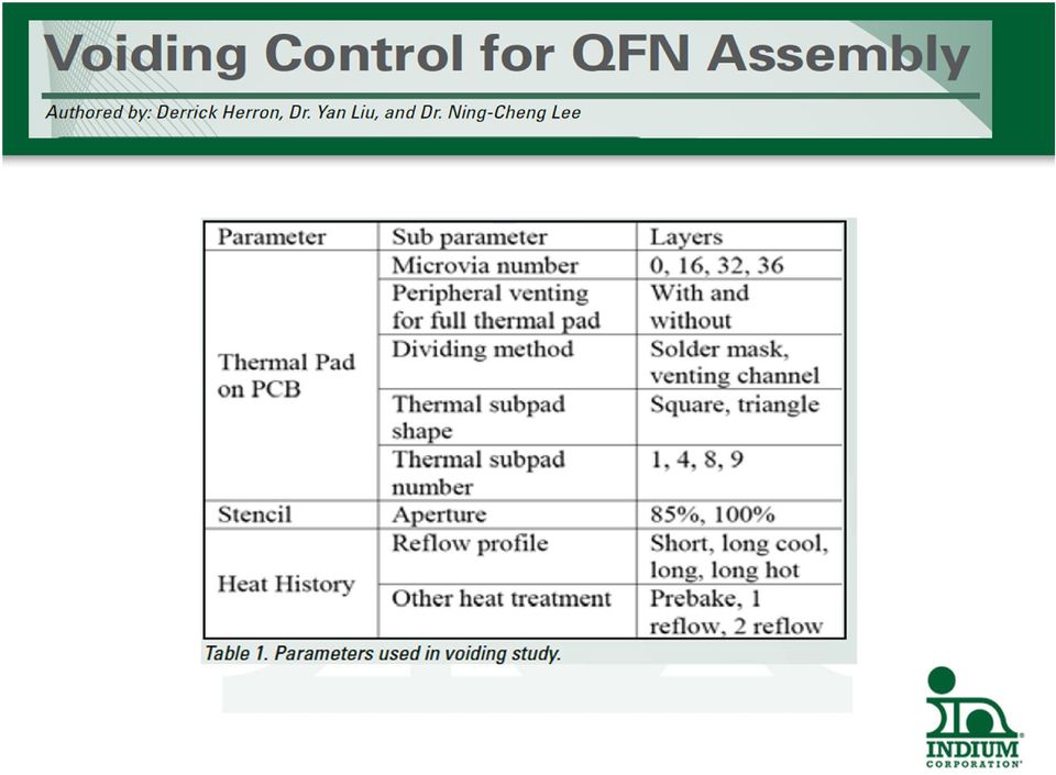
6 Thermal Pad Design Herron, D., Liu, Y., and Lee, N.C.; Voiding Control at QFN Assembly; SMTAi 2011, Fort Worth

7 Notes on Thermal Pad Design Window paning creates pathways to vent volatiles Reduced pockets of volatiles cause smaller voids and less overall voiding Downside: Vent channels result in less solder joint continuity, although selectively Best results for few pathways away from the center Herron, D., Liu, Y., and Lee, N.C.; Voiding Control at QFN Assembly; SMTAi 2011, Fort Worth

8 Results with Optimized Thermal Pads Venting reduces the size of voids, but does not significantly reduce the total voiding area For thermal transfer, large voids are more disruptive -> smaller voids allow for more transfer Solder mask defined pads offer further improvement

9 Thermal Pad Patterning with Solder Mask Results better than with broken up pads, because exposed board between pads can outgas and contribute to voiding Same pattern shows best results Tested via placement under solder mask channels vs. next to channels or scattered Little impact to via placement, vias will often collect a void but there is promise to select via placement to reduce voiding Slide #9

10 Reduce QFN Voiding Through Stencil Design Instead of printing one large square at the center of QFNs: With greater paste volume, voiding increases, so aperture designs that limit paste volume will reduce voiding Break up this square into smaller apertures Spaces between printed areas leave paths for volatiles to escape Larger aperture separations will further reduce voiding For additional information refer to paper: Influence of Reflow Profile and Pb-free Solder Paste in Minimizing Voids for QFN Assembly by T. Jensen, E. Briggs et al.

11 Stencil Design

12 How effective are these process changes? Plating thermal vias with solderable materials minimizes voiding Even with an optimized process and favorable venting, voiding is rarely below 30%, and often 40% In order to reduce voiding to less than 20%, another process improvement is required Placing a solder preform is a viable solution

13 Definition: Solder Preforms Same alloys and metallic properties as solder paste Specified dimensions Offers predictable solder volume optimized for your process

14 Preform dimensions Typically 80% of the QFM ground pad area is appropriate starting point for preform design Preform design: QFN 4 x 4 9 x 9 Thermal Pad 2.15 x x 7.25 Preform 1.83 x x "

15 Flux-coated Preforms Flux coating is necessary to facilitate wetting at the interface with the QFN s pad Composed of predominantly solids, and will not add volatiles under the QFN Promotes wetting, discouraging void propagation Center of QFN Component Flux Coating PCB


16 Preform Thickness vs. Paste Depth Preform thickness should be ~50-70% of paste depth Paste Preform PCB

17 Tape and Reel Design Tape selection: pocket dimensions must be adjusted to minimize travel in the pocket during transport and on the line to minimize mis-picks Special attention to: pitch pocket depth cover tape

18 Pick and Place Parameters Placed preform must be as flat as possible after being placed into the paste Placement force is critical Placement pressure should be increased more than normal levels to insure that the component forms good contact with paste perimeter around the preform Nozzle should be large enough to occupy as much of the surface as possible

19 Reflow Profile Optimization Generally, start out with current profile When using a preform, the best profile is ramp to peak Considering the thermal mass of an assembly, ramp to peak is often not the best option Balance soak to thermal mass, and minimize time to peak Current profile can be optimized toward this goal

20 Process Overview Print paste over entire ground pad Preform sized ~80% of paste area Paste perimeter will provide tack and keep the assembly together before reflow Preform thickness 50-70% of paste depth No-clean flux coating 1.5% by wt. Flux compatibility is required Placement parameters can be optimized for high-volume production Reflow profile allows large window for optimization

21 Parameters for Collaborative Testing QFN thermal pad dimensions (dims): 2mm x 2mm Paste: No-clean solder paste with 89% SAC305, Type 3 PWB pad dims: 2mm x 2mm Stencil dims: 2mm x 2mm x.004 thick Preform alloy: SAC305 Preform dims: 1.7mm x 1.7mm x.002 thick Flux coating: No-clean 1.5% by weight Profile: Adjusted soak The resulting void average was reduced by over 50%.
22 Conclusions Many approaches to reduce QFN voiding, choose those that fit best with process constraints Solutions easily tailored to fit a variety of assemblies Most impactful solution: Add flux-coated preforms to your QFN assembly to: Reduce overall voiding Prevent creating large voids Fortify your process without increasing line time via tape and reel preforms Optimize this strategy to enhance your process
23 Ongoing Work Optimized venting channel size for stencil design and thermal pad design further room for improvement in voiding Additional work optimizing preform process with new flux coating technology Final stages of development for new lowvoiding paste New project: relating voiding performance to thermal performance of components for more application specific optimization Slide #23
24 Questions? Brook Sandy-Smith Product Support Specialist PCB Assembly Materials Indium Corporation JD King Art
Edition 2012-032 Published by Infineon Technologies AG 81726 Munich, Germany 2013 Infineon Technologies AG All Rights Reserved.
 Recommendations for Printed Circuit Board Assembly of Infineon Laminate Packages Additional Information DS1 2012-03 Edition 2012-032 Published by Infineon Technologies AG 81726 Munich, Germany 2013 Infineon
Suggested PCB Land Pattern Designs for Leaded and Leadless Packages, and Surface Mount Guidelines for Leadless Packages
 APPLICATION NOTE Suggested PCB Land Pattern Designs for Leaded and Leadless Packages, and Surface Mount Guidelines for Leadless Packages Introduction This Application Note provides sample PCB land pattern
Choosing a Low-Cost Alternative to SAC Alloys for PCB Assembly
 Choosing a Low-Cost Alternative to SAC Alloys for PCB Assembly Our thanks to Indium Corporation for allowing us to reprint the following article. By Brook Sandy and Ronald C. Lasky, PhD, PE., Indium Corporation
Assembly of LPCC Packages AN-0001
 Assembly of LPCC Packages AN-0001 Surface Mount Assembly and Handling of ANADIGICS LPCC Packages 1.0 Overview ANADIGICS power amplifiers are typically packaged in a Leadless Plastic Chip Carrier (LPCC)
PIN IN PASTE APPLICATION NOTE. www.littelfuse.com
 PIN IN PASTE APPLICATION NOTE 042106 technical expertise and application leadership, we proudly introduce the INTRODUCTION The Pin in Paste method, also called through-hole reflow technology, has become
CASE STUDY: SCREEN PRINTING SOLUTIONS FOR SMALL DIE & PRECISION ALIGNMENT CHALLENGES
 CASE STUDY: SCREEN PRINTING SOLUTIONS FOR SMALL DIE & PRECISION ALIGNMENT CHALLENGES By William E. Coleman Ph.D., Photo Stencil and Travis Tanner, Plexus Manufacturing Solutions When you have a gold Kovar
Molded. By July. A chip scale. and Omega. Guidelines. layer on the silicon chip. of mold. aluminum or. Bottom view. Rev. 1.
 Application Note PAC-006 By J. Lu, Y. Ding, S. Liu, J. Gong, C. Yue July 2012 Molded Chip Scale Package Assembly Guidelines Introduction to Molded Chip Scale Package A chip scale package (CSP) has direct
AND8464/D. Board Level Application Note for 0402, 0502 and 0603 DSN2 Packages APPLICATION NOTE
 Board Level Application Note for 0402, 0502 and 0603 DSN2 Packages Prepared by: Denise Thienpont, Steve St. Germain ON Semiconductor APPLICATION NOTE Introduction ON Semiconductor has introduced an expanded
Investigation for Use of Pin in Paste Reflow Process with Combination of Solder Preforms to Eliminate Wave Soldering
 Investigation for Use of Pin in Paste Reflow Process with Combination of Solder Preforms to Eliminate Wave Soldering Guhan Subbarayan, Scott Priore Assembly Sciences and Technology, Cisco Systems, Inc.
Lead-free Defects in Reflow Soldering
 Lead-free Defects in Reflow Soldering Author: Peter Biocca, Senior Development Engineer, Kester, Des Plaines, Illinois. Telephone 972.390.1197; email pbiocca@kester.com February 15 th, 2005 Lead-free Defects
Customer Service Note Lead Frame Package User Guidelines
 Customer Service Note Lead Frame Package User Guidelines CSN30: Lead Frame Package User Guidelines Introduction Introduction When size constraints allow, the larger-pitched lead-frame-based package design
8-bit Atmel Microcontrollers. Application Note. Atmel AVR211: Wafer Level Chip Scale Packages
 Atmel AVR211: Wafer Level Chip Scale Packages Features Allows integration using the smallest possible form factor Packaged devices are practically the same size as the die Small footprint and package height
Good Boards = Results
 Section 2: Printed Circuit Board Fabrication & Solderability Good Boards = Results Board fabrication is one aspect of the electronics production industry that SMT assembly engineers often know little about.
PCB Land Pattern Design and Surface Mount Guidelines for QFN Packages
 PCB Land Pattern Design and Surface Mount Guidelines for QFN Packages Technical Brief 389 Authors: Mark Kwoka and Jim Benson Introduction Intersil's Quad Flat No Lead (QFN) package family offering is a
Edition 2012-05 Published by Infineon Technologies AG 81726 Munich, Germany 2012 Infineon Technologies AG All Rights Reserved.
 Recommendations for Printed Circuit Board Assembly of Infineon QFN Packages Additional Information DS7, 2012-05 Edition 2012-05 Published by Infineon Technologies AG 81726 Munich, Germany 2012 Infineon
noclean Characterization of No-Clean Solder Paste Residues: The Relationship to In-Circuit Testing
 Characterization of No-Clean Solder Paste Residues: The Relationship to In-Circuit Testing Many manufacturers have now completed the conversion to no clean solder paste. Many factors governed this initial
How to avoid Layout and Assembly got chas with advanced packages
 How to avoid Layout and Assembly got chas with advanced packages Parts and pitch get smaller. Pin counts get larger. Design cycles get shorter. BGA, MicroBGA, QFN, DQFN, CSP packages are taking the design
SURFACE FINISHING FOR PRINTED CIRCUIT BOARDS
 SURFACE FINISHING FOR PRINTED CIRCUIT BOARDS In a world of ever-increasing electronic component complexity and pin count requirements for component packaging, focus is once again on the age-old question
Handling, soldering & mounting instructions
 Tri-axial acceleration sensor SMB380 SMB380 Order code 0 273 141 006 Package type QFN Release version 1.0 Release date 2007-07-23 Notes Rev. 1.0 Specifications are Page subject 1 to change without notice
ALPHA OL-107F-A ZERO-HALOGEN, LOW VOIDS, FINE FEATURE, EXCELLENT PIN TEST PERFORMANCE, NO-CLEAN, LEAD-FREE SOLDER PASTE
 T E C H N I C A L B U L L E T I N ALPHA OL-107F-A ZERO-HALOGEN, LOW VOIDS, FINE FEATURE, EXCELLENT PIN TEST PERFORMANCE, NO-CLEAN, LEAD-FREE SOLDER PASTE DESCRIPTION ALPHA OL-107F-A is a lead-free, Zero-halogen
Solder Reflow Guide for Surface Mount Devices
 June 2015 Introduction Technical Note TN1076 This technical note provides general guidelines for a solder reflow and rework process for Lattice surface mount products. The data used in this document is
JOHANSON DIELECTRICS INC. 15191 Bledsoe Street, Sylmar, Ca. 91342 Phone (818) 364-9800 Fax (818) 364-6100
 364-9800 Fax (818) 364-6100") Arc Season and Board Design Observations John Maxwell, Director of Product Development, Johanson Dielectrics Inc. Enrique Lemus, Quality Engineer, Johanson Dielectrics Inc. This years arcing season is
Arc Season and Board Design Observations John Maxwell, Director of Product Development, Johanson Dielectrics Inc. Enrique Lemus, Quality Engineer, Johanson Dielectrics Inc. This years arcing season is
Flux gel is available in 10 and 30 cc syringes for rework applications Complies with RoHS Directive 2002/95/EC
 DESCRIPTION ALPHA CVP-390 is a lead-free, Zero-halogen no-clean solder paste designed for applications where residue with excellent pin testing property and ability to pass JIS Copper Corrosion test are
ALPHA CVP-390 - NO-CLEAN, LEAD-FREE SOLDER PASTE ZERO-HALOGEN, LOW VOIDS, FINE FEATURE, EXCELLENT PIN TEST PERFORMANCE, SAC305 AND LOW AG CAPABLE.
 T E C H N I C A L B U L L E T I N ALPHA CVP-390 - NO-CLEAN, LEAD-FREE SOLDER PASTE ZERO-HALOGEN, LOW VOIDS, FINE FEATURE, EXCELLENT PIN TEST PERFORMANCE, SAC305 AND LOW AG CAPABLE. DESCRIPTION ALPHA CVP-390
RoHS-Compliant Through-Hole VI Chip Soldering Recommendations
 APPLICATION NOTE AN:017 RoHS-Compliant Through-Hole VI Chip Soldering Recommendations Ankur Patel Associate Product Line Engineer Contents Page Introduction 1 Wave Soldering 1 Hand Soldering 4 Pin/Lead
Application Note AN-0994 Maximizing the Effectiveness of your SMD Assemblies
 Application Note AN-0994 Maximizing the Effectiveness of your SMD Assemblies Table of Contents Page Method...2 Thermal characteristics of SMDs...2 Adhesives...4 Solder pastes...4 Reflow profiles...4 Rework...6
Cree XLamp XP-G LEDs Data Sheet
 Cree XLamp XP-G LEDs Data Sheet The XLamp XP-G LED delivers unprecedented levels of light output and efficacy for a single die LED. The XLamp XP-G LED continues Cree s history of innovation in LEDs for
Flip Chip Package Qualification of RF-IC Packages
 Flip Chip Package Qualification of RF-IC Packages Mumtaz Y. Bora Peregrine Semiconductor San Diego, Ca. 92121 mbora@psemi.com Abstract Quad Flat Pack No Leads (QFNs) are thermally enhanced plastic packages
Antenna Part Number: FR05-S1-R-0-105
 Fractus EZConnect Zigbee, RFID, ISM868/9 Chip Antenna Antenna Part Number: FR5-S1-R--15 This product is protected by at least the following patents PAT. US 7,148,85, US 7,22,822 and other domestic and
Features. Typical Applications G9. ProLight PEA2-3FVE 3W Warm White AC LED Technical Datasheet Version: 1.7 1 DS-0042
 ProLight PEA2-3FVE 3W Warm White AC LED Technical Datasheet Version: 1.7 Features High Color rendering index Follow ANSI C78.788.2008 Chromaticity co-ordinates High flux per LED Good color uniformity Industry
Analysis of BGA Solder Joint Reliability for Selected Solder Alloy and Surface Finish Configurations
 Analysis of BGA Solder Joint Reliability for Selected Solder Alloy and Surface Finish Configurations Hugh Roberts / Atotech USA Inc Sven Lamprecht and Christian Sebald / Atotech Deutschland GmbH Mark Bachman,
B Recommended land pattern: [mm] C Stencil suggestion: 2015-03-11. SSt. SKl CHECKED DATE
![B Recommended land pattern: [mm] C Stencil suggestion: 2015-03-11. SSt. SKl CHECKED DATE](/thumbs/40/21834432.jpg "B Recommended land pattern: [mm] C Stencil suggestion: 2015-03-11. SSt. SKl CHECKED DATE") A Dimensions: [mm] B Recommended land pattern: [mm] D Properties: Properties Surface Material Thread Tightening torque Solder Cream Thickness Packaging Value Tin plated 11SMnPb30 M2.5 0.35 Nm 150 µm Reel
A Dimensions: [mm] B Recommended land pattern: [mm] D Properties: Properties Surface Material Thread Tightening torque Solder Cream Thickness Packaging Value Tin plated 11SMnPb30 M2.5 0.35 Nm 150 µm Reel
Auditing Contract Manufacturing Processes
 Auditing Contract Manufacturing Processes Greg Caswell and Cheryl Tulkoff Introduction DfR has investigated multiple situations where an OEM is experiencing quality issues. In some cases, the problem occurs
Technical Note Recommended Soldering Parameters
 Technical Note Recommended Soldering Parameters Introduction Introduction The semiconductor industry is moving toward the elimination of Pb from packages in accordance with new international regulations.
PCB Assembly Guidelines for Intersil Wafer Level Chip Scale Package Devices
 Assembly Guidelines for Intersil Wafer Level Chip Scale Package Devices Introduction There is an industry-wide trend towards using the smallest package possible for a given pin count. This is driven primarily
WE-CBF SMD EMI Suppression Ferrite Bead
 A Dimensions: [mm] B Recommended land pattern: [mm] D Electrical Properties: Properties Test conditions Value Unit Tol. Impedance @ 100 MHz 100 MHz Z 600 Ω ±25% Maximum impedance 80 MHz Z 650 Ω typ. Rated
uclamp0541z Ultra Small μclamp 1-Line ESD Protection
 - Z-Pak TM Description μclamp TVS diodes are designed to protect sensitive electronics from damage or latch-up due to ESD. It is designed to replace 2 size multilayer varistors (MLVs) in portable applications
Quad Flat Package (QFP)
") Freescale Semiconductor Application Note AN4388 Rev. 2.0, 2/2014 Quad Flat Package (QFP) 1 Introduction This document provides guidelines for handling and assembly of Freescale QFP packages during Printed
Freescale Semiconductor Application Note AN4388 Rev. 2.0, 2/2014 Quad Flat Package (QFP) 1 Introduction This document provides guidelines for handling and assembly of Freescale QFP packages during Printed
Bob Willis leadfreesoldering.com
 Assembly of Flexible Circuits with Lead-Free Solder Alloy Bob Willis leadfreesoldering.com Introduction to Lead-Free Assembly Video Clips Component www.bobwillis.co.uk/lead/videos/components.rm Printed
Surface mount reflow soldering
 Surface mount reflow soldering Rev. 6 30 July 2012 Application note Document information Info Keywords Abstract Content surface mount, reflow soldering, component handling This application note provides
SMD Power Elements Design Guide. 50 A SMD Technology Small Size High Current
 SMD Power Elements Design Guide 50 A SMD Technology Small Size High Current Contents Surface Mount Technology & Assembly Surface Pad Geometry & Stencil Technical Data Qualification Reliability Test 2 www.we-online.com
3D Electroform Stencils for Two Level PCB
 3D Electroform Stencils for Two Level PCB Rachel Miller-Short, VP Global Sales Photo Stencil Bill Coleman Photo Stencil Dudi Amir Intel Joe Perault Parmi Abstract The requirements for two-level PCB with
Handling and Processing Details for Ceramic LEDs Application Note
 Handling and Processing Details for Ceramic LEDs Application Note Abstract This application note provides information about the recommended handling and processing of ceramic LEDs from OSRAM Opto Semiconductors.
Fractus Compact Reach Xtend
 Fractus Compact Reach Xtend Bluetooth, Zigbee, 82.11 b/g/n WLAN Chip Antenna Antenna Part Number: FR5-S1-N--12 This product is protected by at least the following patents PAT. US 7,148,85, US 7,22,822
GUIDELINES FOR PRINTED CIRCUIT BOARD ASSEMBLY (PCBA) OF UTAC GROUP S GRID ARRAY PACKAGE (GQFN) AND ITS BOARD LEVEL RELIABILITY
 OF UTAC GROUP S GRID ARRAY PACKAGE (GQFN) AND ITS BOARD LEVEL RELIABILITY") GUIDELINES FOR PRINTED CIRCUIT BOARD ASSEMBLY (PCBA) OF UTAC GROUP S GRID ARRAY PACKAGE (GQFN) AND ITS BOARD LEVEL RELIABILITY Kyaw Ko Lwin*, Daniel Ting Lee Teh, Carolyn Epino Tubillo, Jun Dimaano, Ang
GUIDELINES FOR PRINTED CIRCUIT BOARD ASSEMBLY (PCBA) OF UTAC GROUP S GRID ARRAY PACKAGE (GQFN) AND ITS BOARD LEVEL RELIABILITY Kyaw Ko Lwin*, Daniel Ting Lee Teh, Carolyn Epino Tubillo, Jun Dimaano, Ang
DVD-111C Advanced Hand Soldering Techniques
 DVD-111C Advanced Hand Soldering Techniques Below is a copy of the narration for DVD-111C. The contents for this script were developed by a review group of industry experts and were based on the best available
Be the best. PCBA Design Guidelines and DFM Requirements. Glenn Miner Engineering Manager March 6, 2014 DFM DFT. DFx DFC DFQ
 and DFM Requirements DFM DFQ DFx DFT DFC Glenn Miner Engineering Manager Electronics, Inc. Not to be reproduced or used in any means without written permission by Benchmark. Guidelines and Requirements
Product family data sheet
 Cree XLamp MX-6 LEDs Product family data sheet CLD-DS23 Rev 3A Product Description The Cree XLamp MX-6 LED provides the proven lightingclass performance and reliability of Cree XLamp LEDs in a flat-top
Mounting of Meritec SMT Products Using Lead-Free Solder
 Mounting of Meritec SMT Products Using Lead-Free Solder 10/10/08 rev B Mounting of Meritec SMT Products Using Lead-Free Solder Contents Page 2 Scope Page 3 Test Samples/Preparation Page 3 Facilities/Equipment
Available in white (2,600 K to 8,300 K CCT) Maximum drive current: 1000 ma. Wide viewing angle: 120. Electrically neutral thermal path
 Maximum drive current: 1000 ma. Wide viewing angle: 120. Electrically neutral thermal path") PRODUCT FAMILY DATA SHEET CLD-23 REV 3 Cree XLamp MX-6 LEDs PRODUCT DESCRIPTION The Cree XLamp MX-6 LED provides the proven lighting-class performance and reliability of Cree XLamp LEDs in a flat-top PLCC
PRODUCT FAMILY DATA SHEET CLD-23 REV 3 Cree XLamp MX-6 LEDs PRODUCT DESCRIPTION The Cree XLamp MX-6 LED provides the proven lighting-class performance and reliability of Cree XLamp LEDs in a flat-top PLCC
SLG7NT4129 PCIE RTD3. Pin Configuration. Features Low Power Consumption Dynamic Supply Voltage RoHS Compliant / Halogen-Free Pb-Free TDFN-12 Package
 General Description Silego SLG7NT4129 is a low power and small form device. The SoC is housed in a 2.5mm x 2.5mm TDFN package which is optimal for using with small devices. Features Low Power Consumption
CLA4607-085LF: Surface Mount Limiter Diode
 DATA SHEET CLA4607-085LF: Surface Mount Limiter Diode Applications Low-loss, high-power limiters Receiver protectors Anode (Pin 1) Anode (Pin 3) Features Low thermal resistance: 55 C/W Typical threshold
Lead-Free Rework Optimization Project
 Lead-Free Rework Optimization Project Project Co-Chairs: Jasbir Bath, Flextronics International Craig Hamilton, Celestica IPC APEX 2008 Background Reliability tests in the previous inemi lead-free assembly
17 IMPLEMENTATION OF LEAD-FREE SOLDERING TECHNOLOGY. Eva Kotrčová České Vysoké Učení Technické Fakulta Elektrotechnická Katedra Elektrotechnologie
 17 IMPLEMENTATION OF LEAD-FREE SOLDERING TECHNOLOGY Eva Kotrčová České Vysoké Učení Technické Fakulta Elektrotechnická Katedra Elektrotechnologie 1. Introduction Lead is the toxic heavy metal which is
SMT Troubleshooting Guide
 SMT Troubleshooting Guide Easy-to-use advice for common SMT assembly issues. Cookson Electronics Troubleshooting Guide Table of Contents With this easy-to-use Troubleshooting Guide, you can learn to troubleshoot
Cree XLamp MX-6 LEDs Data Sheet
 Cree XLamp MX-6 LEDs Data Sheet The Cree XLamp MX-6 LED provides the proven lighting-class performance and reliability of Cree XLamp LEDs in a flat-top PLCC package. The XLamp MX-6 LED continues Cree s
APPLICATION NOTE PCB Design and SMT Assembly/Rework Guidelines for MCM-L Packages
 APPLICATION NOTE PCB Design and SMT Assembly/Rework Guidelines for MCM-L Packages REVISION HISTORY Revision Level Date Description A August 2001 Initial Release B January 17, 2002 C July 18, 2002 D July
TN0991 Technical note
 Technical note Description of WLCSP for STMicroelectronics EEPROMs and recommendations for use Introduction This document describes the 5 and 8-bump WLCSPs (wafer level chip size package) used for STMicroelectronics
Processing of SMD LEDs Application note
 Processing of SMD LEDs Application note Abstract This application note provides a basic overview of the essential aspects and influencing factors regarding the processing of SMD LEDs. Introduction In general,
Mounting Instructions for SP4 Power Modules
 Mounting Instructions for SP4 Power Modules Pierre-Laurent Doumergue R&D Engineer Microsemi Power Module Products 26 rue de Campilleau 33 520 Bruges, France Introduction: This application note gives the
Product Specification
 Product Specification Model No.: DC-240-L01-00-TR Description: H=3.00mm Horizontal SMD DC Power Jacks Pin Shaft Diameter: 0.65mm Packing Method: Tape & Reel (600pcs./R) 1. General 1a. Scope The jacks should
Figure 1 (end) Application Specification 114 13088 provides application requirements for MICTOR Right Angle Connectors for SMT PC Board Applications
 Application Specification 114 13088 provides application requirements for MICTOR Right Angle Connectors for SMT PC Board Applications") This specification covers requirements for application of MICTOR Vertical Board to Board Plugs and Receptacles designed for pc boards. The connectors have an in row contact spacing on 0.64 [.025] centerlines.
This specification covers requirements for application of MICTOR Vertical Board to Board Plugs and Receptacles designed for pc boards. The connectors have an in row contact spacing on 0.64 [.025] centerlines.
Q&A. Contract Manufacturing Q&A. Q&A for those involved in Contract Manufacturing using Nelco Electronic Materials
 Q&A Q&A for those involved in Contract Manufacturing using Nelco Electronic Materials 1. Do Nelco laminates have any discoloration effects or staining issues after multiple high temperature exposures?
Selective Soldering Defects and How to Prevent Them
 Selective Soldering Defects and How to Prevent Them Gerjan Diepstraten Vitronics Soltec BV Introduction Two major issues affecting the soldering process today are the conversion to lead-free soldering
SM712 Series 600W Asymmetrical TVS Diode Array
 SM712 Series 6W Asymmetrical TVS Diode Array RoHS Pb GREEN Description The SM712 TVS Diode Array is designed to protect RS-485 applications with asymmetrical working voltages (-7V to from damage due to
N35L-U High Power LED
 N35L-U High Power LED Introduction The N35L-U LED from SemiLEDs brings industry leading technology to the solid state lighting market with its high quality and performance. With a silicone lens, N35L-U
Application Note AN-1170. Audio Power Quad Flat No-Lead (PQFN) Board Mounting Application Note
 Board Mounting Application Note") Application Note AN-1170 Audio Power Quad Flat No-Lead (PQFN) Board Mounting Application Note Table of Contents Page Device construction...2 Design considerations...3 Assembly considerations...4 Mechanical
Application Note AN-1170 Audio Power Quad Flat No-Lead (PQFN) Board Mounting Application Note Table of Contents Page Device construction...2 Design considerations...3 Assembly considerations...4 Mechanical
Introduction to the Plastic Ball Grid Array (PBGA)
") Introduction to the Plastic Ball Grid Array (PBGA) Q1, 2008 Terry Burnette Dec. 15, 2005 Presentation Outline PBGA Introduction and Package Description PC Board Design for PBGA PBGA Assembly PBGA Solder
Introduction to the Plastic Ball Grid Array (PBGA) Q1, 2008 Terry Burnette Dec. 15, 2005 Presentation Outline PBGA Introduction and Package Description PC Board Design for PBGA PBGA Assembly PBGA Solder
A and M Electronics Contract Manufacturing Circuit Board Assembly 25018 Avenue Kearny Valencia, Ca. 91355 (661) 257-3680 or (800) 923-3058
 257-3680 or (800) 923-3058") A and M Electronics Contract Manufacturing Circuit Board Assembly 25018 Avenue Kearny Valencia, Ca. 91355 (661) 257-3680 or (800) 923-3058 "When Quality Counts, Choose A&M Electronics" SMT, BGA, & Through
A and M Electronics Contract Manufacturing Circuit Board Assembly 25018 Avenue Kearny Valencia, Ca. 91355 (661) 257-3680 or (800) 923-3058 "When Quality Counts, Choose A&M Electronics" SMT, BGA, & Through
PCB Board Design. PCB boards. What is a PCB board
 PCB Board Design Babak Kia Adjunct Professor Boston University College of Engineering Email: bkia -at- bu.edu ENG SC757 - Advanced Microprocessor Design PCB boards What is a PCB board Printed Circuit Boards
Electronic Board Assembly
 Electronic Board Assembly ERNI Systems Technology Systems Solutions - a one stop shop - www.erni.com Contents ERNI Systems Technology Soldering Technologies SMT soldering THR soldering THT soldering -
Hand Soldering Basics
 Technical Note Hand Soldering Basics Table of Contents Abstract...1 Process Control...1 Tip Selection...2 Temperature Selection...3 Flux Selection...4 Soldering Techniques...5 Soldering Iron Tip Plating
Cree XLamp XP-G LEDs PRODUCT FAMILY DATA SHEET PRODUCT DESCRIPTION FEATURES TABLE OF CONTENTS CLD-DS20 REV 4
 PRODUCT FAMILY DATA SHEET CLD-DS20 REV 4 Cree XLamp XP-G LEDs PRODUCT DESCRIPTION The XLamp XP-G LED delivers unprecedented levels of light output and efficacy for a single die LED. The XLamp XP-G LED
Analog Devices Welcomes Hittite Microwave Corporation NO CONTENT ON THE ATTACHED DOCUMENT HAS CHANGED
 Analog Devices Welcomes Hittite Microwave Corporation NO CONTENT ON THE ATTACHED DOCUMENT HAS CHANGED www.analog.com www.hittite.com THIS PAGE INTENTIONALLY LEFT BLANK Typical Applications The HMC547LP3
HLMP-1600, HLMP-1601, HLMP-1620, HLMP-1621 HLMP-1640, HLMP-1641, HLMP-3600, HLMP-3601 HLMP-3650, HLMP-3651, HLMP-3680, HLMP-3681
 HLMP-16, HLMP-161, HLMP-162, HLMP-1621 HLMP-16, HLMP-161, HLMP-36, HLMP-361 HLMP-365, HLMP-3651, HLMP-368, HLMP-3681 T 1 3 / (5 mm), T-1 (3 mm), 5 Volt, 12 Volt, Integrated Resistor LED Lamps Data Sheet
Recommendations for Printed Circuit Board Assembly of Infineon WLL Packages
 Recommendations for Printed Circuit Board Assembly of Infineon WLL Application Note Please read the Important Notice and Warnings at the end of this document www.infineon.com Table of Contents Table
Cree XLamp XR-E LED. Table of Contents. CLD-DS05 Rev 16B. Product family data sheet
 Cree XLamp XR-E LED Product family data sheet CLD-DS05 Rev 16B Product Description The XLamp XR-E LED is leading the LED lighting revolution with its unprecedented lighting-class brightness, efficacy,
RIGHT ANGLE CLINCH FASTENERS BULLETIN
 BULLETIN R 215 R e v 515 PEM R NGLE fasteners provide strong right angle attachment points in sheet metal or PC boards. Types R and RS for metal are simply pressed into a rectangular mounting hole of the
MADP-000504-10720T. Non Magnetic MELF PIN Diode
 MADP-54-172T Features High Power Handling Low Loss / Low Distortion Leadless Low Inductance MELF Package Non-Magnetic Surface Mountable RoHS Compliant MSL 1 Package Style 172 Dot Denotes Cathode Description
PCB inspection is more important today than ever before!
 PCB inspection is more important today than ever before! Industry experts continue to stress the need to inspect hidden solder joints! Figure 1. The BGA package has not been placed into the paste deposit.
B Recommended land pattern: [mm] SSt. SSt 2014-07-15 2014-05-12. SSt. SSt. SSt 2014-01-07. SSt 2013-11-19. SSt. SBa. SSt 2013-04-24.
![B Recommended land pattern: [mm] SSt. SSt 2014-07-15 2014-05-12. SSt. SSt. SSt 2014-01-07. SSt 2013-11-19. SSt. SBa. SSt 2013-04-24.](/thumbs/17/124841.jpg "B Recommended land pattern: [mm] SSt. SSt 2014-07-15 2014-05-12. SSt. SSt. SSt 2014-01-07. SSt 2013-11-19. SSt. SBa. SSt 2013-04-24.") A Dimensions: [mm] B Recommended land pattern: [mm] D Electrical Properties: Properties Test conditions Value Unit Tol. Inductance 1 khz/ 100 mv L 2x 51 µh ±30% Impedance Z max 5500 Ω typ. Rated current
A Dimensions: [mm] B Recommended land pattern: [mm] D Electrical Properties: Properties Test conditions Value Unit Tol. Inductance 1 khz/ 100 mv L 2x 51 µh ±30% Impedance Z max 5500 Ω typ. Rated current
Metal-Oxide Varistors (MOVs) Surface Mount Multilayer Varistors (MLVs) > MLN Series. MLN SurgeArray TM Suppressor. Description
 Surface Mount Multilayer Varistors (MLVs) > MLN Series. MLN SurgeArray TM Suppressor. Description") MLN SurgeArray TM Suppressor RoHS Description The MLN SurgeArray Suppressor is designed to help protect components from transient voltages that exist at the circuit board level. This device provides four
MLN SurgeArray TM Suppressor RoHS Description The MLN SurgeArray Suppressor is designed to help protect components from transient voltages that exist at the circuit board level. This device provides four
Copyright 2008 IEEE. Reprinted from ECTC2008 Proceedings.
 Copyright 2008 IEEE. Reprinted from ECTC2008 Proceedings. This material is posted here with permission of the IEEE. Such permission of the IEEE does not in any way imply IEEE endorsement of any of Amkor
Discontinued. LUXEON V Portable. power light source. Introduction
 Preliminary Technical Datasheet DS40 power light source LUXEON V Portable Introduction LUXEON is a revolutionary, energy efficient and ultra compact new light source, combining the lifetime and reliability
WL-SWTC SMD White Top View Ceramic LED
 A Dimensions: [mm] B Recommended land pattern: [mm] D Absolute Maximum Ratings (Ambient Temperature 25 C): Properties Test conditions Value Unit Power dissipation P Diss 2.52 W Peak Forward Current duty/10@1khz
T5050M-MCL1 High Power Mixing Color LED
 PRODUCT DATASHEET T5050M-MCL1 High Power Mixing Color LED Introduction The T5050M-MCL1 LED from TSLC brings industry leading technology to the solid state lighting market with its high quality and performance.
Application Note AN-1136. Discrete Power Quad Flat No-Lead (PQFN) Board Mounting Application Note
 Board Mounting Application Note") Application Note AN-1136 Discrete Power Quad Flat No-Lead (PQFN) Board Mounting Application Note Table of Contents Page Introduction...2 Device construction...2 Design considerations...3 Assembly considerations...4
Application Note AN-1136 Discrete Power Quad Flat No-Lead (PQFN) Board Mounting Application Note Table of Contents Page Introduction...2 Device construction...2 Design considerations...3 Assembly considerations...4
Recommended Soldering Techniques for ATC 500 Series Capacitors
 Recommended Soldering Techniques for ATC 500 Series Capacitors ATC# 001-884 Rev. D; 10/05 1.0. SCOPE. The following procedures have been successful in soldering ATC500 series capacitors to both soft and
AN-617 Application Note
 One Technology Way P.O. Box 9106 Norwood, MA 02062-9106, U.S.A. Tel: 781.329.4700 Fax: 781.461.3113 www.analog.com Wafer Level Chip Scale Package by the Wafer Level Package Development Team GENERAL DESCRIPTION
Cree XLamp MX-3S LEDs Data Sheet
 Cree XLamp MX-3S LEDs Data Sheet The Cree XLamp MX-3S LED provides the proven lighting-class performance and reliability of Cree XLamp LEDs in a high voltage, PLCC configuration. All members of the MX-family
HOT BAR REFLOW SOLDERING FUNDAMENTALS. A high quality Selective Soldering Technology
 HOT BAR REFLOW SOLDERING FUNDAMENTALS A high quality Selective Soldering Technology Content 1. Hot Bar Reflow Soldering Introduction 2. Application Range 3. Process Descriptions > Flex to PCB > Wire to
For board-to-fpc. Narrow Pitch Connectors (0.35mm pitch)
") For board-to-fpc Narrow Pitch Connectors (0.35mm pitch) S35 Series New FEATURES 1. 1.7 mm wide slim two-piece type connector Mated height 0.6 mm Smaller compared to A4F series Width: Approx. 44% down
For board-to-fpc Narrow Pitch Connectors (0.35mm pitch) S35 Series New FEATURES 1. 1.7 mm wide slim two-piece type connector Mated height 0.6 mm Smaller compared to A4F series Width: Approx. 44% down
LUXEON C Series. Proper handling, assembly, board design and thermal management are required for high optical output and reliability.
 LUXEON C Series Assembly and Handling Information Application Brief AB36 LUXEON C Series Assembly and Handling Information Introduction LUXEON C series is the power LED that enables manufacturers of appliances,
Designing with High-Density BGA Packages for Altera Devices
 2014.12.15 Designing with High-Density BGA Packages for Altera Devices AN-114 Subscribe As programmable logic devices (PLDs) increase in density and I/O pins, the demand for small packages and diverse
SM Series 400W TVS Diode Array
 General Purpose ESD Protection - SM5 through SM3 SM Series W TVS Diode Array RoHS Pb GREEN Description The SM series TVS Diode Array is designed to protect sensitive equipment from damage due to electrostatic
0.3 mm Contact Pitch, 0.9 mm above the board, Flexible Printed Circuit ZIF Connectors.
 0.3 mm Contact Pitch, 0.9 mm above the board, Flexible Printed Circuit ZIF Connectors. FH Series (51pos. type) 3.45mm 17.1mm 0.9mm Features 1. Extremely light weight The largest version, with all contacts
Flex Circuit Design and Manufacture.
 Flex Circuit Design and Manufacture. Hawarden Industrial Park, Manor Lane, Deeside, Flintshire, CH5 3QZ Tel 01244 520510 Fax 01244 520721 Sales@merlincircuit.co.uk www.merlincircuit.co.uk Flex Circuit
NARROW-PITCH (0.8mm) CONNECTORS P8 SERIES
 CONNECTORS P8 SERIES") Socket Header Compliance with RoHS Directive NRROW-PITCH CONNECTORS FOR PC ORDS 3. Perfect for portable devices, the bellows-type provide a strong resistance against falling, impacts, and forced insertions
Socket Header Compliance with RoHS Directive NRROW-PITCH CONNECTORS FOR PC ORDS 3. Perfect for portable devices, the bellows-type provide a strong resistance against falling, impacts, and forced insertions
Evaluation of Soft Soldering on Aluminium Nitride (AlN) ESTEC Contract No. 19220/05/NL/PA. CTB Hybrids WG ESTEC-22nd May 2007
 ESTEC Contract No. 19220/05/NL/PA. CTB Hybrids WG ESTEC-22nd May 2007") Evaluation of Soft Soldering on Aluminium Nitride (AlN) ESTEC Contract No. 19220/05/NL/PA CTB Hybrids WG ESTEC-22nd May 2007 Evaluation of Soft Soldering on AlN Schedule Project presentation Feasibility
Evaluation of Soft Soldering on Aluminium Nitride (AlN) ESTEC Contract No. 19220/05/NL/PA CTB Hybrids WG ESTEC-22nd May 2007 Evaluation of Soft Soldering on AlN Schedule Project presentation Feasibility
How To Clean A Copper Board With A Socket On It (Ios)
") Den-on Rework Reference Process for Desktop platform and new Intel Socket LGA-1156 using the Den-on BGA rework station RD-500II and III *This document shows the whole process on how to repair the Intel
Den-on Rework Reference Process for Desktop platform and new Intel Socket LGA-1156 using the Den-on BGA rework station RD-500II and III *This document shows the whole process on how to repair the Intel