How To Increase Memory Bandwidth On A Memory Card With A Memory Module (Dird)
|
|
|
- Leona Newman
- 3 years ago
- Views:
Transcription
1 Memory - DDR1, DDR2, and DDR3 Brought to you by please visit our site! DDR1 Double Data Rate-SDRAM, or simply DDR1, was designed to replace SDRAM. DDR1 was originally referred to as DDR-SDRAM or simple DDR. When DDR2 was introduced, DDR became referred to as DDR1. Names of components constantly change as newer technologies are introduced, especially when the newer technology is based on a previous e one. The principle applied in DDR is exactly as the name implies double data rate. The DDR actually doubles the rate data is transferred by using both the rising and falling edges of a typical digital pulse. Earlier memory technology such as SDRAM transferred data after one complete digital pulse. DDR transfers data twice as fast by transferring data on both the rising and falling edges of the digital pulse. Look at figure below. DDR Digital Pulse As you can see in the drawing, DDR can transfer twice the amount of data per single digital pulse by using both the rising edge, and the falling edge of the digital signal. DDR can transfer twice the data as SDRAM.

2 DDR2 DDR2 is the next generation of memory developed after DDR. DDR2 increased the data transfer rate referred to as bandwidth by increasing the operational frequency to match the high FSB frequencies and by doubling the prefetch buffer data rate. There will be more about the memory prefetch buffer data rate later in this section. DDR2 is a 240 pin DIMM design that operates at 1.8 volts. The lower voltage counters the heat effect of the higher frequency data transfer. DRR operates at 2.5 volts and is a 188 pin DIMM design. DDR2 uses a different motherboard socket than DDR, and is not compatible with motherboards designed for DDR. The DDR2 DIMM key will not align with DDR DIMM key. If the DDR2 is forced into the DDR socket, it will damage the socket and the memory will be exposed to a high voltage level. Also be aware the DDR is 188 pin DIMM design and DDR2 is a 240 pin DIMM design. DDR3 DDR3 was the next generation memory introduced in the summer of 2007 as the natural successor to DDR2. DDR3 increased the pre-fetch buffer size to 8-bits an increased the operating frequency once again resulting in high data transfer rates than its predecessor DDR2. In addition, to the increased data transfer rate memory chip voltage level was lowered to 1.5 V to counter the heating effects of the high frequency. By now you can see the trend of memory to increase pre-fetch buffer size and chip operating frequency, and lowering the operational voltage level to counter heat. The physical DDR3 is also designed with 240 pins, but the notched key is in a different position to prevent the insertion into a motherboard RAM socket designed for DDR2. DDR3 is both electrical and physically incompatible with previous versions of RAM. In addition to high frequency and lower applied voltage level, the DDR3 has a memory reset option which DDR2 and DDR1 do not. The memory reset allows the memory to be cleared by a software reset action. Other memory types do not have this feature which means the memory state is uncertain after a system reboot. The memory reset feature insures that the memory will be clean or empty after a system reboot. This feature will result in a more stable memory system. DDR3 uses the same 240-pin design as DDR2, but the memory module key notch is at a different location.

3 Compare DDR Prefetch, Chip Voltage and Data Rates for Motherboard FSB. DDR1 DDR2 DDR3 Prefetch Buffer 2-bits 4-bits 8-bits Voltage level 2.5 V 1.8 V 1.5 V FSB Data Rates expressed as MHz 200,266,333, , 533, 677, ,1066,1330,1600 Memory Module PC Classification Memory Chip Classification Memory Module Bandwidth PC100 SDRAM 800 MB PC133 SDRAM 1.1 GB PC1600 DDR 1.6 GB PC2100 DDR 2.1GB PC2700 DDR 2.7GB PC DDR GB PC DDR GB PC DDR GB PC DDR GB PC DDR GB PC DDR GB PC DDR GB PC DDR GB PC DDR GB Note: The chart is based on theoretical throughputs, and do not take in account the memory controller, BIOS, or chip set. For a motherboard designed with dual channel architecture, the memory module bandwidth is effectively doubled theoretically. The memory Chip Classification correlates to the memory chip frequency design. For example, a DDR2-400 is designed to operate at 400 MHz. The memory module PC classification correlates to the memory module frequency times 8. For example A DDR2-400 would be identified as a PC The 3200 is equal to 8 times the 400 MHz.

4 The memory module band width is the theoretical amount of data that can be transferred expressed in the chart as Giga Bytes. This is the measurement of expected system performance. Also be aware that the expected performance can double when the motherboard memory transfer design is dual channel. Note: You will see many video cards with a specification of GDDR3 as the main memory type mounted on the video card. Do not confuse this with DDR3; GDDR3 is only designed for video cards. DDR Pre-fetch Memory Buffer Memory chips can operate at extremely high frequencies inside the memory chip structure. The frequencies of the individual electronic logic transistors inside the chip operate at a much higher frequency than the outside connections such as the FBS or the HyperTransport bus. The transferring data is positioned into a buffer located on the chip and then awaits the proper time to transfer the data to the bus on the motherboard. The entire operating is referred to as the memory prefetch. The term pre-fetch is followed by the lower case letter n and a number, which represents the number of data bits. For example, DDR1 has a pre-fetch 2n, which means it can store 2-bits of data in each pre-fetch buffer. DDR2 uses a prefetch 4n, or 4-bit buffer thus doubling the amount of data transfer from the buffer as compared to DDR1. DDR3 uses a prefect 8n which double the size of prefetch used in DDR2. The increased size of the pre-fetch buffer, and the increased memory bus operational frequency lets each generation of DDR increase the overall throughput. The overall throughput of the various DDR RAM speeds is only a theoretical throughput, even though it is expressed as exact values such as 12.8 GB. The 12.8 GB is the theoretical data transfer rate, and does not account for other devices using the bus, or other activities using the CPU to process data. The theoretical speed is just a value used to compare the various DDR RAM types and classifications. Dual Channel Dual channel requires a two data transfer paths, a memory controller or chip set that coordinates the data transfer between the two memory channels. A dual channel application basically double the throughput of memory data transfer throughput allow twice as much data to flow as would a single channel of memory. To implement dual channel you must install DRAM as a pair. The pair does not necessarily need to match, but it is highly recommended that they match for best performance. When the pair does not match then the memory module with the least amount of memory will be matched by the other memory module. For

5 example a 512 Mb memory module, and a 1 GB memory module, paired in a dual channel arrangement will result in the same effect as two 512 MB not 1 GB pair. Also be aware that the worst latency will apply to both modules as a pair. When installing pairs of memory in dual channel architecture, the size, speed and latency should be matched, otherwise unexpected and intermitted problems could occur. Latency To understand latency, you must first understand how computers located and transfer data stored in memory locations. The RAM can be thought of as a matrix of storage bins, each bin containing a bit of information in a binary format. The each individual location corresponds to a specific column and row identification. Reading or writing to a memory location takes time. The time required to complete a memory read or write operation is measured in clock signals. A clock signal is when the voltage level switches between high and low. There are two main measurements and several minor measurements of read write access. The first is RAS. Row Address Selection (RAS) is a term that describe the time it takes to start a memory read or write the row location in the memory matrix. RAS is the first step of a memory access operation followed next by CAS. Column Address Select (CAS) is a term used to describe the time it takes to access the exact column location in the memory matrix after RAS. There is a minimum amount of time the CAS must remain active to complete the read operation. For example, a (CAS 3) means that there will be three clock signals required before the CAS can complete the read of the memory location. CAS is considered by most experts as the most important number when expressing latency. You will find that in most cases, CAS is the primary way latency measure is described. In other words, when a publication such as a computer parts catalog or technical article appears, and it states that the latency is 5, they are generally basing the latency measure on the CAS. Other latency measures are used when memory latency is expressed as a series of number. For example it may be expressed as Such factors as tcl, trcd, trp, and tras are used to express latency. Look at the chart below to see what each number and term represents in the exact same sequence as provided. Below is a typically a CL-tRCD-tRP-tRAS latency sequence.

6 Term tcl trcd trp tras Description This is equal to CAS or Column access strobe. The amount of delay between the RAS and CAS. How long it takes to pre-charge the RAS. The delay to pre-charge the RAS Now you can see why most articles simply use the CAS value. These other latency terms require a more in-depth understanding of digital electronics otherwise they are very cryptic to the average reader. In general, the lower the number used to describe the latency the better the performance. There is an exception to this general rule, must compare latency between similar DDR technologies for a fair comparison. As frequencies rise, memory latency goes up. For example, DDR has latencies in the range of 1.5 to 3, DDR2 has latency range from 2 to 5, and DDR3 has latency from 7 to 11. While DDR3 has the largest latency number, it provides much better system performance when compared to the DDR2 or DDR3, with a much lower latency value. If you double the memory frequency you will double the latency. Note: Be aware that most computers will develop memory errors if the latency of the memory modules paired do not have matching latency. This is an import consideration for memory upgrades or replacements. SPD Serial presence detect (SPD) is a technology used to identify the type of RAM installed on a computer. It involves the presence of an extra chip on the memory module used to contain technical information about the RAM module. The information provided by SPD is used by the BIOS to automatically configure the BIOS RAM settings to match the installed RAM. You can still change the RAM settings manually in the BIOS, but this is not advised. RAM access clock speed is commonly performed by PC enthusiasts who wish to increase the performance of their computer. This group of enthusiast is referred to as overclockers because they overclock the computer system forcing it to perform at higher frequencies. They not only over-clock the RAM performance but also the CPU. When you manually over ride the automatic SPD detection and configuration in BIOS, you run the risk of overheating the memory chips and causing a system failure or lockup. After failing to tweak the speed of the

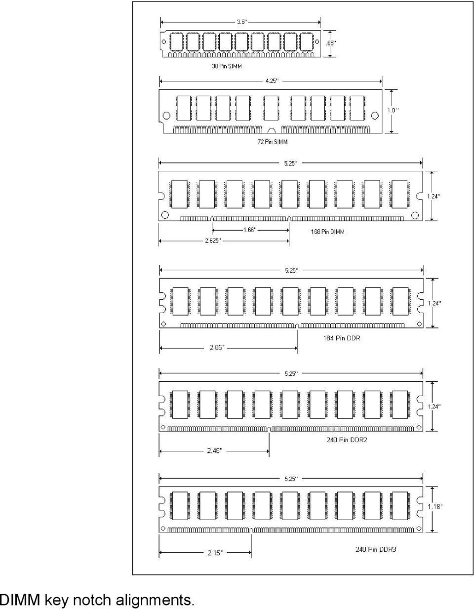
7 RAM, the computer BIOS must be reset thus allowing the SPD to automatically reconfigure the BIOS RAM configuration correctly. Memory Key Notch Alignment Look at the various memory module physical designs in the drawing below. Pay particular attention to DDR1, DDR2, and DDR3 memory module key notch alignment located along the bottom edge of the memory module pins. The key or notch is used to match the proper memory module to the motherboard RAM memory socket. Insertion of the wrong memory module into the motherboard RAM socket will result in damage to the RAM socket. Do not force the memory module into the socket. It should fit snuggly, but experience only a little physical resistance. You can check the motherboard documentation for the correct memory type that is compatible with the motherboard and motherboard chip set. You cannot upgrade DDR1 to DDR2 or DDR2 to DDR3. They are not compatible physically or electrically. DDR is 2.5 Volts, DDR2 is 1.8 and DDR3 is 1.5 Volt. Be aware that some manufacturers may use a slightly different voltage level for their memory module.

8 DIMM key notch alignments.
Random Access Memory (RAM) Types of RAM. RAM Random Access Memory Jamie Tees SDRAM. Micro-DIMM SO-DIMM
 Types of RAM. RAM Random Access Memory Jamie Tees SDRAM. Micro-DIMM SO-DIMM") Random Access Memory (RAM) Sends/Receives data quickly between CPU This is way quicker than using just the HDD RAM holds temporary data used by any open application or active / running process Multiple
Random Access Memory (RAM) Sends/Receives data quickly between CPU This is way quicker than using just the HDD RAM holds temporary data used by any open application or active / running process Multiple
DDR4 Memory Technology on HP Z Workstations
 Technical white paper DDR4 Memory Technology on HP Z Workstations DDR4 is the latest memory technology available for main memory on mobile, desktops, workstations, and server computers. DDR stands for
Table 1: Address Table
 DDR SDRAM DIMM D32PB12C 512MB D32PB1GJ 1GB For the latest data sheet, please visit the Super Talent Electronics web site: www.supertalentmemory.com Features 184-pin, dual in-line memory module (DIMM) Fast
Configuring Memory on the HP Business Desktop dx5150
 Configuring Memory on the HP Business Desktop dx5150 Abstract... 2 Glossary of Terms... 2 Introduction... 2 Main Memory Configuration... 3 Single-channel vs. Dual-channel... 3 Memory Type and Speed...
Intel 965 Express Chipset Family Memory Technology and Configuration Guide
 Intel 965 Express Chipset Family Memory Technology and Configuration Guide White Paper - For the Intel 82Q965, 82Q963, 82G965 Graphics and Memory Controller Hub (GMCH) and Intel 82P965 Memory Controller
Intel Extreme Memory Profile (Intel XMP) DDR3 Technology
 DDR3 Technology") Intel Extreme Memory Profile (Intel XMP) DDR3 Technology White Paper January 2009 Document Number: 319124-002 INFORMATION IN THIS DOCUMENT IS PROVIDED IN CONNECTION WITH INTEL PRODUCTS. NO LICENSE, EXPRESS
Intel Extreme Memory Profile (Intel XMP) DDR3 Technology White Paper January 2009 Document Number: 319124-002 INFORMATION IN THIS DOCUMENT IS PROVIDED IN CONNECTION WITH INTEL PRODUCTS. NO LICENSE, EXPRESS
RAM. Overview DRAM. What RAM means? DRAM
 Overview RAM In this chapter, you will learn how to Identify the different types of RAM packaging Explain the varieties of DRAM Install RAM properly Perform basic RAM troubleshooting Program Execution
Features. DDR SODIMM Product Datasheet. Rev. 1.0 Oct. 2011
 Features 200pin, unbuffered small outline dual in-line memory module (SODIMM) Fast data transfer rates: PC-2100, PC-2700, PC3-3200 Single or Dual rank 256MB(32Megx64), 512MB (64Meg x 64), 1GB(128 Meg x
Computer Architecture
 Computer Architecture Random Access Memory Technologies 2015. április 2. Budapest Gábor Horváth associate professor BUTE Dept. Of Networked Systems and Services ghorvath@hit.bme.hu 2 Storing data Possible
Byte Ordering of Multibyte Data Items
 Byte Ordering of Multibyte Data Items Most Significant Byte (MSB) Least Significant Byte (LSB) Big Endian Byte Addresses +0 +1 +2 +3 +4 +5 +6 +7 VALUE (8-byte) Least Significant Byte (LSB) Most Significant
ThinkServer PC3-10600 DDR3 1333MHz UDIMM and RDIMM PC3-8500 DDR3 1066MHz RDIMM options for the next generation of ThinkServer systems TS200 and RS210
 Hardware Announcement ZG09-0894, dated vember 24, 2009 ThinkServer PC3-10600 DDR3 1333MHz UDIMM and RDIMM PC3-8500 DDR3 1066MHz RDIMM options for the next generation of ThinkServer systems TS200 and RS210
A+ Guide to Managing and Maintaining Your PC, 7e. Chapter 1 Introducing Hardware
 A+ Guide to Managing and Maintaining Your PC, 7e Chapter 1 Introducing Hardware Objectives Learn that a computer requires both hardware and software to work Learn about the many different hardware components
Intel X38 Express Chipset Memory Technology and Configuration Guide
 Intel X38 Express Chipset Memory Technology and Configuration Guide White Paper January 2008 Document Number: 318469-002 INFORMATION IN THIS DOCUMENT IS PROVIDED IN CONNECTION WITH INTEL PRODUCTS. NO LICENSE,
Intel Q35/Q33, G35/G33/G31, P35/P31 Express Chipset Memory Technology and Configuration Guide
 Intel Q35/Q33, G35/G33/G31, P35/P31 Express Chipset Memory Technology and Configuration Guide White Paper August 2007 Document Number: 316971-002 INFORMATION IN THIS DOCUMENT IS PROVIDED IN CONNECTION
The Bus (PCI and PCI-Express)
") 4 Jan, 2008 The Bus (PCI and PCI-Express) The CPU, memory, disks, and all the other devices in a computer have to be able to communicate and exchange data. The technology that connects them is called the
4 Jan, 2008 The Bus (PCI and PCI-Express) The CPU, memory, disks, and all the other devices in a computer have to be able to communicate and exchange data. The technology that connects them is called the
1.55V DDR2 SDRAM FBDIMM
 1.55V DDR2 SDRAM FBDIMM MT18RTF25672FDZ 2GB 2GB (x72, DR) 240-Pin DDR2 SDRAM FBDIMM Features Features 240-pin, fully buffered DIMM (FBDIMM) Very low-power DDR2 operation Component configuration: 256 Meg
White Paper Utilizing Leveling Techniques in DDR3 SDRAM Memory Interfaces
 White Paper Introduction The DDR3 SDRAM memory architectures support higher bandwidths with bus rates of 600 Mbps to 1.6 Gbps (300 to 800 MHz), 1.5V operation for lower power, and higher densities of 2
1. Memory technology & Hierarchy
 1. Memory technology & Hierarchy RAM types Advances in Computer Architecture Andy D. Pimentel Memory wall Memory wall = divergence between CPU and RAM speed We can increase bandwidth by introducing concurrency
Semiconductor Device Technology for Implementing System Solutions: Memory Modules
 Hitachi Review Vol. 47 (1998), No. 4 141 Semiconductor Device Technology for Implementing System Solutions: Memory Modules Toshio Sugano Atsushi Hiraishi Shin ichi Ikenaga ABSTRACT: New technology is producing
DDR3 memory technology
 DDR3 memory technology Technology brief, 3 rd edition Introduction... 2 DDR3 architecture... 2 Types of DDR3 DIMMs... 2 Unbuffered and Registered DIMMs... 2 Load Reduced DIMMs... 3 LRDIMMs and rank multiplication...
A N. O N Output/Input-output connection
 Memory Types Two basic types: ROM: Read-only memory RAM: Read-Write memory Four commonly used memories: ROM Flash, EEPROM Static RAM (SRAM) Dynamic RAM (DRAM), SDRAM, RAMBUS, DDR RAM Generic pin configuration:
Measuring Cache and Memory Latency and CPU to Memory Bandwidth
 White Paper Joshua Ruggiero Computer Systems Engineer Intel Corporation Measuring Cache and Memory Latency and CPU to Memory Bandwidth For use with Intel Architecture December 2008 1 321074 Executive Summary
Dell PowerEdge Servers 2009 - Memory
 Dell PowerEdge Servers 2009 - Memory A Dell Technical White Paper By Paul Benson Dell Enterprise Development February 2009 1 THIS WHITE PAPER IS FOR INFORMATIONAL PURPOSES ONLY, AND MAY CONTAIN TYPOGRAPHICAL
Configuring and using DDR3 memory with HP ProLiant Gen8 Servers
 Engineering white paper, 2 nd Edition Configuring and using DDR3 memory with HP ProLiant Gen8 Servers Best Practice Guidelines for ProLiant servers with Intel Xeon processors Table of contents Introduction
GR2DR4B-EXXX/YYY/LP 1GB & 2GB DDR2 REGISTERED DIMMs (LOW PROFILE)
") GENERAL DESCRIPTION The Gigaram is a 128M/256M bit x 72 DDDR2 SDRAM high density JEDEC standard ECC Registered memory module. The Gigaram consists of eighteen CMOS 128MX4 DDR2 for 1GB and thirty-six CMOS
GENERAL DESCRIPTION The Gigaram is a 128M/256M bit x 72 DDDR2 SDRAM high density JEDEC standard ECC Registered memory module. The Gigaram consists of eighteen CMOS 128MX4 DDR2 for 1GB and thirty-six CMOS
SOLVING HIGH-SPEED MEMORY INTERFACE CHALLENGES WITH LOW-COST FPGAS
 SOLVING HIGH-SPEED MEMORY INTERFACE CHALLENGES WITH LOW-COST FPGAS A Lattice Semiconductor White Paper May 2005 Lattice Semiconductor 5555 Northeast Moore Ct. Hillsboro, Oregon 97124 USA Telephone: (503)
Chapter 5 Cubix XP4 Blade Server
 Chapter 5 Cubix XP4 Blade Server Introduction Cubix designed the XP4 Blade Server to fit inside a BladeStation enclosure. The Blade Server features one or two Intel Pentium 4 Xeon processors, the Intel
Memory Configuration Guide
 Super Micro Computer, Inc. Memory Configuration Guide X9 Socket R Series DP Motherboards Version 1.1R March 12, 2012 Introduction This document is designed to provide the reader with an easy-to-use guide
ADQYF1A08. DDR2-1066G(CL6) 240-Pin O.C. U-DIMM 1GB (128M x 64-bits)
 240-Pin O.C. U-DIMM 1GB (128M x 64-bits)") General Description ADQYF1A08 DDR2-1066G(CL6) 240-Pin O.C. U-DIMM 1GB (128M x 64-bits) The ADATA s ADQYF1A08 is a 128Mx64 bits 1GB DDR2-1066(CL6) SDRAM over clocking memory module, The SPD is programmed
General Description ADQYF1A08 DDR2-1066G(CL6) 240-Pin O.C. U-DIMM 1GB (128M x 64-bits) The ADATA s ADQYF1A08 is a 128Mx64 bits 1GB DDR2-1066(CL6) SDRAM over clocking memory module, The SPD is programmed
Memory Module Specifications KVR667D2D8F5/2GI. 2GB 256M x 72-Bit PC2-5300 CL5 ECC 240-Pin FBDIMM DESCRIPTION SPECIFICATIONS
 Memory Module Specifications KVR667DD8F5/GI GB 56M x 7-Bit PC-5300 CL5 ECC 40- FBDIMM DESCRIPTION This document describes s GB (56M x 7-bit) PC-5300 CL5 (Synchronous DRAM) fully buffered ECC dual rank,
User s Manual HOW TO USE DDR SDRAM
 User s Manual HOW TO USE DDR SDRAM Document No. E0234E30 (Ver.3.0) Date Published April 2002 (K) Japan URL: http://www.elpida.com Elpida Memory, Inc. 2002 INTRODUCTION This manual is intended for users
Computers. Hardware. The Central Processing Unit (CPU) CMPT 125: Lecture 1: Understanding the Computer
 CMPT 125: Lecture 1: Understanding the Computer") Computers CMPT 125: Lecture 1: Understanding the Computer Tamara Smyth, tamaras@cs.sfu.ca School of Computing Science, Simon Fraser University January 3, 2009 A computer performs 2 basic functions: 1.
Computers CMPT 125: Lecture 1: Understanding the Computer Tamara Smyth, tamaras@cs.sfu.ca School of Computing Science, Simon Fraser University January 3, 2009 A computer performs 2 basic functions: 1.
Features. DDR3 SODIMM Product Specification. Rev. 1.7 Feb. 2016
 Features DDR3 functionality and operations supported as defined in the component data sheet 204pin, small-outline dual in-line memory module (SODIMM) Fast data transfer rates: DDR3-1066(PC3-8500) DDR3-1333(PC3-10600)
Memory Module Specifications KVR667D2D4F5/4G. 4GB 512M x 72-Bit PC2-5300 CL5 ECC 240-Pin FBDIMM DESCRIPTION SPECIFICATIONS
 Memory Module Specifications KVR667DD4F5/4G 4GB 5M x 7-Bit PC-5300 CL5 ECC 40- FBDIMM DESCRIPTION This document describes s 4GB (5M x 7-bit) PC-5300 CL5 SDRAM (Synchronous DRAM) fully buffered ECC dual
AMD PhenomII. Architecture for Multimedia System -2010. Prof. Cristina Silvano. Group Member: Nazanin Vahabi 750234 Kosar Tayebani 734923
 AMD PhenomII Architecture for Multimedia System -2010 Prof. Cristina Silvano Group Member: Nazanin Vahabi 750234 Kosar Tayebani 734923 Outline Introduction Features Key architectures References AMD Phenom
CHAPTER 11: Flip Flops
 CHAPTER 11: Flip Flops In this chapter, you will be building the part of the circuit that controls the command sequencing. The required circuit must operate the counter and the memory chip. When the teach
QuickSpecs. Models PC3-10600 (DDR3-1333 MHz) DIMMs
 DIMMs") Overview Models PC3-10600 (DDR3-1333 MHz) DIMMs HP 1-GB PC3-10600 (DDR3-1333 MHz) DIMM HP 2-GB PC3-10600 (DDR3-1333 MHz) DIMM HP 4-GB PC3-10600 (DDR3-1333 MHz) DIMM PC3-10600 (DDR3-1333 MHz) SODIMMs HP
Overview Models PC3-10600 (DDR3-1333 MHz) DIMMs HP 1-GB PC3-10600 (DDR3-1333 MHz) DIMM HP 2-GB PC3-10600 (DDR3-1333 MHz) DIMM HP 4-GB PC3-10600 (DDR3-1333 MHz) DIMM PC3-10600 (DDR3-1333 MHz) SODIMMs HP
MICROPROCESSOR AND MICROCOMPUTER BASICS
 Introduction MICROPROCESSOR AND MICROCOMPUTER BASICS At present there are many types and sizes of computers available. These computers are designed and constructed based on digital and Integrated Circuit
Switch Fabric Implementation Using Shared Memory
 Order this document by /D Switch Fabric Implementation Using Shared Memory Prepared by: Lakshmi Mandyam and B. Kinney INTRODUCTION Whether it be for the World Wide Web or for an intra office network, today
Intel 865G, Intel 865P, Intel 865PE Chipset Memory Configuration Guide
 G, P, PE Chipset Memory Configuration Guide White Paper May 2003 Document Number: 253036-001 INFOMATION IN THIS DOCUMENT IS POVIDED IN CONNECTION WITH INTEL PODUCTS. NO LICENSE, EXPESS O IMPLIED, BY ESTOPPEL
System Installation. 3-1 Socket 370 Celeron/Pentium-III Processor. Installing S370 CPU. Removing CPU. Configuring System Bus
 System Installation This chapter provides you with instructions to set up your system. The additional information is enclosed to help you set up onboard PCI device and handle WDT operation in software
The Motherboard Chapter #5
 The Motherboard Chapter #5 Amy Hissom Key Terms Advanced Transfer Cache (ATC) A type of L2 cache contained within the Pentium processor housing that is embedded on the same core processor die as the CPU
HP 8-GB PC3-12800 (DDR3-1600 MHz) SODIMM
 SODIMM") Overview Models PC3-12800 (DDR3-1600MHz) DIMMs HP 2-GB PC3-12800 (DDR3-1600 MHz) DIMM HP 4-GB PC3-12800 (DDR3-1600 MHz) DIMM HP 8-GB PC3-12800 (DDR3-1600 MHz) DIMM PC3-12800 (DDR3-1600 MHz) SODIMMs HP
Overview Models PC3-12800 (DDR3-1600MHz) DIMMs HP 2-GB PC3-12800 (DDR3-1600 MHz) DIMM HP 4-GB PC3-12800 (DDR3-1600 MHz) DIMM HP 8-GB PC3-12800 (DDR3-1600 MHz) DIMM PC3-12800 (DDR3-1600 MHz) SODIMMs HP
OpenSPARC T1 Processor
 OpenSPARC T1 Processor The OpenSPARC T1 processor is the first chip multiprocessor that fully implements the Sun Throughput Computing Initiative. Each of the eight SPARC processor cores has full hardware
Chapter 6. Inside the System Unit. What You Will Learn... Computers Are Your Future. What You Will Learn... Describing Hardware Performance
 What You Will Learn... Computers Are Your Future Chapter 6 Understand how computers represent data Understand the measurements used to describe data transfer rates and data storage capacity List the components
ThinkServer PC2-5300 DDR2 FBDIMM and PC2-6400 DDR2 SDRAM Memory options boost overall performance of ThinkServer solutions
 , dated September 30, 2008 ThinkServer PC2-5300 DDR2 FBDIMM and PC2-6400 DDR2 SDRAM Memory options boost overall performance of ThinkServer solutions Table of contents 2 Key prerequisites 2 Product number
Technical Product Specifications Dell Dimension 2400 Created by: Scott Puckett
 Technical Product Specifications Dell Dimension 2400 Created by: Scott Puckett Page 1 of 11 Table of Contents Technical Product Specifications Model 3 PC Technical Diagrams Front Exterior Specifications
IBM Europe Announcement ZG08-0232, dated March 11, 2008
 IBM Europe Announcement ZG08-0232, dated March 11, 2008 IBM System x3450 servers feature fast Intel Xeon 2.80 GHz/1600 MHz, 3.0 GHz/1600 MHz, both with 12 MB L2, and 3.4 GHz/1600 MHz, with 6 MB L2 processors,
DDR SDRAM UDIMM MT16VDDT6464A 512MB MT16VDDT12864A 1GB MT16VDDT25664A 2GB
 DDR SDRAM UDIMM MT16VDDT6464A 512MB MT16VDDT12864A 1GB MT16VDDT25664A 2GB For component data sheets, refer to Micron s Web site: www.micron.com 512MB, 1GB, 2GB (x64, DR) 184-Pin DDR SDRAM UDIMM Features
What Every Programmer Should Know About Memory
 What Every Programmer Should Know About Memory Ulrich Drepper Red Hat, Inc. drepper@redhat.com November 21, 2007 1 Introduction Abstract As CPU cores become both faster and more numerous, the limiting
Generations of the computer. processors.
 . Piotr Gwizdała 1 Contents 1 st Generation 2 nd Generation 3 rd Generation 4 th Generation 5 th Generation 6 th Generation 7 th Generation 8 th Generation Dual Core generation Improves and actualizations
Computer Systems Structure Main Memory Organization
 Computer Systems Structure Main Memory Organization Peripherals Computer Central Processing Unit Main Memory Computer Systems Interconnection Communication lines Input Output Ward 1 Ward 2 Storage/Memory
Table 1 SDR to DDR Quick Reference
 TECHNICAL NOTE TN-6-05 GENERAL DDR SDRAM FUNCTIONALITY INTRODUCTION The migration from single rate synchronous DRAM (SDR) to double rate synchronous DRAM (DDR) memory is upon us. Although there are many
QuickSpecs. Models PC3-10600 Memory SODIMMs HP 8 GB PC3-12800 (DDR3 1600 MHz) SODIMM (To be discontinued in 9/30/2013)
 SODIMM (To be discontinued in 9/30/2013)") Models PC3-10600 Memory s HP 2 GB PC3- (To be discontinued in 9/30/2013) HP 4 GB PC3- (To be discontinued in 9/30/2013) HP 8 GB PC3- (To be discontinued in 9/30/2013) HP 2GB DDR3L HP 4GB DDR3L HP 8GB DDR3L
Models PC3-10600 Memory s HP 2 GB PC3- (To be discontinued in 9/30/2013) HP 4 GB PC3- (To be discontinued in 9/30/2013) HP 8 GB PC3- (To be discontinued in 9/30/2013) HP 2GB DDR3L HP 4GB DDR3L HP 8GB DDR3L
Dual DIMM DDR2 and DDR3 SDRAM Interface Design Guidelines
 Dual DIMM DDR2 and DDR3 SDRAM Interface Design Guidelines May 2009 AN-444-1.1 This application note describes guidelines for implementing dual unbuffered DIMM DDR2 and DDR3 SDRAM interfaces. This application
Programming Logic controllers
 Programming Logic controllers Programmable Logic Controller (PLC) is a microprocessor based system that uses programmable memory to store instructions and implement functions such as logic, sequencing,
Server: Performance Benchmark. Memory channels, frequency and performance
 KINGSTON.COM Best Practices Server: Performance Benchmark Memory channels, frequency and performance Although most people don t realize it, the world runs on many different types of databases, all of which
W o r k s h e e t : P r o c e s s o r s
 Time: 1 Hour Revision Date: 6/26/10 Overview This activity is designed to ensure that you understand the topics covered in your courseware. You are required to know the names, purposes and characteristics
Low Power AMD Athlon 64 and AMD Opteron Processors
 Low Power AMD Athlon 64 and AMD Opteron Processors Hot Chips 2004 Presenter: Marius Evers Block Diagram of AMD Athlon 64 and AMD Opteron Based on AMD s 8 th generation architecture AMD Athlon 64 and AMD
Table Of Contents. Page 2 of 26. *Other brands and names may be claimed as property of others.
 Technical White Paper Revision 1.1 4/28/10 Subject: Optimizing Memory Configurations for the Intel Xeon processor 5500 & 5600 series Author: Scott Huck; Intel DCG Competitive Architect Target Audience:
Memory Configuration Guide
 Super Micro Computer, Inc. Memory Configuration Guide X10 Series DP Motherboards (Socket R3) 9/8/2014 Introduction This document is designed to provide the reader with an easy-to-use guide for proper memory
Having read this workbook you should be able to: recognise the arrangement of NAND gates used to form an S-R flip-flop.
 Objectives Having read this workbook you should be able to: recognise the arrangement of NAND gates used to form an S-R flip-flop. describe how such a flip-flop can be SET and RESET. describe the disadvantage
1 Technical Description Lokal-200PC
 1 Technical Description Lokal-200PC 1.1 Overview laptop with in-built accummulator USB connection correlator box internal power supply laptop (if the device has been supplied by F.A.S.T.) BNC aerial connection
Memory unit. 2 k words. n bits per word
 9- k address lines Read n data input lines Memory unit 2 k words n bits per word n data output lines 24 Pearson Education, Inc M Morris Mano & Charles R Kime 9-2 Memory address Binary Decimal Memory contents
DDR2 SDRAM SODIMM MT16HTF12864H 1GB MT16HTF25664H 2GB
 Features DDR2 SDRAM SODIMM MT16HTF12864H 1GB MT16HTF25664H 2GB For component data sheets, refer to Micron s Web site: www.micron.com Features 200-pin, small outline dual in-line memory module (SODIMM)
Decimal Number (base 10) Binary Number (base 2)
 Binary Number (base 2)") LECTURE 5. BINARY COUNTER Before starting with counters there is some vital information that needs to be understood. The most important is the fact that since the outputs of a digital chip can only be
LECTURE 5. BINARY COUNTER Before starting with counters there is some vital information that needs to be understood. The most important is the fact that since the outputs of a digital chip can only be
DDR SDRAM SODIMM. MT9VDDT1672H 128MB 1 MT9VDDT3272H 256MB MT9VDDT6472H 512MB For component data sheets, refer to Micron s Web site: www.micron.
 Features DDR SDRAM SODIMM MT9VDDT1672H 128MB 1 MT9VDDT3272H 256MB MT9VDDT6472H 512MB For component data sheets, refer to Micron s Web site: www.micron.com Features 200-pin, small-outline dual in-line memory
Amplicon Core i5/i7 Ventrix and Impact-R new Systems
 Amplicon Core i5/i7 Ventrix and Impact-R new Systems Tél: 04 37 28 30 34 Fax: 04 37 28 30 39 Email: ventes@ampliconfrance.com What s New? Intel Processor Core i5 / i7 equipped upgrades to Ventrix, Impact-R
DDR SDRAM SODIMM. MT8VDDT3264H 256MB 1 MT8VDDT6464H 512MB For component data sheets, refer to Micron s Web site: www.micron.com
 SODIMM MT8VDDT3264H 256MB 1 MT8VDDT6464H 512MB For component data sheets, refer to Micron s Web site: www.micron.com 256MB, 512MB (x64, SR) 200-Pin SODIMM Features Features 200-pin, small-outline dual
150127-Microprocessor & Assembly Language
 Chapter 3 Z80 Microprocessor Architecture The Z 80 is one of the most talented 8 bit microprocessors, and many microprocessor-based systems are designed around the Z80. The Z80 microprocessor needs an
Unit A451: Computer systems and programming. Section 2: Computing Hardware 1/5: Central Processing Unit
 Unit A451: Computer systems and programming Section 2: Computing Hardware 1/5: Central Processing Unit Section Objectives Candidates should be able to: (a) State the purpose of the CPU (b) Understand the
Tested product: Auslogics BoostSpeed
 Software Tested Tested product: Auslogics BoostSpeed www.softwaretested.com CONTENTS 1 Contents Background... 3 Purpose of the Tests... 5 Testing Environment... 6 Test Results... 10 Windows Startup Time...
CHAPTER 2: HARDWARE BASICS: INSIDE THE BOX
 CHAPTER 2: HARDWARE BASICS: INSIDE THE BOX Multiple Choice: 1. Processing information involves: A. accepting information from the outside world. B. communication with another computer. C. performing arithmetic
Computer Performance. Topic 3. Contents. Prerequisite knowledge Before studying this topic you should be able to:
 55 Topic 3 Computer Performance Contents 3.1 Introduction...................................... 56 3.2 Measuring performance............................... 56 3.2.1 Clock Speed.................................
Embedded Multi-Media Card Specification (e MMC 4.5)
") Product Features: Packaged NAND flash memory with e MMC 4.5 interface Compliant with e MMC Specification Ver 4.41 & 4.5. Bus mode - High-speed e MMC protocol - Provide variable clock frequencies
Product Features: Packaged NAND flash memory with e MMC 4.5 interface Compliant with e MMC Specification Ver 4.41 & 4.5. Bus mode - High-speed e MMC protocol - Provide variable clock frequencies
Features. DDR3 Unbuffered DIMM Spec Sheet
 Features DDR3 functionality and operations supported as defined in the component data sheet 240-pin, unbuffered dual in-line memory module (UDIMM) Fast data transfer rates: PC3-8500, PC3-10600, PC3-12800
DDR subsystem: Enhancing System Reliability and Yield
 DDR subsystem: Enhancing System Reliability and Yield Agenda Evolution of DDR SDRAM standards What is the variation problem? How DRAM standards tackle system variability What problems have been adequately
Homework # 2. Solutions. 4.1 What are the differences among sequential access, direct access, and random access?
 ECE337 / CS341, Fall 2005 Introduction to Computer Architecture and Organization Instructor: Victor Manuel Murray Herrera Date assigned: 09/19/05, 05:00 PM Due back: 09/30/05, 8:00 AM Homework # 2 Solutions
x64 Servers: Do you want 64 or 32 bit apps with that server?
 TMurgent Technologies x64 Servers: Do you want 64 or 32 bit apps with that server? White Paper by Tim Mangan TMurgent Technologies February, 2006 Introduction New servers based on what is generally called
AVR151: Setup and Use of the SPI. Introduction. Features. Atmel AVR 8-bit Microcontroller APPLICATION NOTE
 Atmel AVR 8-bit Microcontroller AVR151: Setup and Use of the SPI APPLICATION NOTE Introduction This application note describes how to set up and use the on-chip Serial Peripheral Interface (SPI) of the
Chapter 4 System Unit Components. Discovering Computers 2012. Your Interactive Guide to the Digital World
 Chapter 4 System Unit Components Discovering Computers 2012 Your Interactive Guide to the Digital World Objectives Overview Differentiate among various styles of system units on desktop computers, notebook
DDR3 DIMM Slot Interposer
 DDR3 DIMM Slot Interposer DDR3-1867 Digital Validation High Speed DDR3 Digital Validation Passive 240-pin DIMM Slot Interposer Custom Designed for Agilent Logic Analyzers Compatible with Agilent Software
Technical Information Jumpers, Connectors and Memory JXM7031 (7031-xxx) MicroATX Motherboard Dual Jasper Forest Processors
 MicroATX Motherboard Dual Jasper Forest Processors") Technical Information Jumpers, Connectors and Memory JXM7031 (7031-xxx) MicroATX Motherboard Dual Jasper Forest Processors Dimension Diagram * = Pin 1 = Card Slots are on.800 centers Notes: All dimensions
Technical Information Jumpers, Connectors and Memory JXM7031 (7031-xxx) MicroATX Motherboard Dual Jasper Forest Processors Dimension Diagram * = Pin 1 = Card Slots are on.800 centers Notes: All dimensions
Building A Computer: A Beginners Guide
 Building A Computer: A Beginners Guide Mr. Marty Brandl The following was written to help an individual setup a Pentium 133 system using an ASUS P/I- P55T2P4 motherboard. The tutorial includes the installation
PCI Express IO Virtualization Overview
 Ron Emerick, Oracle Corporation Author: Ron Emerick, Oracle Corporation SNIA Legal Notice The material contained in this tutorial is copyrighted by the SNIA unless otherwise noted. Member companies and
Chapter 5 :: Memory and Logic Arrays
 Chapter 5 :: Memory and Logic Arrays Digital Design and Computer Architecture David Money Harris and Sarah L. Harris Copyright 2007 Elsevier 5- ROM Storage Copyright 2007 Elsevier 5- ROM Logic Data
Memory technology evolution: an overview of system memory technologies
 Memory technology evolution: an overview of system memory technologies Technology brief, 9 th edition Introduction... 2 Basic DRAM operation... 2 DRAM storage density and power consumption... 4 Memory
Chapter 13. PIC Family Microcontroller
 Chapter 13 PIC Family Microcontroller Lesson 01 PIC Characteristics and Examples PIC microcontroller characteristics Power-on reset Brown out reset Simplified instruction set High speed execution Up to
Dell Reliable Memory Technology
 Dell Reliable Memory Technology Detecting and isolating memory errors THIS WHITE PAPER IS FOR INFORMATIONAL PURPOSES ONLY, AND MAY CONTAIN TYPOGRAPHICAL ERRORS AND TECHNICAL INACCURACIES. THE CONTENT IS
Version 3.0 Technical Brief
 Version 3.0 Technical Brief Release 1.0 May 15, 2008 Document Change History Ver Date Resp Reason for change 1 May 15, 2008 GG, LB, AT Initial revision. ii Introduction The Mobile PCI Express Module (MXM)
DDR2 SDRAM SODIMM MT8HTF3264HD 256MB MT8HTF6464HD 512MB MT8HTF12864HD 1GB For component data sheets, refer to Micron s Web site: www.micron.
 DDR2 SDRAM SODIMM MT8HTF3264HD 256MB MT8HTF6464HD 512MB MT8HTF12864HD 1GB For component data sheets, refer to Micron s Web site: www.micron.com 256MB, 512MB, 1GB (x64, DR): 200-Pin DDR2 SODIMM Features
AMD Opteron Quad-Core
 AMD Opteron Quad-Core a brief overview Daniele Magliozzi Politecnico di Milano Opteron Memory Architecture native quad-core design (four cores on a single die for more efficient data sharing) enhanced
Technical Note. Initialization Sequence for DDR SDRAM. Introduction. Initializing DDR SDRAM
 TN-46-8: Initialization Sequence for DDR SDRAM Introduction Technical Note Initialization Sequence for DDR SDRAM Introduction The double data rate DDR synchronous dynamic random access memory SDRAM device
Understanding PCI Bus, PCI-Express and In finiband Architecture
 White Paper Understanding PCI Bus, PCI-Express and In finiband Architecture 1.0 Overview There is some confusion in the market place concerning the replacement of the PCI Bus (Peripheral Components Interface)
The Central Processing Unit:
 The Central Processing Unit: What Goes on Inside the Computer Chapter 4 Objectives Identify the components of the central processing unit and how they work together and interact with memory Describe how
Communicating with devices
 Introduction to I/O Where does the data for our CPU and memory come from or go to? Computers communicate with the outside world via I/O devices. Input devices supply computers with data to operate on.
Understanding Memory TYPES OF MEMORY
 Understanding Memory TYPES OF MEMORY In this study unit, you ll learn about physical and logical memory. Physical memory comes in two types, random access memory (RAM) and read-only memory (ROM). Typically,
Address Summary Table: 128MB 256MB 512MB 1GB 2GB Module
 12MB - WD1SN12X0 256MB - WD1SN256X0 512MB - WD1SN512X0 1GB - WD1SN01GX0 2GB - WD1SN02GS0 (Stacked) Features: 200-pin Unbuffered Non-ECC DDR SDRAM SODIMM for DDR-266, DDR-333, DDR-400 JEDEC standard VDD=2.5V
Logical Operations. Control Unit. Contents. Arithmetic Operations. Objectives. The Central Processing Unit: Arithmetic / Logic Unit.
 Objectives The Central Processing Unit: What Goes on Inside the Computer Chapter 4 Identify the components of the central processing unit and how they work together and interact with memory Describe how
Samsung DDR4 SDRAM DDR4 SDRAM
 Samsung DDR4 SDRAM The new generation of high-performance, power-efficient memory that delivers greater reliability for enterprise applications DDR4 SDRAM An optimized memory for enterprise-level workloads