Measuring Metastability
|
|
|
- Jasmine Marsh
- 7 years ago
- Views:
Transcription
1 Measuring Metastability Sandeep Mandarapu Department of Electrical and Computer Engineering, VLSI Design Research Laboratory, Southern Illinois University Edwardsville, Illinois, USA, ECE595: Masters Project Abstract Digital circuits can exhibit metastable behavior when there are setup and hold time violations in the circuits. This paper describes the experimental method to detect metastability behavior of a flip-flop [1] and a circuit to measure the delay in the data path. We used a master-slave D flip-flop to observe the metastability and tried to observe the metastability behavior with both digital IC s and an FPGA. We developed a PCB layout for the PCB board for the metastability detection circuit. 1.0 Introduction Theoretical study and experimental research have confirmed that digital circuits can exhibit metastable behavior when the input to the flip-flop is asynchronous to the system clock. When an asynchronous input violates the setup and hold times of the flip-flop, the resulting metasatble state can cause oscillatory behavior in the output of the flip-flop. Generally metastability measurements make use of two asynchronous oscillators driving the D and Clock inputs of a master-slave flip-flop. Here we used a
![This paper describes the experimental method to detect metastability behavior of a flip-flop [1] and a circuit to measure the delay in the data path.](/docs-images/46/21624707/images/page_1.jpg "We used a master-slave D flip-flop to observe the metastability and tried to observe the metastability behavior with both digital IC s and an FPGA.")
2 single clock, which drives both the clock and data lines. We used a separate input to the data path to increase the delay. If the data oscillator has a period of 99.9 ns, the clock oscillator has 100ns and the set up + hold time is 100ps, the rising clock edge may, or may not produce a change in the output Q. When the D input changes in the critical window (set up + hold time) the output Q enters a state where its value is unpredictable. Fig.1 shows the situation when the D input is low in the first rising clock edge then goes high very close to the next rising clock edge causing metastability to occur. To observe the delay due to metastability, the Q change from low to high is used to trigger the recording of each clock rising edge for a potentially metastable event [1]. Fig.1 - Two- oscillator metastability measurement The rate of generation of metastable events can be calculated by taking the ratio of the setup and hold time window to the time between clock edges and multiplying with the data edge frequency [3]. This generation rate of metastable events coupled with the probability of non-resolution of an event as a function of the time allowed for resolution

3 gives the failure rate for that set of conditions. The inverse of the failure rate is the mean time between failures (MTBF). MTBF is mean time between failures, it gives us information on how often a particular element will fail or it gives the average time interval between two successive failures [1][5]. MTBF=e (t / τ ) / T w f c f d f c Is the clock frequency f d data transition frequency T w Metastability window t is the amount of time required by the synchronizer for long term reliability and τ is the resolving time constant of the synchronizer. The assumption implicit in the MTBF formula is that on average an input transition t from the balance point, that is the input time where resolution of metastability takes the longest [1], is given by t = 1/ f c f d MTBF. t = τ. ln (T w / t)

4 2.0 Measuring Delay: A schematic of the test set-up is shown in Fig.2. Here a 4MHz clock is passed through two closely matched paths to the data and clock inputs of the device under test. We used an external control voltagev3 in data path. Adjusting the control voltage to the open collector inverters varies the delay in the path to the data input. If the data rising edge is slightly slow when compared to the clock edge, Q will be low. If the data rising edge is fast, Q will be high. Fig.2 - Test schematic

5 For this test we used 74ALS05 for open collector inverters and 74F04 for the general inverters. For the device under test we used 74F74, a master-slave flip-flop specially designed to give a fast, controlled metastability response. We used an oscilloscope for observing the Q output. In the test procedure we used an external control voltage V3 in data path. Delay in the clock path is fixed. We varied the control voltage V3 in the data path and observed the output Q. We tested this schematic with 5V Vcc and 3.3V Vcc. With the circuit with a 5V Vcc, if we increase the supply voltage to 2.5V, the data comes as early as 5ns. If we increase it to 3.5V, data comes at the time when clock comes. If we further increase the supply voltage to 4.5V, data comes 5ns late. With 5V Vcc circuit if we increase the control voltage V3 from 0 to 5V, the delay in the data path varies by +/- 5ns,. Fig.3 5V Vcc, Control voltage V3 2.5V Delay --- 5ns

6 Fig.4-5V Vcc, Control voltage V3 3.5V delay --- 0ns Fig.5-5V Vcc, Control voltage V3 4V delay --- 4ns We changed the resistor values in the data path and varied the control voltage V3 to observe the delay. The resistor values we used are 470 ohms, 680 ohms, 820 ohms. The respective delays are shown in Table1 and Table 2.

7 470 ohms(+5v Vcc) 680 ohms (+5V Vcc) Voltage(V) Delay (ns) Voltage(V) Delay(ns) Table ohms (+5V Vcc) 820 ohms (+3.3V Vcc) Voltage (V) Delay (ns) Voltage (V) Delay (ns) Table 2 With the circuit with 3.3V Vcc, if we increase the control voltagev3 to 1.8V the data comes as early as 4ns. If we increase it to 2.9V, data and clock come at the same time. If we further increase the control voltagev3 to 4V data comes 4ns late. With 3.3V Vcc circuit if we increase the control voltage V3 from 0 to 5V, the delay in the data path varies by +/- 4ns.

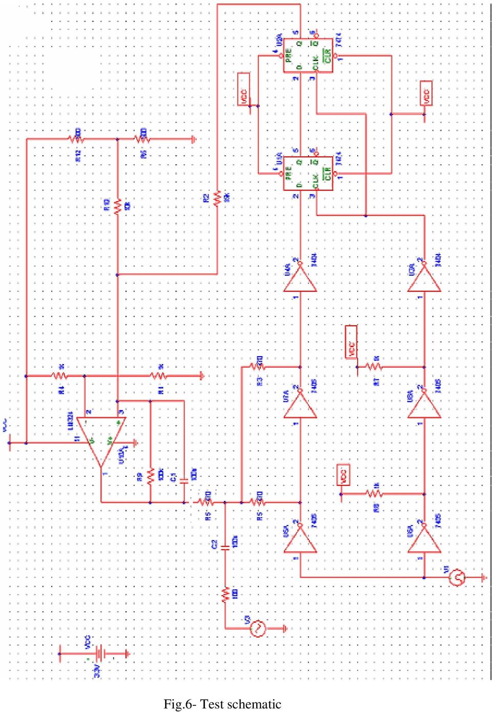
8 2.1 Measuring metastability: A schematic of the test setup is shown in Fig.6. Here a 4MHz clock is passed through two closely matched paths to the data and clock inputs of the master-slave flip-flop. We adjusted the supply voltage to open collector inverters, which varied the delay in the data path. If the data rising edge is slightly slow when compared to the clock edge, Q will be low. If it is fast, Q will be high. A slave flip-flop records whether the device under test has resolved high or low, and an analog integrator is used to average the proportion of high to low outputs from the slave [1]. This arrangement forms a delay locked loop in which the voltage supply to the inverters in the data path is increased if it is too slow and reduced if it is too fast. The integrator has a second input that enables the proportion of highs and lows to be set manually, normally we set the input voltage to vhigh+vlow/2 so that the system settles to a steady state where 50% of the flip-flop outputs are high and 50% are low but it is possible to vary the proportions simply by increasing or reducing the proportion of high slave outputs, and vice versa [1]. We used an LM324 for the integrator. We used an external control voltage V3 with frequency 15MHz in the data path to enable a highspeed waveform to vary the delay around + or 100ns. We tested this schematic with both +5V Vcc and +3.3V Vcc, because FPGA runs at +3.3V Vcc.

9 Fig.6- Test schematic
10 We varied the external control voltagev3 and observed the output Q in oscilloscope. There is a metastability occurrence from 1.5V to 2.5V. The results are shown in Fig.7 and Fig.8. In Fig.7 and Fig.8 the master flip-flop is taking 6ns to resolve to either high or low. Fig.7 Master Flip-flop output when control voltage V3 is 1.5v and frequency is 15MHz Fig.8 Master flip-flop output when control voltage V3 is 2.5v and frequency is 15MHz

11 We used a 74HC04 for the general inverters and a 74HC74 for the D flip-flop in +3.3 Vcc circuit, because they are compatible with the +3.3Vcc. There is a metastability occurrence from 0.7V to 2V. We observed the output using an Agilent technologies infinium oscilloscope. The corresponding results are shown in Fig.9 and Fig.10. In Fig.10 the master flip-flop is taking 10ns to resolve to either high or low. In Fig.11 the master flip-flop is taking 20ns to resolve to either high or low. Fig 9 Master flip-flop output when control voltage V3 is 1V and frequency is 15MHz Fig 10 Master flip-flop output when control voltage V3 is 1.8V and frequency is 15MHz

12 2.2 Measuring Metastability with FPGA: In this test procedure we used verilog code for the metastable master slave flip-flop. We synthesized the verilog code in Xilinx. It generated a programming file for the XSA board as.bit file. We then programmed the XSA board using the GXS tools. The test schematic is shown below. Fig11 Test schematic with FPGA

13 In the synthesis using Xilinx we did not put I/O buffers and we turned off the register packing into I/O s. After that we created a UCF file, in that we used pin 15 for clock, pin 84 for data, pin86 for the master flip-flop output and pin 85 for the slave output. In the test schematic we used a 74HC04 for the general inverters and a 74HC74 for the D flip-flop. We changed the Vcc to +3.3V. As the FPGA s have setup and hold time of around very few ns, we were not able to make the data change in that window. As a result of that we could not see any metastability behavior using FPGA s. Even if the data is having a delay of +/- 7ns, we could not see any metastability behavior at the master flip-flop output. Fig 12 Master flip-flop output when control voltage V3 is 1.5v and frequency is 15MHz

14 2.3 PCB Layout: We developed the PCB layout for the test schematic using Eagle layout editor 4.16r2. The layout is shown in Fig.13. We used a connector to connect the PCB layout with XS board. The connector we used is 0.5mm pitch, 2.5mm above the board, flexible flat cable ZIF connector. Fig.13 PCB layout for the test schematic

15 3.0 Summary: With the circuit presented in this paper we measured the delay in the data path. We were able to observe the metastable behavior of the master-slave D flip-flop using the test schematic [1] presented in this paper. When the D input changes in the critical window (setup + hold time) the master flip-flop output enters a state where its value is unpredictable. We could see the metastability with circuits having +5V Vcc and +3.3V Vcc. With the circuit having +5V vdd the master flip-flop has taken 6ns to resolve to either high or low. With the circuit having +3.3V vdd the master flip-flop has taken 20ns to resolve to either high or low. When we tested for metastability using FPGA s we could not see any metastable behavior because the setup and hold time window is very small and is in the order of very few ns. We developed the PCB layout for the PCB board for the metastability detection circuit.

16 References: 1. Measuring Deep Metastability, David Kinniment, Keith Heron, and Gordon Russell New castle university, UK, pp1,2,3. 2. Metastability Performance of Clocked FIFOs, First-In, First-Out Technology, Chris Wellheuser, Advanced System Logic Semiconductor Group, pp1. 3. Evaluating Metastability in Electronic Circuits for Random Number Generation, ShondaWalker and SimonFoo Department of Electrical Engineering FAMU-FSU College of Engineering Tallahassee, FL, USA, pp1 4. J. M. Rabaey, A. Chandrakasan, B. Nikolic, Digital Integrated Circuits, Prentice Hall, 2003, pp Neil H.E. Weste, Kamran Eshraghian, PRINCIPLES OF CMOS VLSI DESIGN, Addison Wesley, 1992, pp339, 340.

17 Appendix: Verilog code for the metastable master-slave D flip-flop. `timescale 1ns / 1ps module ms(clk, data, qm, qs); input clk; input data; output qm; output qs; FD XLXI_1 (.C(clk),.D(data),.Q(qm)); defparam XLXI_1.INIT = 1'b0; FD XLXI_2 (.C(clk),.D(qm),.Q(qs)); defparam XLXI_2.INIT = 1'b0; endmodule
,.D(qm),.Q(qs)); defparam XLXI_2.")
Master/Slave Flip Flops
 Master/Slave Flip Flops Page 1 A Master/Slave Flip Flop ( Type) Gated latch(master) Gated latch (slave) 1 Gate Gate GATE Either: The master is loading (the master in on) or The slave is loading (the slave
Sequential Logic: Clocks, Registers, etc.
 ENEE 245: igital Circuits & Systems Lab Lab 2 : Clocks, Registers, etc. ENEE 245: igital Circuits and Systems Laboratory Lab 2 Objectives The objectives of this laboratory are the following: To design
Latches, the D Flip-Flop & Counter Design. ECE 152A Winter 2012
 Latches, the D Flip-Flop & Counter Design ECE 52A Winter 22 Reading Assignment Brown and Vranesic 7 Flip-Flops, Registers, Counters and a Simple Processor 7. Basic Latch 7.2 Gated SR Latch 7.2. Gated SR
PLL frequency synthesizer
 ANALOG & TELECOMMUNICATION ELECTRONICS LABORATORY EXERCISE 4 Lab 4: PLL frequency synthesizer 1.1 Goal The goals of this lab exercise are: - Verify the behavior of a and of a complete PLL - Find capture
EE552. Advanced Logic Design and Switching Theory. Metastability. Ashirwad Bahukhandi. (Ashirwad Bahukhandi) bahukhan@usc.edu
 bahukhan@usc.edu") EE552 Advanced Logic Design and Switching Theory Metastability by Ashirwad Bahukhandi (Ashirwad Bahukhandi) bahukhan@usc.edu This is an overview of what metastability is, ways of interpreting it, the issues
EE552 Advanced Logic Design and Switching Theory Metastability by Ashirwad Bahukhandi (Ashirwad Bahukhandi) bahukhan@usc.edu This is an overview of what metastability is, ways of interpreting it, the issues
Clocking. Figure by MIT OCW. 6.884 - Spring 2005 2/18/05 L06 Clocks 1
 ing Figure by MIT OCW. 6.884 - Spring 2005 2/18/05 L06 s 1 Why s and Storage Elements? Inputs Combinational Logic Outputs Want to reuse combinational logic from cycle to cycle 6.884 - Spring 2005 2/18/05
Sequential Logic Design Principles.Latches and Flip-Flops
 Sequential Logic Design Principles.Latches and Flip-Flops Doru Todinca Department of Computers Politehnica University of Timisoara Outline Introduction Bistable Elements Latches and Flip-Flops S-R Latch
White Paper Understanding Metastability in FPGAs
 White Paper Understanding Metastability in FPGAs This white paper describes metastability in FPGAs, why it happens, and how it can cause design failures. It explains how metastability MTBF is calculated,
Timing Methodologies (cont d) Registers. Typical timing specifications. Synchronous System Model. Short Paths. System Clock Frequency
 Registers. Typical timing specifications. Synchronous System Model. Short Paths. System Clock Frequency") Registers Timing Methodologies (cont d) Sample data using clock Hold data between clock cycles Computation (and delay) occurs between registers efinition of terms setup time: minimum time before the clocking
Registers Timing Methodologies (cont d) Sample data using clock Hold data between clock cycles Computation (and delay) occurs between registers efinition of terms setup time: minimum time before the clocking
POCKET SCOPE 2. The idea 2. Design criteria 3
 POCKET SCOPE 2 The idea 2 Design criteria 3 Microcontroller requirements 3 The microcontroller must have speed. 3 The microcontroller must have RAM. 3 The microcontroller must have secure Flash. 3 The
A Lesson on Digital Clocks, One Shots and Counters
 A Lesson on Digital Clocks, One Shots and Counters Topics Clocks & Oscillators LM 555 Timer IC Crystal Oscillators Selection of Variable Resistors Schmitt Gates Power-On Reset Circuits One Shots Counters
The enable pin needs to be high for data to be fed to the outputs Q and Q bar.
 of 7 -Type flip-flop (Toggle switch) The -type flip-flops are used in prescalar/divider circuits and frequency phase detectors. Figure shows how the flip-flop (latch) can be made using -input logic circuits
A Lesson on Digital Clocks, One Shots and Counters
 A Lesson on Digital Clocks, One Shots and Counters Topics Clocks & Oscillators LM 555 Timer IC Crystal Oscillators Selection of Variable Resistors Schmitt Gates Power-On Reset Circuits One Shots Counters
PROGETTO DI SISTEMI ELETTRONICI DIGITALI. Digital Systems Design. Digital Circuits Advanced Topics
 PROGETTO DI SISTEMI ELETTRONICI DIGITALI Digital Systems Design Digital Circuits Advanced Topics 1 Sequential circuit and metastability 2 Sequential circuit - FSM A Sequential circuit contains: Storage
EE 459/500 HDL Based Digital Design with Programmable Logic. Lecture 16 Timing and Clock Issues
 EE 459/500 HDL Based Digital Design with Programmable Logic Lecture 16 Timing and Clock Issues 1 Overview Sequential system timing requirements Impact of clock skew on timing Impact of clock jitter on
Low latency synchronization through speculation
 Low latency synchronization through speculation D.J.Kinniment, and A.V.Yakovlev School of Electrical and Electronic and Computer Engineering, University of Newcastle, NE1 7RU, UK {David.Kinniment,Alex.Yakovlev}@ncl.ac.uk
L4: Sequential Building Blocks (Flip-flops, Latches and Registers)
") L4: Sequential Building Blocks (Flip-flops, Latches and Registers) Acknowledgements: Materials in this lecture are courtesy of the following sources and are used with permission. Prof. Randy Katz (Unified
L4: Sequential Building Blocks (Flip-flops, Latches and Registers) Acknowledgements: Materials in this lecture are courtesy of the following sources and are used with permission. Prof. Randy Katz (Unified
Fairchild Solutions for 133MHz Buffered Memory Modules
 AN-5009 Fairchild Semiconductor Application Note April 1999 Revised December 2000 Fairchild Solutions for 133MHz Buffered Memory Modules Fairchild Semiconductor provides several products that are compatible
Experiment # 9. Clock generator circuits & Counters. Eng. Waleed Y. Mousa
 Experiment # 9 Clock generator circuits & Counters Eng. Waleed Y. Mousa 1. Objectives: 1. Understanding the principles and construction of Clock generator. 2. To be familiar with clock pulse generation
Introduction to CMOS VLSI Design (E158) Lecture 8: Clocking of VLSI Systems
 Lecture 8: Clocking of VLSI Systems") Harris Introduction to CMOS VLSI Design (E158) Lecture 8: Clocking of VLSI Systems David Harris Harvey Mudd College David_Harris@hmc.edu Based on EE271 developed by Mark Horowitz, Stanford University MAH
Harris Introduction to CMOS VLSI Design (E158) Lecture 8: Clocking of VLSI Systems David Harris Harvey Mudd College David_Harris@hmc.edu Based on EE271 developed by Mark Horowitz, Stanford University MAH
Set-Reset (SR) Latch
 Latch") et-eset () Latch Asynchronous Level sensitive cross-coupled Nor gates active high inputs (only one can be active) + + Function 0 0 0 1 0 1 eset 1 0 1 0 et 1 1 0-? 0-? Indeterminate cross-coupled Nand gates
et-eset () Latch Asynchronous Level sensitive cross-coupled Nor gates active high inputs (only one can be active) + + Function 0 0 0 1 0 1 eset 1 0 1 0 et 1 1 0-? 0-? Indeterminate cross-coupled Nand gates
STUDY OF CELLPHONE CHARGERS
 STUDY OF CELLPHONE CHARGERS Author : Suraj Hebbar Systems Lab, CeNSE,IISc Banglore ABSTRACT This report shows charging nature of different cellphone chargers with different cellphones. Here we took into
Lecture-3 MEMORY: Development of Memory:
 Lecture-3 MEMORY: It is a storage device. It stores program data and the results. There are two kind of memories; semiconductor memories & magnetic memories. Semiconductor memories are faster, smaller,
CHAPTER 11: Flip Flops
 CHAPTER 11: Flip Flops In this chapter, you will be building the part of the circuit that controls the command sequencing. The required circuit must operate the counter and the memory chip. When the teach
Modeling Sequential Elements with Verilog. Prof. Chien-Nan Liu TEL: 03-4227151 ext:34534 Email: jimmy@ee.ncu.edu.tw. Sequential Circuit
 Modeling Sequential Elements with Verilog Prof. Chien-Nan Liu TEL: 03-4227151 ext:34534 Email: jimmy@ee.ncu.edu.tw 4-1 Sequential Circuit Outputs are functions of inputs and present states of storage elements
LM 358 Op Amp. If you have small signals and need a more useful reading we could amplify it using the op amp, this is commonly used in sensors.
 LM 358 Op Amp S k i l l L e v e l : I n t e r m e d i a t e OVERVIEW The LM 358 is a duel single supply operational amplifier. As it is a single supply it eliminates the need for a duel power supply, thus
INTEGRATED CIRCUITS. For a complete data sheet, please also download:
 INTEGRATED CIRCUITS DATA SEET For a complete data sheet, please also download: The IC6 74C/CT/CU/CMOS ogic Family Specifications The IC6 74C/CT/CU/CMOS ogic Package Information The IC6 74C/CT/CU/CMOS ogic
CSE140: Components and Design Techniques for Digital Systems
 CE4: Components and esign Techniques for igital ystems Tajana imunic osing ources: Where we are now What we ve covered so far (Chap -5, App. A& B) Number representations Boolean algebra OP and PO Logic
INTEGRATED CIRCUITS. For a complete data sheet, please also download:
 INTEGRATED CIRCUITS DATA SEET For a complete data sheet, please also download: The IC6 74C/CT/CU/CMOS Logic Family Specifications The IC6 74C/CT/CU/CMOS Logic Package Information The IC6 74C/CT/CU/CMOS
TRUE SINGLE PHASE CLOCKING BASED FLIP-FLOP DESIGN
 TRUE SINGLE PHASE CLOCKING BASED FLIP-FLOP DESIGN USING DIFFERENT FOUNDRIES Priyanka Sharma 1 and Rajesh Mehra 2 1 ME student, Department of E.C.E, NITTTR, Chandigarh, India 2 Associate Professor, Department
ECE124 Digital Circuits and Systems Page 1
 ECE124 Digital Circuits and Systems Page 1 Chip level timing Have discussed some issues related to timing analysis. Talked briefly about longest combinational path for a combinational circuit. Talked briefly
Latch Timing Parameters. Flip-flop Timing Parameters. Typical Clock System. Clocking Overhead
 Clock - key to synchronous systems Topic 7 Clocking Strategies in VLSI Systems Peter Cheung Department of Electrical & Electronic Engineering Imperial College London Clocks help the design of FSM where
DM74LS169A Synchronous 4-Bit Up/Down Binary Counter
 Synchronous 4-Bit Up/Down Binary Counter General Description This synchronous presettable counter features an internal carry look-ahead for cascading in high-speed counting applications. Synchronous operation
Pmod peripheral modules are powered by the host via the interface s power and ground pins.
 Digilent Pmod Interface Specification Revision: November 20, 2011 1300 NE Henley Court, Suite 3 Pullman, WA 99163 (509) 334 6306 Voice (509) 334 6300 Fax Introduction The Digilent Pmod interface is used
Topics of Chapter 5 Sequential Machines. Memory elements. Memory element terminology. Clock terminology
 Topics of Chapter 5 Sequential Machines Memory elements Memory elements. Basics of sequential machines. Clocking issues. Two-phase clocking. Testing of combinational (Chapter 4) and sequential (Chapter
Flip-Flops and Sequential Circuit Design. ECE 152A Winter 2012
 Flip-Flops and Sequential Circuit Design ECE 52 Winter 22 Reading ssignment Brown and Vranesic 7 Flip-Flops, Registers, Counters and a Simple Processor 7.5 T Flip-Flop 7.5. Configurable Flip-Flops 7.6
Flip-Flops and Sequential Circuit Design
 Flip-Flops and Sequential Circuit Design ECE 52 Winter 22 Reading ssignment Brown and Vranesic 7 Flip-Flops, Registers, Counters and a Simple Processor 7.5 T Flip-Flop 7.5. Configurable Flip-Flops 7.6
ISSCC 2003 / SESSION 13 / 40Gb/s COMMUNICATION ICS / PAPER 13.7
 ISSCC 2003 / SESSION 13 / 40Gb/s COMMUNICATION ICS / PAPER 13.7 13.7 A 40Gb/s Clock and Data Recovery Circuit in 0.18µm CMOS Technology Jri Lee, Behzad Razavi University of California, Los Angeles, CA
INTEGRATED CIRCUITS. For a complete data sheet, please also download:
 INTEGRATED CIRCUITS DATA SEET For a complete data sheet, please also download: The IC6 74C/CT/CU/CMOS ogic Family Specifications The IC6 74C/CT/CU/CMOS ogic Package Information The IC6 74C/CT/CU/CMOS ogic
Flip-Flops, Registers, Counters, and a Simple Processor
 June 8, 22 5:56 vra235_ch7 Sheet number Page number 349 black chapter 7 Flip-Flops, Registers, Counters, and a Simple Processor 7. Ng f3, h7 h6 349 June 8, 22 5:56 vra235_ch7 Sheet number 2 Page number
TESTS OF 1 MHZ SIGNAL SOURCE FOR SPECTRUM ANALYZER CALIBRATION 7/8/08 Sam Wetterlin
 TESTS OF 1 MHZ SIGNAL SOURCE FOR SPECTRUM ANALYZER CALIBRATION 7/8/08 Sam Wetterlin (Updated 7/19/08 to delete sine wave output) I constructed the 1 MHz square wave generator shown in the Appendix. This
DRM compatible RF Tuner Unit DRT1
 FEATURES DRM compatible RF Tuner Unit DRT1 High- Performance RF Tuner Frequency Range: 10 KHz to 30 MHz Input ICP3: +13,5dBm, typ. Noise Figure @ full gain: 14dB, typ. Receiver Factor: -0,5dB, typ. Input
S. Venkatesh, Mrs. T. Gowri, Department of ECE, GIT, GITAM University, Vishakhapatnam, India
 Power reduction on clock-tree using Energy recovery and clock gating technique S. Venkatesh, Mrs. T. Gowri, Department of ECE, GIT, GITAM University, Vishakhapatnam, India Abstract Power consumption of
On-chip clock error characterization for clock distribution system
 On-chip clock error characterization for clock distribution system Chuan Shan, Dimitri Galayko, François Anceau Laboratoire d informatique de Paris 6 (LIP6) Université Pierre & Marie Curie (UPMC), Paris,
Pericom PCI Express 1.0 & PCI Express 2.0 Advanced Clock Solutions
 Pericom PCI Express 1.0 & PCI Express 2.0 Advanced Clock Solutions PCI Express Bus In Today s Market PCI Express, or PCIe, is a relatively new serial pointto-point bus in PCs. It was introduced as an AGP
11. High-Speed Differential Interfaces in Cyclone II Devices
 11. High-Speed Differential Interfaces in Cyclone II Devices CII51011-2.2 Introduction From high-speed backplane applications to high-end switch boxes, low-voltage differential signaling (LVDS) is the
INTEGRATED CIRCUITS. For a complete data sheet, please also download:
 INTEGRATED CIRCUITS DATA SHEET For a complete data sheet, please also download: The IC06 74HC/HCT/HCU/HCMOS ogic Family Specifications The IC06 74HC/HCT/HCU/HCMOS ogic Package Information The IC06 74HC/HCT/HCU/HCMOS
AC 2007-2485: PRACTICAL DESIGN PROJECTS UTILIZING COMPLEX PROGRAMMABLE LOGIC DEVICES (CPLD)
") AC 2007-2485: PRACTICAL DESIGN PROJECTS UTILIZING COMPLEX PROGRAMMABLE LOGIC DEVICES (CPLD) Samuel Lakeou, University of the District of Columbia Samuel Lakeou received a BSEE (1974) and a MSEE (1976)
AC 2007-2485: PRACTICAL DESIGN PROJECTS UTILIZING COMPLEX PROGRAMMABLE LOGIC DEVICES (CPLD) Samuel Lakeou, University of the District of Columbia Samuel Lakeou received a BSEE (1974) and a MSEE (1976)
1. Learn about the 555 timer integrated circuit and applications 2. Apply the 555 timer to build an infrared (IR) transmitter and receiver
 transmitter and receiver") Electronics Exercise 2: The 555 Timer and its Applications Mechatronics Instructional Laboratory Woodruff School of Mechanical Engineering Georgia Institute of Technology Lab Director: I. Charles Ume,
Electronics Exercise 2: The 555 Timer and its Applications Mechatronics Instructional Laboratory Woodruff School of Mechanical Engineering Georgia Institute of Technology Lab Director: I. Charles Ume,
Step Response of RC Circuits
 Step Response of RC Circuits 1. OBJECTIVES...2 2. REFERENCE...2 3. CIRCUITS...2 4. COMPONENTS AND SPECIFICATIONS...3 QUANTITY...3 DESCRIPTION...3 COMMENTS...3 5. DISCUSSION...3 5.1 SOURCE RESISTANCE...3
Timing Errors and Jitter
 Timing Errors and Jitter Background Mike Story In a sampled (digital) system, samples have to be accurate in level and time. The digital system uses the two bits of information the signal was this big
DATA SHEET. HEF40193B MSI 4-bit up/down binary counter. For a complete data sheet, please also download: INTEGRATED CIRCUITS
 INTEGRATED CIRCUITS DATA SHEET For a complete data sheet, please also download: The IC04 LOCMOS HE4000B Logic Family Specifications HEF, HEC The IC04 LOCMOS HE4000B Logic Package Outlines/Information HEF,
INTEGRATED CIRCUITS. For a complete data sheet, please also download:
 INTEGRATED CIRCUITS DATA SHEET For a complete data sheet, please also download: The IC06 74HC/HCT/HCU/HCMOS Logic Family Specifications The IC06 74HC/HCT/HCU/HCMOS Logic Package Information The IC06 74HC/HCT/HCU/HCMOS
FPGA Clocking. Clock related issues: distribution generation (frequency synthesis) multiplexing run time programming domain crossing
 multiplexing run time programming domain crossing") FPGA Clocking Clock related issues: distribution generation (frequency synthesis) Deskew multiplexing run time programming domain crossing Clock related constraints 100 Clock Distribution Device split
FPGA Clocking Clock related issues: distribution generation (frequency synthesis) Deskew multiplexing run time programming domain crossing Clock related constraints 100 Clock Distribution Device split
Modeling Registers and Counters
 Lab Workbook Introduction When several flip-flops are grouped together, with a common clock, to hold related information the resulting circuit is called a register. Just like flip-flops, registers may
EE 42/100 Lecture 24: Latches and Flip Flops. Rev B 4/21/2010 (2:04 PM) Prof. Ali M. Niknejad
 Prof. Ali M. Niknejad") A. M. Niknejad University of California, Berkeley EE 100 / 42 Lecture 24 p. 1/20 EE 42/100 Lecture 24: Latches and Flip Flops ELECTRONICS Rev B 4/21/2010 (2:04 PM) Prof. Ali M. Niknejad University of California,
A. M. Niknejad University of California, Berkeley EE 100 / 42 Lecture 24 p. 1/20 EE 42/100 Lecture 24: Latches and Flip Flops ELECTRONICS Rev B 4/21/2010 (2:04 PM) Prof. Ali M. Niknejad University of California,
Atmel Norway 2005. XMEGA Introduction
 Atmel Norway 005 XMEGA Introduction XMEGA XMEGA targets Leadership on Peripheral Performance Leadership in Low Power Consumption Extending AVR market reach XMEGA AVR family 44-100 pin packages 16K 51K
Lecture 7: Clocking of VLSI Systems
 Lecture 7: Clocking of VLSI Systems MAH, AEN EE271 Lecture 7 1 Overview Reading Wolf 5.3 Two-Phase Clocking (good description) W&E 5.5.1, 5.5.2, 5.5.3, 5.5.4, 5.5.9, 5.5.10 - Clocking Note: The analysis
54191 DM54191 DM74191 Synchronous Up Down 4-Bit Binary Counter with Mode Control
 54191 DM54191 DM74191 Synchronous Up Down 4-Bit Binary Counter with Mode Control General Description This circuit is a synchronous reversible up down counter The 191 is a 4-bit binary counter Synchronous
TS555. Low-power single CMOS timer. Description. Features. The TS555 is a single CMOS timer with very low consumption:
 Low-power single CMOS timer Description Datasheet - production data The TS555 is a single CMOS timer with very low consumption: Features SO8 (plastic micropackage) Pin connections (top view) (I cc(typ)
Rotary Encoder Interface for Spartan-3E Starter Kit
 Rotary Encoder Interface for Spartan-3E Starter Kit Ken Chapman Xilinx Ltd 2 th February 26 Rev.2 With thanks to Peter Alfke (Xilinx Inc.) Limitations Limited Warranty and Disclaimer. These designs are
Chapter 9 Latches, Flip-Flops, and Timers
 ETEC 23 Programmable Logic Devices Chapter 9 Latches, Flip-Flops, and Timers Shawnee State University Department of Industrial and Engineering Technologies Copyright 27 by Janna B. Gallaher Latches A temporary
Interfacing Analog to Digital Data Converters
 Converters In most of the cases, the PIO 8255 is used for interfacing the analog to digital converters with microprocessor. We have already studied 8255 interfacing with 8086 as an I/O port, in previous
Signal Integrity: Tips and Tricks
 White Paper: Virtex-II, Virtex-4, Virtex-5, and Spartan-3 FPGAs R WP323 (v1.0) March 28, 2008 Signal Integrity: Tips and Tricks By: Austin Lesea Signal integrity (SI) engineering has become a necessary
Lab #5: Design Example: Keypad Scanner and Encoder - Part 1 (120 pts)
") Dr. Greg Tumbush, gtumbush@uccs.edu Lab #5: Design Example: Keypad Scanner and Encoder - Part 1 (120 pts) Objective The objective of lab assignments 5 through 9 are to systematically design and implement
Dr. Greg Tumbush, gtumbush@uccs.edu Lab #5: Design Example: Keypad Scanner and Encoder - Part 1 (120 pts) Objective The objective of lab assignments 5 through 9 are to systematically design and implement
Design and analysis of flip flops for low power clocking system
 Design and analysis of flip flops for low power clocking system Gabariyala sabadini.c PG Scholar, VLSI design, Department of ECE,PSNA college of Engg and Tech, Dindigul,India. Jeya priyanka.p PG Scholar,
Lesson 12 Sequential Circuits: Flip-Flops
 Lesson 12 Sequential Circuits: Flip-Flops 1. Overview of a Synchronous Sequential Circuit We saw from last lesson that the level sensitive latches could cause instability in a sequential system. This instability
A New Paradigm for Synchronous State Machine Design in Verilog
 A New Paradigm for Synchronous State Machine Design in Verilog Randy Nuss Copyright 1999 Idea Consulting Introduction Synchronous State Machines are one of the most common building blocks in modern digital
8 Gbps CMOS interface for parallel fiber-optic interconnects
 8 Gbps CMOS interface for parallel fiberoptic interconnects Barton Sano, Bindu Madhavan and A. F. J. Levi Department of Electrical Engineering University of Southern California Los Angeles, California
Semiconductor Device Technology for Implementing System Solutions: Memory Modules
 Hitachi Review Vol. 47 (1998), No. 4 141 Semiconductor Device Technology for Implementing System Solutions: Memory Modules Toshio Sugano Atsushi Hiraishi Shin ichi Ikenaga ABSTRACT: New technology is producing
Precision Diode Rectifiers
 by Kenneth A. Kuhn March 21, 2013 Precision half-wave rectifiers An operational amplifier can be used to linearize a non-linear function such as the transfer function of a semiconductor diode. The classic
DM74LS191 Synchronous 4-Bit Up/Down Counter with Mode Control
 August 1986 Revised February 1999 DM74LS191 Synchronous 4-Bit Up/Down Counter with Mode Control General Description The DM74LS191 circuit is a synchronous, reversible, up/ down counter. Synchronous operation
PL-277x Series SuperSpeed USB 3.0 SATA Bridge Controllers PCB Layout Guide
 Application Note PL-277x Series SuperSpeed USB 3.0 SATA Bridge Controllers PCB Layout Guide Introduction This document explains how to design a PCB with Prolific PL-277x SuperSpeed USB 3.0 SATA Bridge
54LS169 DM54LS169A DM74LS169A Synchronous 4-Bit Up Down Binary Counter
 54LS169 DM54LS169A DM74LS169A Synchronous 4-Bit Up Down Binary Counter General Description This synchronous presettable counter features an internal carry look-ahead for cascading in high-speed counting
MM74HC273 Octal D-Type Flip-Flops with Clear
 MM74HC273 Octal D-Type Flip-Flops with Clear General Description The MM74HC273 edge triggered flip-flops utilize advanced silicon-gate CMOS technology to implement D-type flipflops. They possess high noise
CLOCK DOMAIN CROSSING CLOSING THE LOOP ON CLOCK DOMAIN FUNCTIONAL IMPLEMENTATION PROBLEMS
 TECHNICAL PAPER CLOCK DOMAIN CROSSING CLOSING THE LOOP ON CLOCK DOMAIN FUNCTIONAL IMPLEMENTATION PROBLEMS TABLE OF CONTENTS 1 Overview...........................................................................1
PROGETTO DI SISTEMI ELETTRONICI DIGITALI. Digital Systems Design. Digital Circuits Advanced Topics
 PROGETTO DI SISTEMI ELETTRONICI DIGITALI Digital Systems Design Digital Circuits Advanced Topics 1 Sequential circuit and metastability 2 Sequential circuit A Sequential circuit contains: Storage elements:
Source-Synchronous Serialization and Deserialization (up to 1050 Mb/s) Author: NIck Sawyer
 Author: NIck Sawyer") Application Note: Spartan-6 FPGAs XAPP1064 (v1.2) November 19, 2013 Source-Synchronous Serialization and Deserialization (up to 1050 Mb/s) Author: NIck Sawyer Summary Spartan -6 devices contain input SerDes
Application Note: Spartan-6 FPGAs XAPP1064 (v1.2) November 19, 2013 Source-Synchronous Serialization and Deserialization (up to 1050 Mb/s) Author: NIck Sawyer Summary Spartan -6 devices contain input SerDes
Switch board datasheet EB007-00-1
 Switch board datasheet EB007-00-1 Contents 1. About this document... 2 2. General information... 3 3. Board layout... 4 4. Testing this product... 5 5. Circuit description... 6 Appendix 1 Circuit diagram
To design digital counter circuits using JK-Flip-Flop. To implement counter using 74LS193 IC.
 8.1 Objectives To design digital counter circuits using JK-Flip-Flop. To implement counter using 74LS193 IC. 8.2 Introduction Circuits for counting events are frequently used in computers and other digital
Having read this workbook you should be able to: recognise the arrangement of NAND gates used to form an S-R flip-flop.
 Objectives Having read this workbook you should be able to: recognise the arrangement of NAND gates used to form an S-R flip-flop. describe how such a flip-flop can be SET and RESET. describe the disadvantage
Modeling Latches and Flip-flops
 Lab Workbook Introduction Sequential circuits are digital circuits in which the output depends not only on the present input (like combinatorial circuits), but also on the past sequence of inputs. In effect,
LatticeECP3 High-Speed I/O Interface
 April 2013 Introduction Technical Note TN1180 LatticeECP3 devices support high-speed I/O interfaces, including Double Data Rate (DDR) and Single Data Rate (SDR) interfaces, using the logic built into the
JTAG-HS2 Programming Cable for Xilinx FPGAs. Overview. Revised January 22, 2015 This manual applies to the HTAG-HS2 rev. A
 1300 Henley Court Pullman, WA 99163 509.334.6306 www.digilentinc.com Programming Cable for Xilinx FPGAs Revised January 22, 2015 This manual applies to the HTAG-HS2 rev. A Overview The Joint Test Action
ARRL Morse Code Oscillator, How It Works By: Mark Spencer, WA8SME
 The national association for AMATEUR RADIO ARRL Morse Code Oscillator, How It Works By: Mark Spencer, WA8SME This supplement is intended for use with the ARRL Morse Code Oscillator kit, sold separately.
MM74HC174 Hex D-Type Flip-Flops with Clear
 Hex D-Type Flip-Flops with Clear General Description The MM74HC174 edge triggered flip-flops utilize advanced silicon-gate CMOS technology to implement D-type flipflops. They possess high noise immunity,
A NEAR FIELD INJECTION MODEL FOR SUSCEPTIBILITY PREDICTION IN INTEGRATED CIRCUITS
 ICONIC 2007 St. Louis, MO, USA June 27-29, 2007 A NEAR FIELD INJECTION MODEL FOR SUSCEPTIBILITY PREDICTION IN INTEGRATED CIRCUITS Ali Alaeldine 12, Alexandre Boyer 3, Richard Perdriau 1, Sonia Ben Dhia
EXPERIMENT 8. Flip-Flops and Sequential Circuits
 EXPERIMENT 8. Flip-Flops and Sequential Circuits I. Introduction I.a. Objectives The objective of this experiment is to become familiar with the basic operational principles of flip-flops and counters.
MTBF Estimation in Coherent Clock Domains
 MTBF Estimation in Coherent Clock Domains Salomon Beer, Ran Ginosar, Rostislav (Reuven) Dobkin 2, Yoav Weizman EE Dept. Technion Israel Institute of Technology, Haifa, Israel, 2 vsync Circuits Ltd. sbeer@tx.technion.ac.il
ADS9850 Signal Generator Module
 1. Introduction ADS9850 Signal Generator Module This module described here is based on ADS9850, a CMOS, 125MHz, and Complete DDS Synthesizer. The AD9850 is a highly integrated device that uses advanced
Optimizing VCO PLL Evaluations & PLL Synthesizer Designs
 Optimizing VCO PLL Evaluations & PLL Synthesizer Designs Today s mobile communications systems demand higher communication quality, higher data rates, higher operation, and more channels per unit bandwidth.
CERAMIC RESONATOR PRINCIPLES
 CERAMIC RESONATOR PRINCIPLES Principles of Operation for Ceramic Resonators Equivalent Circuit Constants: Fig.1.2 shows the symbol for a ceramic resonator. The impedance and phase characteristics measured
Lecture 10: Latch and Flip-Flop Design. Outline
 Lecture 1: Latch and Flip-Flop esign Slides orginally from: Vladimir Stojanovic Computer Systems Laboratory Stanford University horowitz@stanford.edu 1 Outline Recent interest in latches and flip-flops
DM74LS193 Synchronous 4-Bit Binary Counter with Dual Clock
 September 1986 Revised March 2000 DM74LS193 Synchronous 4-Bit Binary Counter with Dual Clock General Description The DM74LS193 circuit is a synchronous up/down 4-bit binary counter. Synchronous operation
DDS. 16-bit Direct Digital Synthesizer / Periodic waveform generator Rev. 1.4. Key Design Features. Block Diagram. Generic Parameters.
 Key Design Features Block Diagram Synthesizable, technology independent VHDL IP Core 16-bit signed output samples 32-bit phase accumulator (tuning word) 32-bit phase shift feature Phase resolution of 2π/2
74LS193 Synchronous 4-Bit Binary Counter with Dual Clock
 74LS193 Synchronous 4-Bit Binary Counter with Dual Clock General Description The DM74LS193 circuit is a synchronous up/down 4-bit binary counter. Synchronous operation is provided by having all flip-flops
MONOCHROME RGB YCbCr VIDEO DIGITIZER
 Active Silicon SNAPPER-PMC-8/24 MONOCHROME RGB YCbCr VIDEO DIGITIZER High quality analogue video acquisition board with square pixel sampling for CCIR, EIA (RS-170) standards, and nonstandard video formats.
DM54161 DM74161 DM74163 Synchronous 4-Bit Counters
 DM54161 DM74161 DM74163 Synchronous 4-Bit Counters General Description These synchronous presettable counters feature an internal carry look-ahead for application in high-speed counting designs The 161
ECE380 Digital Logic
 ECE38 igital Logic Flip-Flops, Registers and Counters: Flip-Flops r.. J. Jackson Lecture 25- Flip-flops The gated latch circuits presented are level sensitive and can change states more than once during
True Single Phase Clocking Flip-Flop Design using Multi Threshold CMOS Technique
 True Single Phase Clocking Flip-Flop Design using Multi Threshold CMOS Technique Priyanka Sharma ME (ECE) Student NITTTR Chandigarh Rajesh Mehra Associate Professor Department of ECE NITTTR Chandigarh