REV: PAGE: REVISION DESCRIPTION APPR: DATE: A Created /24/98
|
|
|
- Herbert Hensley
- 7 years ago
- Views:
Transcription
1 PAGE: REVISION DESCRIPTION APPR: DATE: A Created /24/98 A Deleted (33K ohm on RST/ input) from Note in Sec. 3.6 t IRSTD was 40ms Min. in Sec CEV 12/21/98 A1.2 8 PCB size was 100mm X 63.7mm in Sec CEV 03/08/99 A V IH Min. was 2.0 in Sec. 3.6 CEV 03/09/99 A Deleted The minimum high level input voltage for the controller/driver is 0.7*V CC. from Note in Sec. 3.6 CEV 07/06/99 A V IH1 and V IH2 were V IH ; V IL1 and V IL2 were V IL ; V IH2 was 0.7*V CC ; V IL2 was 0.2*V CC in Sec. 3.6 CEV 09/24/99 A Connector centerline was / in Sec was 14.52; 5.35 was 5.85; 6.35 was 5.85 in Sec R/W V IH was 0.7*Vcc; R/W V IL was 0.3*Vcc in Sec. 3.6 t CYCWR and t CYCRD were 166 ns Min.; t RDH was 70 ns Min.; t DHRi was 50 ns Max. in Sec Customer specified was Custom in Sec. 9.0 A was 5.5; was in Sec CEV 02/03/00 This specification applies to the following product part numbers: PART NUMBER NA16SD08AA/BA-### NA162SD07AA/BA-### NA202MD15AA/BA-### NA202SD16AA/BA-### NA204SD02AA/BA-### NA242SD04AA/BA-### NA402SD10AA/BA-### DRAWING TITLE: PRODUCT SPECIFICATION DESIGNED BY: ENGINEERING APPROVAL: CUSTOMER NAME / LCD EMULATORS John Kan STANDARD PRODUCT CHECKED BY: MFG & MATERIALS APPROVAL: DATE DRAWN: FILE NAME: 05/01/00 LCD_EMULATORS CUSTOMER APPROVAL: QA APPROVAL: N/A 05/31/00 1 OF 34

2 1.0 GENERAL DESCRIPTION The Futaba LCD Emulator vacuum fluorescent display (VFD) modules consist of a multiple character by multiple or single line 5x8 dot matrix display, DC-DC/AC converter, and controller/driver circuitry. The modules are designed to be directly compatible with industry standard liquid crystal display (LCD) modules that utilize the Hitachi HD44780U LCD controller/driver. The modules can be configured for a Motorola M68-type parallel interface, an Intel I80-type parallel interface, or a synchronous serial interface. A character generator ROM with 240 5x8 characters is provided along with for the user to program an additional 8 characters. The luminance level of the VFD can be varied by setting two bits in the function set instruction, which are "don't care" bits for LCD modules. Additional options include English- Katakana or English-European character font, with or without a connector, and internal or external reset function. A primary advantage of these modules over industry standard LCD modules is that they have a dual-port that allows data and instructions to be sent to them continuously. Thus, the busy flag is always 0 and the host never has to read the busy flag bit to determine if the modules are busy. Due to this feature, the execution times for each instruction are not specified. 2.0 APPLICABLE DOCUMENTS 1) Futaba Vacuum Fluorescent Display Specifications (see table below) LCD Emulator Part Number NA16SD08AA/BA-### NA162SD07AA/BA-### NA202MD15AA/BA-### NA202SD16AA/BA-### NA204SD02AA/BA-### NA242SD04AA/BA-### NA402SD10AA/BA-### Futaba VFD Specification 16-SD-08GNK 162-SD-07GN 202-MD-15GNK 202-SD-16GN 204-SD-02GN 242-SD-04GN 402-SD-10G 2) Futaba America Engineering Standard FAES 801, Printed Circuit Board Markings 05/31/00 2 OF 34

3 3.0 SPECIFICATIONS 3.1 GENERAL SPECIFICATIONS ITEM NA16SD08AA/BA-### NA162SD07AA/BA-### NA202MD15AA/BA-### NA202SD16AA/BA-### NA204SD02AA/BA-### NA242SD04AA/BA-### NA402SD10AA/BA-### Number of characters (char x line) 16 x 1 16 x 2 20 x 2 20 x 2 20 x 4 24 x 2 40 x 2 Character configuration 5 x 8 dot matrix Character height (mm) Character width (mm) Character pitch (mm) Line pitch (mm) NA Dot size (mm) width height Dot pitch (mm) width height Peak wavelength of illumination Green (505 nm) x = 0.235, y = Luminance (cd/m 2 / fl) min. 350 / 102 typ. 500 / /31/00 3 OF 34
 3.27 3.30 5.15 3.60 3.75 3.57 3.40 Line pitch (mm) NA 6.16 9.64 6.16 8.71 6.16 6.16 Dot size (mm) width 0.33 0.34 0.70 0.39 0.39 0.35 0.35 height 0.58 0.58 1.02 0.58 0.52 0.")
4 3.2 MECHANICAL DRAWINGS NA16SD08AA/BA-#0# 05/31/00 4 OF 34

5 3.2.2 NA162SD07AA/BA-#0# 05/31/00 5 OF 34

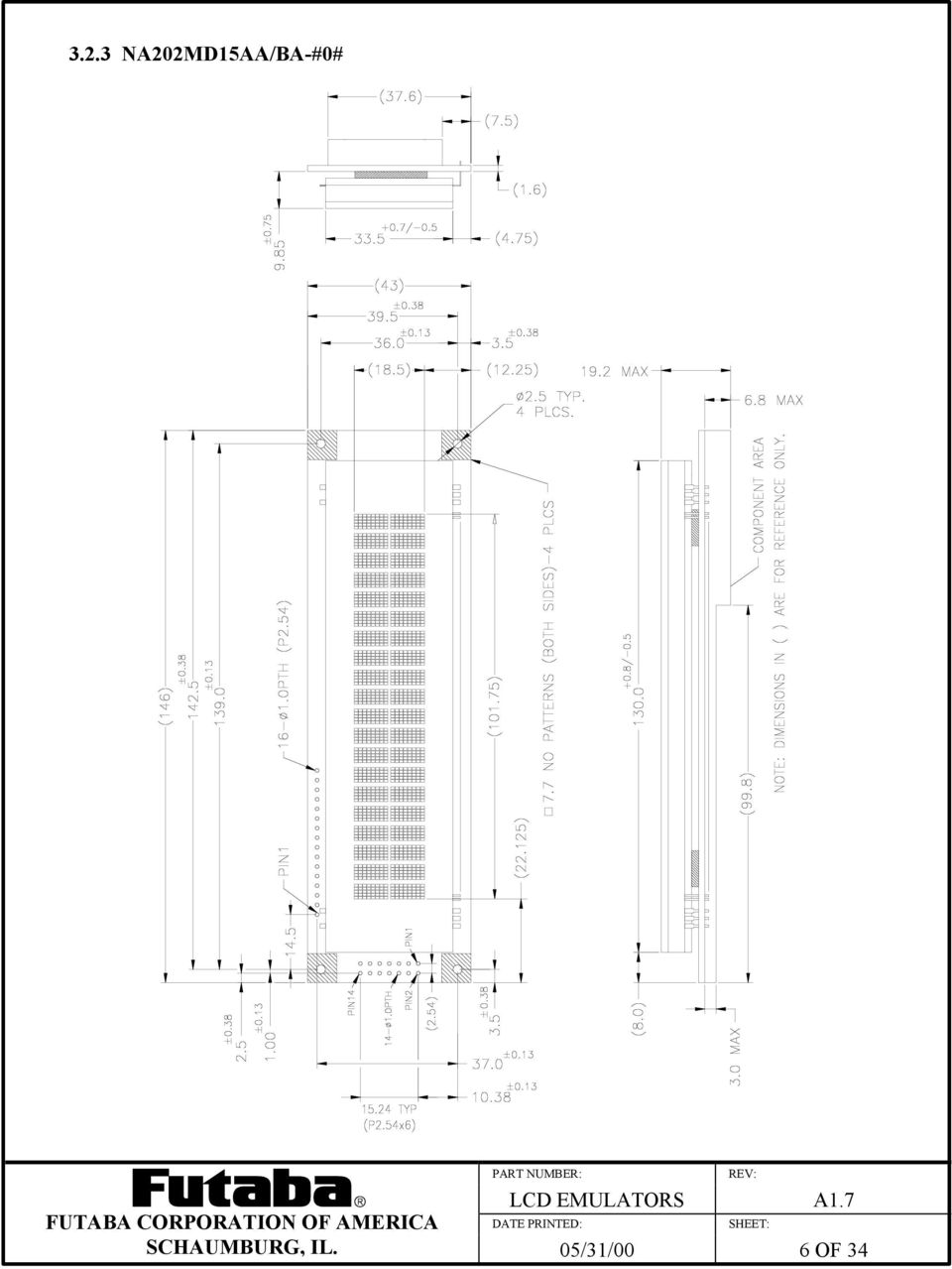
6 3.2.3 NA202MD15AA/BA-#0# 05/31/00 6 OF 34
7 3.2.4 NA202SD16AA/BA-#0# 05/31/00 7 OF 34

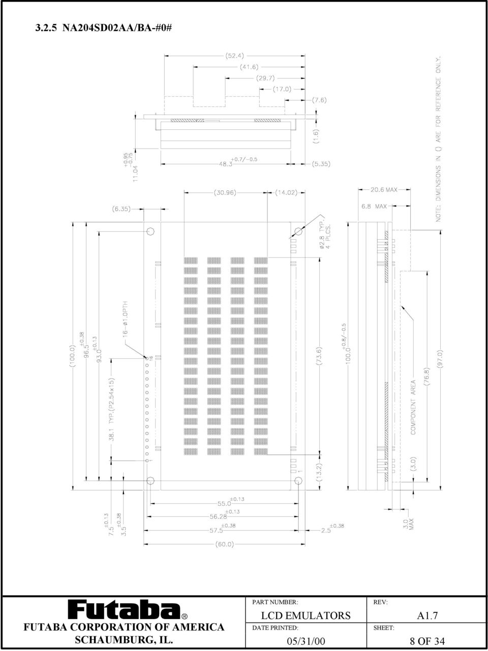
8 3.2.5 NA204SD02AA/BA-#0# 05/31/00 8 OF 34
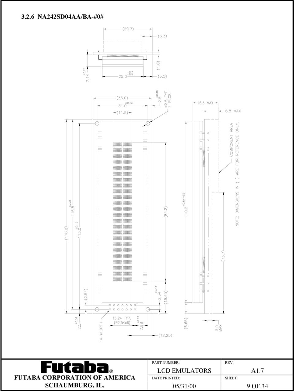
9 3.2.6 NA242SD04AA/BA-#0# 05/31/00 9 OF 34
10 3.2.7 NA402SD04AA/BA-#0# 05/31/00 10 OF 34

11 3.3 SYSTEM BLOCK DIAG NC_RST/_SI/SO RS_STB R/W_WR/ E_RD/_SCK DB0-DB7 DOT MATRIX VFD CONTROLLER AND DRIVER GRID DRIVER (IF NEEDED) VACUUM FLUORESCENT DISPLAY (SEE SECTION 2.0) Vcc GND DC-DC/AC CONVERTER 3.4 ENVIRONMENTAL SPECIFICATIONS Item Symbol Min. Max. Unit Comment Operating temperature Topr o C Storage temperature Tstg o C Operating humidity Hopr %RH Without condensation Storage humidity Hstg %RH Without condensation Vibration G Total amplitude: 1.5mm Freq: Hz sine wave Sweep time: 1 min./cycle Duration: 2 hrs./axis (X,Y,Z) Shock G Duration: 11ms Waveform: half sine wave 3 times/axis (X,Y,Z,-X,-Y,-Z) 3.5 ABSOLUTE MAXIMUM SPECIFICATIONS Item Symbol Min. Max. Unit Supply voltage V CC V Input signal voltage V IN -0.3 V CC +0.3 V 05/31/00 11 OF 34

12 3.6 DC ELECTRICAL SPECIFICATIONS Item Symbol Min. Typ. Max. Unit Supply voltage V CC V NA16SD08AA/BA-### Supply current NA162SD07AA/BA-### NA202MD15AA/BA-### NA202SD16AA/BA-### NA204SD02AA/BA-### NA242SD04AA/BA-### NA402SD10AA/BA-### High-level input voltage (see Note) (E,R/W,RD/,SCK,RST/) V IH1 0.8*V CC - V CC V Low-level input voltage (see Note) (E,R/W,RD/,SCK,RST/) V IL *V CC V High-level input voltage (see Note) (all inputs except E,R/W,RD/,SCK,RST/) V IH2 0.7*V CC - V CC V Low-level input voltage (see Note) (all inputs except E,R/W,RD/,SCK,RST/) V IL *V CC V High-level output voltage (I OH = -0.1mA) V OH V CC V Low-level output voltage (I OL = 0.1mA) V OL V Input current (see Note) I I ua Note: A 10K ohm pull-up resistor is provided on each input for TTL compatibility. 3.7 AC ELECTRICAL SPECIFICATIONS RESET TIMING (See Figures 1 and 2) Item Symbol Min. Max. Unit V CC rise time t RVCC - 10 ms V CC off time t OFF 1 - ms Delay time after power-up reset t IRSTD us Delay time after external reset t ERSTD us RST/ pulse width low t RSTL ns Input signal fall time t f - 15 ns Input signal rise time t r - 15 ns Note: All timing is specified using 20% and 80% of V CC as the reference points. I CC ma 05/31/00 12 OF 34
 (all inputs except E,R/W,RD/,SCK,RST/) V IH2 0.7*V CC - V CC V Low-level input voltage (see Note) (all inputs except E,R/W,RD/,SCK,RST/) V IL2 0.0-0.")
13 trvcc Vcc 0.2V 4.5V toff tirstd RS, STB Figure 1. Power-up Internal Reset Timing tf tr RST/ trstl terstd RS, STB Figure 2. External Reset Timing MOTOROLA M68-TYPE PARALLEL INTERFACE TIMING (See Figures 3 and 4) Item Symbol Min. Max. Unit RS, R/W setup time t AS 20 - ns RS, R/W hold time t AH 10 - ns Input signal rise time t r - 15 ns Input signal fall time t f - 15 ns E pulse width high PW EH ns E pulse width low PW EL ns Write data setup time t DS 80 - ns Write data hold time t DH 10 - ns E cycle time t CYCE ns Read data delay time t DD ns Read data hold time t DHR 5 - ns Note: All timing is specified using 20% and 80% of V CC as the reference points. 05/31/00 13 OF 34

14 RS tas tah R/W tr PW EH tf E tds tdh PW EL DB0-DB7 tcyce Figure 3. Motorola M68-Type Parallel Interface Write Cycle Timing RS tas tah R/W tr PW EH tf E PW EL tdd tdhr DB0-DB7 tcyce Figure 4. Motorola M68-Type Parallel Interface Read Cycle Timing 05/31/00 14 OF 34

15 3.7.3 INTEL I80-TYPE PARALLEL INTERFACE TIMING (See Figures 5 and 6) Item Symbol Min. Max. Unit RS setup time t RSS 10 - ns RS hold time t RSH 10 - ns Input signal fall time t f - 15 ns Input signal rise time t r - 15 ns WR/ pulse width low t WRL 30 - ns WR/ pulse width high t WRH ns Write data setup time t DSi 30 - ns Write data hold time t DHi 10 - ns WR/ cycle time t CYCWR ns RD/ cycle time t CYCRD ns RD/ pulse width low t RDL 70 - ns RD/ pulse width high t RDH ns Read data delay time t DDi - 70 ns Read data hold time t DHRi 5 80 ns Note: All timing is specified using 20% and 80% of V CC as the reference points. RS trss tf tr trsh twrh WR/ twrl tdsi tdhi DB0-DB7 tcycwr Figure 5. Intel I80-Type Parallel Interface Write Cycle Timing 05/31/00 15 OF 34

16 RS trss tf tr trsh trdh RD/ trdl tddi tdhri DB0-DB7 tcycrd Figure 6. Intel I80-Type Parallel Interface Read Cycle Timing SYNCHRONOUS SERIAL INTERFACE TIMING (See Figures 7, 8 and 12) Item Symbol Min. Max. Unit STB setup time t STBS ns STB hold time t STBH ns Input signal fall time t f - 15 ns Input signal rise time t r - 15 ns STB pulse width high t WSTB ns SCK pulse width high t SCKH ns SCK pulse width low t SCKL ns SI data setup time t DSs ns SI data hold time t DHs ns SCK cycle time t CYCSCK ns SCK wait time between bytes t WAIT 1 - us SO data delay time t DDs ns SO data hold time t DHRs 5 - ns Note: All timing is specified using 20% and 80% of V CC as the reference points. 05/31/00 16 OF 34

17 twstb STB tstbs tcycsck tsckh tstbh SCK tf tsckl tdss tdhs tr SI/SO Figure 7. Synchronous Serial Interface Write Cycle Timing twstb STB tstbs tcycsck tsckh tstbh SCK tf tsckl tdhrs tr tdds SI/SO Figure 8. Synchronous Serial Interface Read Cycle Timing 05/31/00 17 OF 34

18 4.0 MODES OF OPERATION The following modes of operation are selectable via jumpers (see section 8.0 Jumper Settings). 4.1 PARALLEL INTERFACE MODES In the parallel interface mode, 8-bit instructions and data are sent between the host and the modules using either 4-bit nibbles or 8-bit bytes. Nibbles are transmitted high nibble first on DB4-DB7 (DB0-DB3 are ignored) whereas bytes are transmitted on DB0-DB7. The Register Select (RS) control signal is used to identify DB0-DB7 as an instruction (low) or data (high) MOTOROLA M68-TYPE MODE This mode uses the Read/Write (R/W) and Enable (E) control signals to transfer information. Instructions/data are written to the modules on the falling edge of E when R/W is low and are read from the modules after the rising edge of E when R/W is high. RS R/W E DB7 IB7 IB3 IB7 IB3 BF= '0' IB3 DB7 DB3 DB6 IB6 IB2 IB6 IB2 IB6 IB2 DB6 DB2 DB5 IB5 IB1 IB5 IB1 IB5 IB1 DB5 DB1 DB4 IB4 IB0 IB4 IB0 IB4 IB0 DB4 DB0 Write instruction Write instruction Read instruction Write data Figure 9. Typical 4-Bit Parallel Interface Sequence Using M68-Type Mode 05/31/00 18 OF 34
 control signal is used to identify DB0-DB7 as an instruction (low) or data (high). 4.1.")
19 4.1.2 INTEL I80-TYPE MODE This mode uses the Read (RD/) and Write (WR/) control signals to transfer information. Instructions/data are written to the modules on the rising edge of WR/ and are read from the modules after the falling edge of RD/. RS WR/ RD/ DB7 IB7 IB7 BF= '0' DB7 DB6 IB6 IB6 IB6 DB6 DB0 IB0 IB0 IB0 DB0 Write instruction Write instruction Read instruction Write data Figure 10. Typical 8-Bit Parallel Interface Sequence Using I80-Type Mode 4.2 SYNCHRONOUS SERIAL INTERFACE MODE In the synchronous serial interface mode, instructions and data are sent between the host and the modules using 8-bit bytes. Two bytes are required per read/write cycle and are transmitted MSB first. The start byte contains 5 high bits, the Read/Write (R/W) control bit, the Register Select (RS) control bit, and a low bit. The following byte contains the instruction/data bits. The R/W bit determines whether the cycle is a read (high) or a write (low) cycle. The RS bit is used to identify the second byte as an instruction (low) or data (high). This mode uses the Strobe (STB) control signal, Serial Clock (SCK) input, and Serial I/O (SI/SO) line to transfer information. In a write cycle, bits are clocked into the modules on the rising edge of SCK. In a read cycle, bits in the start byte are clocked into the modules on the rising edge of SCK. After the minimum wait time, each bit in the instruction/data byte can be read from the modules after each falling edge of SCK. Each read/write cycle begins on the falling edge of STB and ends on the rising edge. To be a valid read/write cycle, the STB must go high at the end of the cycle. 05/31/00 19 OF 34

20 STB SCK SI/SO '1' '1' '1' '1' '1' R/W RS '0' B7 B6 B5 B4 B3 B2 B1 B0 Start byte Instruction / Data Figure 11. Typical Synchronous Serial Interface Write Cycle STB SCK twait SI/SO '1' '1' '1' '1' '1' R/W RS '0' B7 B6 B5 B4 B3 B2 B1 B0 Start byte Instruction / Data Figure 12. Typical Synchronous Serial Interface Read Cycle 4.3 RESET MODES The modules are reset automatically at power-up by an internal R-C circuit. However, an external reset mode can also be selected when using one of the parallel interface modes (this option is not available when using the synchronous serial interface mode). This mode allows the modules to be reset by setting the Reset (RST/) input low. 05/31/00 20 OF 34
.")
21 5.0 CHARACTER FONT TABLES 5.1 ENGLISH / KATAKANA CHARACTER FONT (Option A) UPPER NIBBLE LOWER NIBBLE (1) 0001 (2) 0010 (3) 0011 (4) 0100 (5) 0101 (6) 0110 (7) 0111 (8) 1000 (1) 1001 (2) 1010 (3) 1011 (4) 1100 (5) 1101 (6) 1110 (7) 1111 (8) 05/31/00 21 OF 34
22 5.2 ENGLISH / EUROPEAN CHARACTER FONT (Option B) UPPER NIBBLE LOWER NIBBLE (1) 0001 (2) 0010 (3) 0011 (4) 0100 (5) 0101 (6) 0110 (7) 0111 (8) 1000 (1) 1001 (2) 1010 (3) 1011 (4) 1100 (5) 1101 (6) 1110 (7) 1111 (8) 05/31/00 22 OF 34
23 6.0 FUNCTIONAL DESCRIPTION 6.1 ADDRESS COUNTER (AC) SINGLE LINE DISPLAYS The AC stores the address of the data being written to and read from DD or. The AC increments by 1 (overflows from 4FH to 00H) or decrements by 1 (underflows from 00H to 4FH) after each DD access. The AC increments by 1 (overflows from 3FH to 00H) or decrements by 1 (underflows from 00H to 3FH) after each access. When addressing DD, the value in the AC also represents the cursor position MULTIPLE LINE DISPLAYS The AC stores the address of the data being written to and read from DD or. The AC increments by 1 (overflows from 27H to 40H and from 67H to 00H) or decrements by 1 (underflows from 40H to 27H and from 00H to 67H) after each DD access. The AC increments by 1 (overflows from 3FH to 00H) or decrements by 1 (underflows from 00H to 3FH) after each access. When addressing DD, the value in the AC also represents the cursor position. 6.2 DISPLAY DATA (DD) SINGLE LINE DISPLAYS The DD stores the character code of each character being displayed on the VFD. Valid DD addresses are 00H to 4FH. DD not being used for display characters can be used as general purpose. The tables below show the relationship between the DD address and the character position on the VFD before and after a display shift (with the number of display lines set to 1) MULTIPLE LINE DISPLAYS The DD stores the character code of each character being displayed on the VFD. Valid DD addresses are 00H to 27H and 40H to 67H. DD not being used for display characters can be used as general purpose. The tables below show the relationship between the DD address and the character position on the VFD before and after a display shift (with the number of display lines set to 2). 05/31/00 23 OF 34
24 6.3 DISPLAY SHIFT DETAIL NA16SD08AA/BA-### Relationship before a display shift (non-shifted): A 0B 0C 0D 0E 0F Relationship after a display shift to the left: A 0B 0C 0D 0E 0F 10 Relationship after a display shift to the right: F A 0B 0C 0D 0E NA162SD08AA/BA-### Relationship before a display shift (non-shifted): A 0B 0C 0D 0E 0F A 4B 4C 4D 4E 4F Relationship after a display shift to the left: A 0B 0C 0D 0E 0F A 4B 4C 4D 4E 4F 50 Relationship after a display shift to the right: A 0B 0C 0D 0E A 4B 4C 4D 4E 05/31/00 24 OF 34
25 6.3.3 NA202MD15AA/BA-### AND NA202SD16AA/BA-### Relationship before a display shift (non-shifted): A 0B 0C 0D 0E 0F A 4B 4C 4D 4E 4F Relationship after a display shift to the left: A 0B 0C 0D 0E 0F A 4B 4C 4D 4E 4F Relationship after a display shift to the right: A 0B 0C 0D 0E 0F A 4B 4C 4D 4E 4F NA204SD02AA/BA-### Relationship before a display shift (non-shifted): A 0B 0C 0D 0E 0F A 4B 4C 4D 4E 4F A 1B 1C 1D 1E 1F A 5B 5C 5D 5E 5F Relationship after a display shift to the left: A 0B 0C 0D 0E 0F A 4B 4C 4D 4E 4F A 1B 1C 1D 1E 1F A 5B 5C 5D 5E 5F Relationship after a display shift to the right: A 0B 0C 0D 0E 0F A 4B 4C 4D 4E 4F A 1B 1C 1D 1E 1F A 5B 5C 5D 5E 5F /31/00 25 OF 34
26 6.3.5 NA242SD04AA/BA-### Relationship before a display shift (non-shifted): A 0B 0C 0D 0E 0F A 4B 4C 4D 4E 4F Relationship after a display shift to the left: A 0B 0C 0D 0E 0F A 4B 4C 4D 4E 4F Relationship after a display shift to the right: A 0B 0C 0D 0E 0F A 4B 4C 4D 4E 4F NA402SD10AA/BA-### Relationship before a display shift (non-shifted): F F Relationship after a display shift to the left: Relationship after a display shift to the right: E 1F E 5F /31/00 26 OF 34
27 6.4 CHARACTER GENERATOR () The stores the pixel information (1 = pixel on, 0 = pixel off) for the eight userdefinable 5x8 characters. Valid addresses are 00H to 3FH. not being used to define characters can be used as general purpose (lower 5 bits only). Character codes 00H to 07H (or 08H to 0FH) are assigned to the user-definable characters (see section 5.0 Character Font Tables). The table below shows the relationship between the character codes, addresses, and data for each user-definable character. Character code address data D7 D6 D5 D4 D3 D2 D1 D0 A5 A4 A3 A2 A1 A0 D7 D6 D5 D4 D3 D2 D1 D X X X X X X X X (1) (2) X x = don't care X X X (8) 6.5 INSTRUCTIONS Instruction RS R/W DB7 DB6 DB5 DB4 DB3 DB2 DB1 DB0 Clear display Cursor home x Entry mode set I/D S Display on/off control D C B Cursor/display shift S/C R/L x x Function set DL N x BR1 BR0 address set address DD address set DD address Address counter read 0 1 BF=0 AC contents DD or write 1 0 Write data DD or read 1 1 Read data x = don t care 05/31/00 27 OF 34
28 6.5.1 CLEAR DISPLAY RS R/W DB7 DB6 DB5 DB4 DB3 DB2 DB1 DB This instruction clears the display (without affecting the contents of ) by performing the following: 1) Fills all DD locations with character code 20H (character code for a space). 2) Sets the AC to DD address 00H (i.e. sets cursor position to 00H). 3) Returns the display to the non-shifted position. 4) Sets the I/D bit to CURSOR HOME RS R/W DB7 DB6 DB5 DB4 DB3 DB2 DB1 DB x x = don t care This instruction returns the cursor to the home position (without affecting the contents of DD or ) by performing the following: 1) Sets the AC to DD address 00H (i.e. sets cursor position to 00H). 2) Returns the display to the non-shifted position ENTRY MODE SET RS R/W DB7 DB6 DB5 DB4 DB3 DB2 DB1 DB I/D S This instruction selects whether the AC (cursor position) increments or decrements after each DD or access and determines the direction the information on the display shifts after each DD write. The instruction also enables or disables display shifts after each DD write (information on the display does not shift after a DD read or access). DD,, and AC contents are not affected by this instruction. I/D = 0: The AC decrements after each DD or access. If S = 1, the information on the display shifts to the right by one character position after each DD write. I/D = 1: The AC increments after each DD or access. If S = 1, the information on the display shifts to the left by one character position after each DD write. S = 0: S = 1: The display shift function is disabled. The display shift function is enabled. 05/31/00 28 OF 34
29 6.5.4 DISPLAY ON/OFF CONTROL RS R/W DB7 DB6 DB5 DB4 DB3 DB2 DB1 DB D C B This instruction selects whether the display and cursor are on or off and selects whether or not the character at the current cursor position blinks. DD,, and AC contents are not affected by this instruction. D = 0: D = 1: C = 0: C = 1: B = 0: B = 1: The display is off (display blank). The display is on (contents of DD displayed). The cursor is off. The cursor is on (8 th row of pixels). The blinking character function is disabled. The blinking character function is enabled (a character with all pixels on will alternate with the character displayed at the current cursor position at about a 1Hz rate with a 50% duty cycle) CURSOR/DISPLAY SHIFT RS R/W DB7 DB6 DB5 DB4 DB3 DB2 DB1 DB S/C R/L x x x = don t care This instruction increments or decrements the AC (cursor position) and shifts the information on the display one character position to the left or right without accessing DD or. DD and contents are not affected by this instruction. If the AC was addressing prior to this instruction, the AC will be addressing DD after this instruction. However, if the AC was addressing DD prior to this instruction, the AC will still be addressing DD after this instruction. S/C R/L AC contents (cursor position) Information on the display 0 0 Decrements by one No change 0 1 Increments by one No change 1 0 Decrements by one Shifts one character position to the left 1 1 Increments by one Shifts one character position to the right 05/31/00 29 OF 34
30 6.5.6 FUNCTION SET RS R/W DB7 DB6 DB5 DB4 DB3 DB2 DB1 DB DL N x BR1 BR0 x = don t care This instruction sets the width of the data bus for the parallel interface modes, the number of display lines, and the luminance level (brightness) of the VFD. It must be the first command sent after any reset. DD,, and AC contents are not affected by this instruction. DL = 0: Sets the data bus width for the parallel interface modes to 4-bit (DB7-DB4). DL = 1: Sets the data bus width for the parallel interface modes to 8-bit (DB7-DB0). N = 0: N = 1: Sets the number of display lines to 1 (this setting is not recommended for multiple line displays). Sets the number of display lines to 2 (this setting is not recommended for single line displays). BR1,BR0 = 0,0: Sets the luminance level to 100%. 0,1: Sets the luminance level to 75%. 1,0: Sets the luminance level to 50%. 1,1: Sets the luminance level to 25% ADDRESS SET RS R/W DB7 DB6 DB5 DB4 DB3 DB2 DB1 DB address This instruction places the 6-bit address specified by DB5-DB0 into the AC (cursor position). Subsequent data writes (reads) will be to (from). DD and contents are not affected by this instruction DD ADDRESS SET RS R/W DB7 DB6 DB5 DB4 DB3 DB2 DB1 DB DD address This instruction places the 7-bit DD address specified by DB6-DB0 into the AC (cursor position). Subsequent data writes (reads) will be to (from) DD. DD and contents are not affected by this instruction. 05/31/00 30 OF 34
31 6.5.9 ADDRESS COUNTER READ RS R/W DB7 DB6 DB5 DB4 DB3 DB2 DB1 DB0 0 1 BF=0 AC contents This instruction reads the current 7-bit address from the AC on DB6-DB0 and the busy flag (BF) bit (always 0) on DB7. DD,, and AC contents are not affected by this instruction. Because the BF is always 0, the host never has to read the BF bit to determine if the modules are busy before sending data or instructions. Therefore, data and instructions can be sent to the modules continuously according to the E, WR/, and SCK cycle times specified in section 3.7 AC Timing Specifications. Due to this feature, the execution times for each instruction are not specified DD OR WRITE RS R/W DB7 DB6 DB5 DB4 DB3 DB2 DB1 DB0 1 0 Write data This instruction writes the 8-bit data byte on DB7-DB0 into the DD or location addressed by the AC. The most recent DD or Address Set instruction determines whether the write is to DD or. This instruction also increments or decrements the AC and shifts the display according to the I/D and S bits set by the Entry Mode Set instruction DD OR READ RS R/W DB7 DB6 DB5 DB4 DB3 DB2 DB1 DB0 1 1 Read data This instruction reads the 8-bit data byte from the DD or location addressed by the AC on DB7-DB0. The most recent DD or Address Set instruction determines whether the read is from DD or. This instruction also increments or decrements the AC and shifts the display according to the I/D and S bits set by the Entry Mode Set instruction. Before sending this instruction, a DD or Address Set instruction should be executed to set the AC to the desired DD or address to be read. 05/31/00 31 OF 34
32 6.6 RESET CONDITIONS After either a power-up reset or an external reset, the modules initialize to the following conditions: 1) All DD locations are set to 20H (character code for a space). 2) The AC is set to DD address 00H (i.e. sets cursor position to 00H). 3) The relationship between DD addresses and character positions on the VFD is set to the non-shifted position. 4) Entry Mode Set instruction bits: I/D = 1: The AC increments after each DD or access. S = 0: The display shift function is disabled. 5) Display On/Off Control instruction bits: D = 0: The display is off (display blank). C = 0: The cursor is off. B = 0: The blinking character function is disabled. 6) Function Set instruction bits: DL = 1: Sets the data bus width for the parallel interface modes to 8-bit (DB7-DB0). N = 1(0): Number of display lines set to 2 for multiple line displays (number of display lines set to 1 for single line displays). BR1,BR0 = 0,0: Sets the luminance level to 100%. Note that the function set command must be the first instruction sent to the module after any reset INITIALIZATION The modules can be initialized by using instructions if the modules are not reset according to the reset timing detailed in Section (Reset Timing). After any reset, the function set command must be the first instruction sent to the module. 05/31/00 32 OF 34
33 7.0 CONNECTOR INTERFACE Pin No. Serial Parallel (Intel) Parallel (Motorola) Pin No. Serial Parallel (Intel) Parallel (Motorola) 1 GND GND GND 2 V CC V CC V CC 3 SI/SO NC or RST/ NC or RST/ 4 STB RS RS 5 NC WR/ R/W 6 SCK RD/ E 7 NC DB0 DB0 8 NC DB1 DB1 9 NC DB2 DB2 10 NC DB3 DB3 11 NC DB4 DB4 12 NC DB5 DB5 13 NC DB6 DB6 14 NC DB7 DB7 15* NC NC NC 16* NC NC NC NC = No Connection *If applicable. 7.1 CONNECTOR CONFIGURATION Product Number Connector (if applicable) Configuration NA16SD08AA/BA-#1# Amp P/N or equivalent 1 x 15 NA162SD07AA/BA-#1# Amp P/N or equivalent 1 x 14 NA202MD15AA/BA-#1#* Berg P/N or equivalent 2 x 7 NA202SD16AA/BA-#1# Berg P/N or equivalent 2 x 7 NA204SD02AA/BA-#1# Amp P/N or equivalent 1 x 16 NA242SD04AA/BA-#1# Berg P/N or equivalent 2 x 7 NA402SD10AA/BA-#1# Berg P/N or equivalent 2 x 7 *Also has holes that accept a 1 x 16 connector, Amp P/N or equivalent. 05/31/00 33 OF 34
34 8.0 JUMPER SETTINGS Mode JP2 JP3 JP4 JP5 JP6 JP7 Parallel (Motorola) (Note 1) open shorted open shorted open Parallel (Intel) (Note 1) open shorted open open shorted Serial open shorted open shorted shorted open Note 1: JP2 shorted (open) enables (disables) external reset mode. 9.0 PART NUMBER OPTIONS NA202SD16BA : Internal R-C reset 1: External reset 0: Without connector 1: With straight pin header connector mounted on component side #: Customer specified connector - Contact Futaba for this option 0: Motorola M68-type parallel interface 1: Intel I80-type parallel interface 2: Serial type interface Sequential revision letter (see revision tables for current letter) A: English - Katakana character font B: English - European character font This example defines a 20 x 2 LCD Emulator display with English - European character font, revision letter A, Motorola M68-type interface, no connector, and external reset. 05/31/00 34 OF 34
SPECIFICATION NO. : DS-1601-0000-00. D A T E O F I S S U E : July 16, 2010. R E V I S I O N : September 1, 2010 (00) : : :
 : : :") RoHS 22/95/EC VACUUM FLUORESCENT DISPLAY MODULE SPECIFICATION MODEL: CU229-UWJ SPECIFICATION NO. : DS-6-- D A T E O F I S S U E : July 6, 2 (R) R E V I S I O N : September, 2 () : : : PUBLISHED BY NORITAKE
RoHS 22/95/EC VACUUM FLUORESCENT DISPLAY MODULE SPECIFICATION MODEL: CU229-UWJ SPECIFICATION NO. : DS-6-- D A T E O F I S S U E : July 6, 2 (R) R E V I S I O N : September, 2 () : : : PUBLISHED BY NORITAKE
VACUUM FLUORESCENT DISPLAY MODULE SPECIFICATION. Model: CU16025ECPB-W6J
 VACUUM FLUORESCENT DISPLAY MODULE SPECIFICATION Model: CU16025ECPB-W6J SPECIFICATION NO.: DS-947-0000-00 DATE OF ISSUE : Aug. 2, 2000 REVISION : Nov. 6, 2002 PUBLISHED BY : NORITAKE ITRON Corp. / JAPAN
LMB162ABC LCD Module User Manual
 LMB162ABC LCD Module User Manual Shenzhen TOPWAY Technology Co., Ltd. Rev. Descriptions Release Date 0.1 Prelimiay release 2005-03-17 0.2 Typing Correction in 1.3 Block Diagram 2007-05-06 URL Document
GDM1602A SPECIFICATIONS OF LCD MODULE. Features. Outline dimension
 SPECIFICATIONS OF LCD MODULE Features 1. 5x8 dots 2. Built-in controller (S6A0069 or Equivalent) 3. Power supply: Type 5V 4. 1/16 duty cycle 5. LED backlight 6. N.V. option Outline dimension Absolute maximum
HD44780-Based LCD Modules. Introduction to the LM018L
 HD44780-Based LCD Modules Hitachi LM018L 40 character x 2 lines Built-in LSI HD44780 controller +5volt single power supply Display Colour: Grey LM018L: Introduction Interfacing Display Pattern and Character
BATRON DOCUMENT NUMBER AND REVISION VL-FS-BTHQ 21605VSS-02 REV.A (BTHQ 21605VSS-FSTF-LED05W(1 DIE)) Feb/2002 BTHQ 21605-FSTF-LED WHITE 1/15
) Feb/2002 BTHQ 21605-FSTF-LED WHITE 1/15") Feb/2002 1/15 DOCUMENT NUMBER AND REVISION VL-FS-BTHQ 21605VSS-02 REV.A (BTHQ 21605VSS-FSTF-LED05W(1 DIE)) 2/15 DOCUMENT REVISION HISTORY 1: DOCUMENT REVISION DATE DESCRIPTION CHANGED BY FROM TO A 2002.01.09
Feb/2002 1/15 DOCUMENT NUMBER AND REVISION VL-FS-BTHQ 21605VSS-02 REV.A (BTHQ 21605VSS-FSTF-LED05W(1 DIE)) 2/15 DOCUMENT REVISION HISTORY 1: DOCUMENT REVISION DATE DESCRIPTION CHANGED BY FROM TO A 2002.01.09
LCM Design Engineering SPECIFICATION FOR LCD MODULE TYPE ITEM NO.: MDLS16265-04 MDLS16265-LV-G-LED04G (BB) (DOC. REVISION 1.0)
 (DOC. REVISION 1.0)") VARITRONIX LIMITED LCM Design Engineering SPECIFICATION FOR LCD MODULE TYPE ITEM NO.: MDLS16265-04 MDLS16265-LV-G-LED04G (BB) (DOC. REVISION 1.0) DEPARTMENT NAME SIGNATURE EFFECTIVE DATE PREPARED BY PHILIP
VARITRONIX LIMITED LCM Design Engineering SPECIFICATION FOR LCD MODULE TYPE ITEM NO.: MDLS16265-04 MDLS16265-LV-G-LED04G (BB) (DOC. REVISION 1.0) DEPARTMENT NAME SIGNATURE EFFECTIVE DATE PREPARED BY PHILIP
LCD MODULE DEM 16481 SYH-LY
 DISPLAY Elektronik GmbH LCD MODULE DEM 16481 SYH-LY Version :1.1.1 16/Jan/2009 GENERAL SPECIFICATION MODULE NO. : DEM 16481 SYH-LY CUSTOMER P/N VERSION NO. CHANGE DESCRIPTION DATE 0 ORIGINAL VERSION 16.01.2001
LCM NHD-12032BZ-FSW-GBW. User s Guide. (Liquid Crystal Display Graphic Module) RoHS Compliant. For product support, contact
 RoHS Compliant. For product support, contact") User s Guide -FSW-GBW LCM (Liquid Crystal Display Graphic Module) RoHS Compliant NHD- 12032- BZ- F - SW- G- B- W- Newhaven Display 120 x 32 pixels Version Line Transflective Side White LED B/L STN- Gray
User s Guide -FSW-GBW LCM (Liquid Crystal Display Graphic Module) RoHS Compliant NHD- 12032- BZ- F - SW- G- B- W- Newhaven Display 120 x 32 pixels Version Line Transflective Side White LED B/L STN- Gray
LCD MODULE DEM 16217 SYH-LY
 Display Elektronik GmbH LCD MODULE DEM 16217 SYH-LY Product specification Version : 5 14.04.2003 GENERAL SPECIFICATION MODULE NO. : DEM 16217 SYH-LY CUSTOMER P/N VERSION NO. CHANGE DESCRIPTION DATE 0 ORIGINAL
EMERGING DISPLAY CUSTOMER ACCEPTANCE SPECIFICATIONS 16400(LED TYPES) EXAMINED BY : FILE NO. CAS-10068 ISSUE : JAN.19,2000 TOTAL PAGE : 7 APPROVED BY:
 EXAMINED BY : FILE NO. CAS-10068 ISSUE : JAN.19,2000 TOTAL PAGE : 7 APPROVED BY:") EXAMINED BY : FILE NO. CAS-10068 APPROVED BY: EMERGING DISPLAY TECHNOLOGIES CORPORATION ISSUE : JAN.19,2000 TOTAL PAGE : 7 VERSION : 3 CUSTOMER ACCEPTANCE SPECIFICATIONS MODEL NO. : 16400(LED TYPES) FOR
EXAMINED BY : FILE NO. CAS-10068 APPROVED BY: EMERGING DISPLAY TECHNOLOGIES CORPORATION ISSUE : JAN.19,2000 TOTAL PAGE : 7 VERSION : 3 CUSTOMER ACCEPTANCE SPECIFICATIONS MODEL NO. : 16400(LED TYPES) FOR
EMERGING DISPLAY CUSTOMER ACCEPTANCE SPECIFICATIONS 20400 (LED TYPES) EXAMINED BY : FILE NO. CAS-10184 ISSUE : DEC.01,1999 TOTAL PAGE : 7 APPROVED BY:
 EXAMINED BY : FILE NO. CAS-10184 ISSUE : DEC.01,1999 TOTAL PAGE : 7 APPROVED BY:") EXAMINED BY : FILE NO. CAS-10184 APPROVED BY: EMERGING DISPLAY TECHNOLOGIES CORPORATION ISSUE : DEC.01,1999 TOTAL PAGE : 7 VERSION : 2 CUSTOMER ACCEPTANCE SPECIFICATIONS MODEL NO. : 20400 (LED TYPES) FOR
EXAMINED BY : FILE NO. CAS-10184 APPROVED BY: EMERGING DISPLAY TECHNOLOGIES CORPORATION ISSUE : DEC.01,1999 TOTAL PAGE : 7 VERSION : 2 CUSTOMER ACCEPTANCE SPECIFICATIONS MODEL NO. : 20400 (LED TYPES) FOR
EMERGING DISPLAY CUSTOMER ACCEPTANCE SPECIFICATIONS 16290(LED TYPES) EXAMINED BY : FILE NO. CAS-10251 ISSUE : JUL.03,2001 TOTAL PAGE : 7
 EXAMINED BY : FILE NO. CAS-10251 ISSUE : JUL.03,2001 TOTAL PAGE : 7") EXAMINED BY : FILE NO. CAS-10251 EMERGING DISPLAY ISSUE : JUL.03,2001 APPROVED BY: TECHNOLOGIES CORPORATION TOTAL PAGE : 7 VERSION : 1 CUSTOMER ACCEPTANCE SPECIFICATIONS MODEL NO. : 16290(LED TYPES) FOR
EXAMINED BY : FILE NO. CAS-10251 EMERGING DISPLAY ISSUE : JUL.03,2001 APPROVED BY: TECHNOLOGIES CORPORATION TOTAL PAGE : 7 VERSION : 1 CUSTOMER ACCEPTANCE SPECIFICATIONS MODEL NO. : 16290(LED TYPES) FOR
OPTREX CORP. LCD MODULE
 MITSUBISHI INTERNATIONAL GMBH OPTREX CORP. LCD MODULE ALPHANUMERIC TYPE DMC SERIES USER S MANUAL FOR LCD MODULE WITH CONTROLLER HITACHI HD44780 Mitsubishi International GmbH Kennedydamm 19 D-40476 Düsseldorf
LCD Module User Manual
 LCD Module User Manual Customer : Ordering Code DRAWING NO : TC1602D-02WB0 : m-tc1602d-02wb0_a00 Approved By Customer: Date: Approved By Checked By Prepared By LET (HK) PACIFIC CO, LTD ADD:Flat B1,5/F,Yip
DOT MATRIX CHARACTER LCD MODULE USER S MANUAL
 DOT MATRIX CHARACTER LCD MODULE USER S MANUAL OPTREX CORPORATION 1 Revision # Description Date Revised 2 Preface This user s manual has been prepared for all users of the OPTREX DMC series Liquid Crystal
SPECIFICATIONS FOR LIQUID CRYSTAL DISPLAY
 SPECIFICATIONS FOR LIQUID CRYSTAL DISPLAY PART NUMBER: MGD1602B DATE: MAR. 17,2004 1.0 MECHANICAL SPECS 1. Overall Module Size 84.0mm(W) x 44.0mm(H) x max 13.5mm(D) for LED backlight version 84.0mm(W)
HD44780U (LCD-II) (Dot Matrix Liquid Crystal Display Controller/Driver)
 (Dot Matrix Liquid Crystal Display Controller/Driver)") HD4478U (LCD-II) (Dot Matrix Liquid Crystal Display Controller/Driver) Description The HD4478U dot-matrix liquid crystal display controller and driver LSI displays alphanumerics, Japanese kana characters,
HD4478U (LCD-II) (Dot Matrix Liquid Crystal Display Controller/Driver) Description The HD4478U dot-matrix liquid crystal display controller and driver LSI displays alphanumerics, Japanese kana characters,
NHD-0420D3Z-FL-GBW-V3
 NHD-0420D3Z-FL-GBW-V3 Serial Liquid Crystal Display Module NHD- Newhaven Display 0420-4 Lines x 20 Characters D3Z- Model F- Transflective L- Yellow/Green LED Backlight G- STN-Gray B- 6:00 Optimal View
Specification. For. LCD Module CCM1620CSL
 Specification For LCD Module CCM1620CSL 1 FEATURES CASIL SEMICONDUCTOR CO., LTD. CCM1620CSL LCD MODULE Display Type: STN Display Format: 16 Characters x 2 Lines Input Data: 4-Bits or 8-Bits interface available
HD44780U (LCD-II) A single HD44780U can display up to one 8-character line or two 8-character lines.
 A single HD44780U can display up to one 8-character line or two 8-character lines.") HD4478U (LCD-II) (Dot Matrix Liquid Crystal Display Controller/Driver) ADE-27-272(Z) '99.9 Rev.. Description The HD4478U dot-matrix liquid crystal display controller and driver LSI displays alphanumerics,
HD4478U (LCD-II) (Dot Matrix Liquid Crystal Display Controller/Driver) ADE-27-272(Z) '99.9 Rev.. Description The HD4478U dot-matrix liquid crystal display controller and driver LSI displays alphanumerics,
MGL5128 128x64 Graphic LCD Module User Manual
 MGL5128 128x64 Graphic LCD Module User Manual Version: 1.0.0 January 2005 Table of Contents I Precautions in use of LCD Modules 2 II General Specification 2 III Absolute Maximum Ratings 2 IV Electrical
SPECIFICATIONS FOR LCD MODULE
 A M P I R E SPECIFICATIONS FOR LCD MODULE CUSTOMER CUSTOMER PART NO. AMPIRE PART NO. -162B APPROVED BY DATE APPROVED BY CHECKED BY ORGANIZED BY AMPIRE CO., LTD. 1 RECORD OF REVISION Revision Date Page
LCD MODULE DEM 128064B FGH-PW
 DISPLAY Elektronik GmbH LCD MODULE DEM 128064B FGHPW Version : 2.1.1 30.09.2008 GENERAL SPECIFICATION MODULE NO. : DEM 128064B FGHPW VERSION NO. CHANGE DESCRIPTION DATE 0 ORIGINAL VERSION 27.11.2006 1
LCD MODULE SPECIFICATION MODEL NO. BG12864EFPHHn
 LCD MODULE SPECIFICATION MODEL NO. BG12864EFPHHn FOR MESSRS: ON DATE OF: APPROVED BY: C O N T E N T S 1. Numbering System 2. General Specification 3. Absolute Maximum Ratings 4. Electrical Characteristics
PACKAGE OUTLINE DALLAS DS2434 DS2434 GND. PR 35 PACKAGE See Mech. Drawings Section
 PRELIMINARY DS2434 Battery Identification Chip FEATURES Provides unique ID number to battery packs PACKAGE OUTLINE Eliminates thermistors by sensing battery temperature on chip DALLAS DS2434 1 2 3 256
HD61202U. (Dot Matrix Liquid Crystal GraphicDisplay Column Driver)
") HD622U (Dot Matrix Liquid Crystal GraphicDisplay Column Driver) Description HD622U is a column (segment) driver for dot matrix liquid crystal graphic display systems. It stores the display data transferred
HD622U (Dot Matrix Liquid Crystal GraphicDisplay Column Driver) Description HD622U is a column (segment) driver for dot matrix liquid crystal graphic display systems. It stores the display data transferred
NT7606. STN LCDController/Driver. RAM-Map STN LCD Controller/Driver. Preliminary
 16C Characters X 3L Character X 3 Lines + 80 + icon 80 icons RAM-Map STN LCD Controller/Driver STN LCDController/Driver V0.04 V1.0 Preliminary Revision History...3 Features...4 General Description...4
KS0108B 64CH SEGMENT DRIVER FOR DOT MATRIX LCD INTRODUCTION 100 QFP
 INTRODUCTION 100 QFP The KS0108B is a LCD driver LSl with 64 channel output for dot matrix liquid crystal graphic display system. This device consists of the display RAM, 64 bit data latch 64 bit drivers
SPECIFICATION CUSTOMER : APPROVED BY: ( FOR CUSTOMER USE ONLY ) SALES BY APPROVED BY CHECKED BY PREPARED BY ISSUED DATE:
 SALES BY APPROVED BY CHECKED BY PREPARED BY ISSUED DATE:") SPECIFICATION CUSTOMER : MODULE NO.: PH216B-BYB-E APPROVED BY: ( FOR CUSTOMER USE ONLY ) SALES BY APPROVED BY CHECKED BY PREPARED BY ISSUED DATE: Contents 1.Module Classification Information 2.Precautions
SPECIFICATION CUSTOMER : MODULE NO.: PH216B-BYB-E APPROVED BY: ( FOR CUSTOMER USE ONLY ) SALES BY APPROVED BY CHECKED BY PREPARED BY ISSUED DATE: Contents 1.Module Classification Information 2.Precautions
8 by 8 dot matrix LED displays with Cascadable Serial driver B32CDM8 B48CDM8 B64CDM8 General Description
 8 by 8 dot matrix LED displays with Cascadable Serial driver B32CDM8 B48CDM8 B64CDM8 General Description The B32CDM8, B48CDM8 and the B64CDM8 are 8 by 8 (row by column) dot matrix LED displays combined
HT1632C 32 8 &24 16 LED Driver
 328 &216 LED Driver Features Operating voltage: 2.V~5.5V Multiple LED display 32 ROW /8 COM and 2 ROW & 16 COM Integrated display RAM select 32 ROW & 8 COM for 6 display RAM, or select 2 ROW & 16 COM for
SPECIFICATIONS FOR LCD MODULE
 SPECIFICATIONS FOR LCD MODULE MODEL NO. BC2004A series VER.01 FOR MESSRS: ON DATE OF: APPROVED BY: BOLYMIN, INC. 13F-1, 20, TA-LONG RD., TAICHUNG CITY 403, TAIWAN, R.O.C. WEB SITE:http://www.bolymin.com.tw
WS0010 IC SPECIFICATION. Model No: WS0010
 IC SPECIFICATION Model No: WS0010 MODLE NO: RECORDS OF REVISION DOC FIRST ISSUE VERSION DATE REVISED PAGE NO SUMMARY 0 A 20110222 20110530 21 First issue Correct INITIALIZATION BY INSTRUCTION FUNCTION
NJU6061. Full Color LED Controller Driver with PWM Control GENERAL DESCRIPTION PACKAGE OUTLINE FEATURES
 Full Color LED Controller Driver with PWM Control GENERAL DESCRIPTION The NJU6061 is a full color LED controller driver. It can control and drive a 3 in 1 packaged (Red, Green and Blue) LED. The NJU6061
BATRON. Specification for BTHQ 21605V-FSTF-I2C-COG
 BATRON Specification for BTHQ 21605V-FSTF-I2C-COG Version October 2003 PAGE 2 OF 12 DOCUMENT REVISION HISTORY 1: DOCUMENT REVISION FROM TO DATE DESCRIPTION CHANGED BY CHECKED BY A 2003.10.16 First release.
LCD MODULE SPECIFICATION MODEL NO. BC1602E series
 LCD MODULE SPECIFICATION MODEL NO. BC1602E series FOR MESSRS: ON DATE OF: APPROVED BY: C O N T E N T S 1. Numbering System 2. Precautions in use of LCD Modules 3. General Specification 4. Absolute Maximum
HCMS-29xx Series High Performance CMOS 5 x 7 Alphanumeric Displays
 HCMS-29xx Series High Performance CMOS 5 x 7 Alphanumeric Displays Data Sheet Description The HCMS-29xx series are high performance, easy to use dot matrix displays driven by on-board CMOS ICs. Each display
Microtips Technology Inc. 台 北 縣 汐 止 鎮 康 寧 街 169 巷 31 號 12 樓 12F, No 31, Lane 169, Kang Ning St. Hsi-Chih, Taipei Hsien, Taiwan, R.O.C.
 Microtips Technology Microtips Technology Inc. 台 北 縣 汐 止 鎮 康 寧 街 169 巷 31 號 12 樓 12F, No 31, Lane 169, Kang Ning St. Hsi-Chih, Taipei Hsien, Taiwan, R.O.C. WEB : http://www.microtips.com.tw E-mail : Macros@microtips.com.tw
T 1 3 T 1 2 T 1 5 T 1 4 T 6 T 1 1 T 7 T 9 T 8 T 1 S 3 5 S 3 4 S 3 3 S 3 2 S 3 1 S 3 0 S 2 9 S 2 8 S 2 7 S 2 6 S 2 5 S 2 4 S 2 3 S 2 2 S 2 1 1
 16-CHARACTER 1-LINE DOT MATRIX VFD CONTROLLER DRIVER GENERAL DESCRIPTION The NJU3430 is a Dot Matrix VFD (Vacuum Fluorescent Display) Controller Driver for 16-character 1-line with Icon display. It contains
DS1307ZN. 64 x 8 Serial Real-Time Clock
 DS137 64 x 8 Serial Real-Time Clock www.maxim-ic.com FEATURES Real-time clock (RTC) counts seconds, minutes, hours, date of the month, month, day of the week, and year with leap-year compensation valid
0.43" Single Character DLO4135/DLG4137 0.68" Single Character DLO7135/DLG7137 5 x 7 Dot Matrix Intelligent Display Devices with Memory/Decoder/Driver
 .3" Single Character DLO3/DLG3.68" Single Character DLO3/DLG3 x Dot Matrix Intelligent Display Devices with Memory/Decoder/Driver Lead (Pb) Free Product - RoHS Compliant SUPER-RED: DLO3, DLO3 GREEN: DLG3,
Revision History. Date Page Summary. Approved By: Document Number: OG24161 r.0 Page 1 of 11
 Tel: (972) 437-3888 Fax: (972)437-2562 Email: lcd@ocularlcd.com LCD Graphic STN Module Specification Model: OG24161 Table of Contents 1 Construction and Outline...2 2 Module Specifications...2 Table 1
AZ DISPLAYS, INC. LCD MODULE SPECIFICATION MODULE TYPE : AGM1616A
 AZ DISPLAYS, INC. LCD MODULE SPECIFICATION MODULE TYPE : AGM1616A SPECIFICATION FOR LIQUID CRYSTAL DISPLAY MODULE View Direction 6 O clock 12 O clock LCD Type FSTN Positive STN Gray FSTN Negative STN Yellow
DS1225Y 64k Nonvolatile SRAM
 DS1225Y 64k Nonvolatile SRAM www.maxim-ic.com FEATURES years minimum data retention in the absence of external power Data is automatically protected during power loss Directly replaces 2k x 8 volatile
NTE2053 Integrated Circuit 8 Bit MPU Compatible A/D Converter
 NTE2053 Integrated Circuit 8 Bit MPU Compatible A/D Converter Description: The NTE2053 is a CMOS 8 bit successive approximation Analog to Digital converter in a 20 Lead DIP type package which uses a differential
DM9368 7-Segment Decoder/Driver/Latch with Constant Current Source Outputs
 DM9368 7-Segment Decoder/Driver/Latch with Constant Current Source Outputs General Description The DM9368 is a 7-segment decoder driver incorporating input latches and constant current output circuits
OPTIONS & SELECTION GUIDES
 OPTIONS & SELECTION GUIDES TN (Twisted Nematic) STN (Super Twisted Nematic) STN type offers high contrast and wide viewing angle. STN type is available with different background colors; Yellow-green w/black
DS1621 Digital Thermometer and Thermostat
 Digital Thermometer and Thermostat www.dalsemi.com FEATURES Temperature measurements require no external components Measures temperatures from 55 C to +125 C in 0.5 C increments. Fahrenheit equivalent
-SFYLYHTC06 FOR MESSRS. :
 T h e L C D ( M ) S p e c i a l i s t CONTACT ADDRESS : 6F, Block 105, Jing Di Industrial Park, Fu Qiang Rd. Fu Tian, Shenzhen City,China. Tel: 0086-755-83308729 Fax: 0086-755-83308659 E-mail: craig.jiang@wincomlcd.com
TS5010 TeraTune Programmable Bandpass Filter
 FEATURES 0MHz to 90MHz Tunability 240 Frequency Steps Constant Q, Two-pole Butterworth Bandpass 1W Power Handling 0µs Tuning Speed Serial/Parallel Modes -40C to +85C DESCRIPTION The TS5010 series of TeraTune
DS1621 Digital Thermometer and Thermostat
 www.maxim-ic.com FEATURES Temperature measurements require no external components Measures temperatures from -55 C to +125 C in 0.5 C increments. Fahrenheit equivalent is -67 F to 257 F in 0.9 F increments
DS1220Y 16k Nonvolatile SRAM
 Not Recommended for New Design DS122Y 16k Nonvolatile SRAM www.maxim-ic.com FEATURES years minimum data retention in the absence of external power Data is automatically protected during power loss Directly
DS1821 Programmable Digital Thermostat and Thermometer
 ma www.maxim-ic.com FEATURES Requires no external components Unique 1-Wire interface requires only one port pin for communication Operates over a -55 C to +125 C (67 F to +257 F) temperature range Functions
TIL311 HEXADECIMAL DISPLAY WITH LOGIC
 SOLID-STATE HEXADECIMAL DISPLAY WITH INTEGRAL TTL CIRCUIT TO ACCEPT, STORE, AND DISPLAY 4-BIT BINARY DATA 0.300-Inch (7,62-mm) Character Height Internal TTL MSI Chip With Latch, Decoder, High Brightness
TFT LCD Specification. Model NO.: OSD080TN42
 310 Genius Drive Winter Park, FL 32789 Phone: 407-629-0500 Fax: 407-645-5376 sales@osddisplays.com www.osddisplays.com TFT LCD Specification Model NO.: OSD080TN42 Customer Signature Date Record of Revision
CAT28C64B F R E E. 64K-Bit CMOS PARALLEL EEPROM L E A D FEATURES DESCRIPTION BLOCK DIAGRAM
 64K-Bit CMOS PARALLEL EEPROM FEATURES Fast read access times: 90/120/150ns Low power CMOS dissipation: Active: 25 ma max. Standby: 100 µa max. Simple write operation: On-chip address and data latches Self-timed
FOR MESSRS. : WC1602A PAGE: 1/12 CONTENTS
 T h e L C D ( M ) S p e c i a l i s t CONTACT ADDRESS : 6F, Block 105, Jin Di Industrial Park, Fu Qiang Rd. Fu Tian, Shenzhen City,China. Tel: 0086-755-83308729 Fax: 0086-755-83308659 E-mail: craig.jiang@wincomlcd.com
NORITAKE ITRON VFD MODULES GU126x64D-K610A4
 126 x 64 High Brightness Dot Graphic Display Single 5V DC Supply 3 ASCII Fonts ( 5 x 5, 5 x 7, 10 x 14 ) Asynchronous, SPI & Parallel interfaces Wide Temperature 40 to +85 C The module includes the VFD
DS2401 Silicon Serial Number
 19-5860; Rev 3/15 Silicon Serial Number BENEFITS AND FEATURES Guaranteed Unique 64-Bit ROM ID Chip for Absolute Traceability o Unique, Factory-Lasered and Tested 64-Bit Registration Number (8-Bit Family
DM74LS191 Synchronous 4-Bit Up/Down Counter with Mode Control
 August 1986 Revised February 1999 DM74LS191 Synchronous 4-Bit Up/Down Counter with Mode Control General Description The DM74LS191 circuit is a synchronous, reversible, up/ down counter. Synchronous operation
8741A UNIVERSAL PERIPHERAL INTERFACE 8-BIT MICROCOMPUTER
 UNIVERSAL PERIPHERAL INTERFACE 8-BIT MICROCOMPUTER 8-Bit CPU plus ROM RAM I O Timer and Clock in a Single Package One 8-Bit Status and Two Data Registers for Asynchronous Slave-to- Master Interface DMA
NHD C0220BiZ FSW FBW 3V3M
 NHD C0220BiZ FSW FBW 3V3M COG (Chip On Glass) Character Liquid Crystal Display Module NHD Newhaven Display C0220 COG, 2 Lines x 20 Characters BiZ Model, I 2 C interface F Transflective SW Side White LED
Newhaven Display International, Inc. 2661 Galvin Ct. Elgin IL, 60124 Ph: 847-844-8795 Fax: 847-844-8796
 NHD-1.69-128160ASC3 Graphic Color OLED Display Module NHD- Newhaven Display 1.69-1.69 Diagonal Size 160128-160 x 128 Pixels AS- Model C- Full Color 3- +3.3V Power Supply Newhaven Display International,
Data Acquisition Module with I2C interface «I2C-FLEXEL» User s Guide
 Data Acquisition Module with I2C interface «I2C-FLEXEL» User s Guide Sensors LCD Real Time Clock/ Calendar DC Motors Buzzer LED dimming Relay control I2C-FLEXEL PS2 Keyboards Servo Motors IR Remote Control
8254 PROGRAMMABLE INTERVAL TIMER
 PROGRAMMABLE INTERVAL TIMER Y Y Y Compatible with All Intel and Most Other Microprocessors Handles Inputs from DC to 10 MHz 8 MHz 8254 10 MHz 8254-2 Status Read-Back Command Y Y Y Y Y Six Programmable
DS18B20 Programmable Resolution 1-Wire Digital Thermometer
 www.dalsemi.com FEATURES Unique 1-Wire interface requires only one port pin for communication Multidrop capability simplifies distributed temperature sensing applications Requires no external components
74LS193 Synchronous 4-Bit Binary Counter with Dual Clock
 74LS193 Synchronous 4-Bit Binary Counter with Dual Clock General Description The DM74LS193 circuit is a synchronous up/down 4-bit binary counter. Synchronous operation is provided by having all flip-flops
SHENZHEN JINGHUA DISPLAYS CO.,LTD.
 SPECIFICATION Character Type Dot Matrix LCD Module SHENZHEN JINGHUA DISPLAYS CO.,LTD. ! GENERAL SPECIFICATION Interface with 4-bit or 8-bit MPU(directly connected to M6800 serial MPU) Display Specification
ADS9850 Signal Generator Module
 1. Introduction ADS9850 Signal Generator Module This module described here is based on ADS9850, a CMOS, 125MHz, and Complete DDS Synthesizer. The AD9850 is a highly integrated device that uses advanced
DS12887. Real Time Clock FEATURES PIN ASSIGNMENT PIN DESCRIPTION
 DS12887 Real Time Clock FEATURES Drop in replacement for IBM AT computer clock/ calendar Pin compatible with the MC146818B and DS1287 Totally nonvolatile with over 10 years of operation in the absence
DS1220Y 16k Nonvolatile SRAM
 19-5579; Rev 10/10 NOT RECOENDED FOR NEW DESIGNS 16k Nonvolatile SRAM www.maxim-ic.com FEATURES 10 years minimum data retention in the absence of external power Data is automatically protected during power
LIQUID CRYSTAL DISPLAY MODULE MODEL: MTG-E8619-A3 Customer s No.:
 A Nov. 05, 05 1 / 21 LIQUID CRYSTAL DISPLAY MODULE MODEL: MTG-E8619-A3 Customer s No.: Acceptance Approved and Checked by Approved by Checked by Made by 2005/11/5 2005/11/5 2005/11/5 2005/11/5 A Nov. 05,
DALLAS DS1233 Econo Reset. BOTTOM VIEW TO-92 PACKAGE See Mech. Drawings Section on Website
 5V EconoReset www.maxim-ic.com FEATURES Automatically restarts microprocessor after power failure Monitors pushbutton for external override Internal circuitry debounces pushbutton switch Maintains reset
LCD Module Product Specification
 Website: www.displaytech.com.hk LCD Module Product Specification Product: INT018ATFT 1.8'' Integrated TFT Display Module (128RGBx160DOTS) Contents in this document are subject to change without notice.
LCM MODULE TC1602A-09I 120422
 LCM MODULE TC1602A-09I 120422 Specification for Approval APPROVED BY CHECKED BY PREPARED BY ISSUED: V00 2011-06-07 CONTENTS FUNCTIONS & FEATURES ----------------------------------------------------------------------------------------------------------
LCD MODULE DEM 08202 SYH-LY
 Display Elektronik GmbH LCD MODULE DEM 08202 SYH-LY Product Specification Version : 1.1.0 29/Dec./2007 DOCUMENT REVISION HISTORY Version DATE DESCRIPTION CHANGED BY 0 20.07.2005 First issue MHO 1.1.0 29.11.2007
Data Sheet. HCMS-235x CMOS Extended Temperature Range 5 x 7 Alphanumeric Display. Features. Description. Typical Applications
 HCMS-235x CMOS Extended Temperature Range 5 x 7 Alphanumeric Display Data Sheet Description This sunlight viewable 5 x 7 LED four-character display is contained in 12 pin dual-in-line packages designed
USB to serial chip CH340
 The DataSheet of CH340 (the first) 1 1. Introduction USB to serial chip CH340 English DataSheet Version: 1D http://wch.cn CH340 is a USB bus convert chip and it can realize USB convert to serial interface,
DM74LS193 Synchronous 4-Bit Binary Counter with Dual Clock
 September 1986 Revised March 2000 DM74LS193 Synchronous 4-Bit Binary Counter with Dual Clock General Description The DM74LS193 circuit is a synchronous up/down 4-bit binary counter. Synchronous operation
ULC Technology: High-performance gate array package using multiple metal layer CMOS technology featuring sub-micron channel lengths (0.
 SIR Endec for IrDA Applications Integrated Interface Circuits TOIM ULC Technology: High-performance gate array package using multiple metal layer CMOS technology featuring sub-micron channel lengths (0.
74F675A 16-Bit Serial-In, Serial/Parallel-Out Shift Register
 74F675A 16-Bit Serial-In, Serial/Parallel-Out Shift Register General Description The 74F675A contai a 16-bit serial in/serial out shift register and a 16-bit parallel out storage register. Separate serial
LCD Module Product Specification
 Website: www.displaytech.com.hk LCD Module Product Specification Product: INT018ATFT 1.8'' Integrated TFT Display Module (128RGBx160DOTS) Contents in this document are subject to change without notice.
LC898300XA. Functions Automatic adjustment to the individual resonance frequency Automatic brake function Initial drive frequency adjustment function
 Ordering number : A2053 CMOS LSI Linear Vibrator Driver IC http://onsemi.com Overview is a Linear Vibrator Driver IC for a haptics and a vibrator installed in mobile equipments. The best feature is it
How To Power A Power Supply On A Microprocessor (Mii) Or Microprocessor Power Supply (Miio) (Power Supply) (Microprocessor) (Miniio) Or Power Supply Power Control (Power) (Mio) Power Control
 Or Microprocessor Power Supply (Miio) (Power Supply) (Microprocessor) (Miniio) Or Power Supply Power Control (Power) (Mio) Power Control") November 200 HI-010, HI-110 CMOS High oltage Display Driver GENERAL DESCRIPTION PIN CONFIGURATION (Top iew) The HI-010 & HI-110 high voltage display drivers are constructed of MOS P Channel and N Channel
November 200 HI-010, HI-110 CMOS High oltage Display Driver GENERAL DESCRIPTION PIN CONFIGURATION (Top iew) The HI-010 & HI-110 high voltage display drivers are constructed of MOS P Channel and N Channel
7 OUT1 8 OUT2 9 OUT3 10 OUT4 11 OUT5 12 OUT6 13 OUT7 14 OUT8 15 OUT9 16 OUT10 17 OUT11 18 OUT12 19 OUT13 20 OUT14 21 OUT15 22 OUT16 OUT17 23 OUT18
 18 CHANNELS LED DRIVER GENERAL DESCRIPTION IS31FL3218 is comprised of 18 constant current channels each with independent PWM control, designed for driving LEDs. The output current of each channel can be
MicroMag3 3-Axis Magnetic Sensor Module
 1008121 R01 April 2005 MicroMag3 3-Axis Magnetic Sensor Module General Description The MicroMag3 is an integrated 3-axis magnetic field sensing module designed to aid in evaluation and prototyping of PNI
54191 DM54191 DM74191 Synchronous Up Down 4-Bit Binary Counter with Mode Control
 54191 DM54191 DM74191 Synchronous Up Down 4-Bit Binary Counter with Mode Control General Description This circuit is a synchronous reversible up down counter The 191 is a 4-bit binary counter Synchronous
Data International Co., Ltd. DATAVISION APPROVAL SHEET. Approved Checked Prepared Sheet Code:
 Data International Co., Ltd. DATAVISION APPROVAL SHEET Customer : Part Name : LCD MODULE Model No. : DV-16275-S1FBLY/R22 Drawing No. : Approved by : Date : Approved Checked Prepared Sheet Code: Ming-Chun
Data Sheet. HCMS-39x6 and HCMS-39x7 3.3 V High Performance CMOS 5x7 AlphaNumeric Displays. Description. Features. Applications
 HCMS-9x6 and HCMS-9x7. V High Performance CMOS x7 AlphaNumeric Displays Data Sheet HCMS-906, HCMS-966, HCMS-916, HCMS-976, HCMS-907, HCMS-967, HCMS-917, HCMS-977 Description The. V HCMS-9xx family is similar
HCF4056B BCD TO 7 SEGMENT DECODER /DRIVER WITH STROBED LATCH FUNCTION
 BCD TO 7 SEGMENT DECODER /DRIVER WITH STROBED LATCH FUNCTION QUIESCENT CURRENT SPECIF. UP TO 20V OPERATION OF LIQUID CRYSTALS WITH CMOS CIRCUITS PROVIDES ULTRA LOW POWER DISPLAY. EQUIVALENT AC OUTPUT DRIVE
IS31FL3731 AUDIO MODULATED MATRIX LED DRIVER. May 2013
 AUDIO MODULATED MATRIX LED DRIVER May 2013 GENERAL DESCRIPTION The IS31FL3731 is a compact LED driver for 144 single LEDs. The device can be programmed via an I2C compatible interface. The IS31FL3731 offers
CD4511BM CD4511BC BCD-to-7 Segment Latch Decoder Driver
 CD4511BM CD4511BC BCD-to-7 Segment Latch Decoder Driver General Description The CD4511BM CD4511BC BCD-to-seven segment latch decoder driver is constructed with complementary MOS (CMOS) enhancement mode
DS1721 2-Wire Digital Thermometer and Thermostat
 www.dalsemi.com FEATURES Temperature measurements require no external components with ±1 C accuracy Measures temperatures from -55 C to +125 C; Fahrenheit equivalent is -67 F to +257 F Temperature resolution
SPECIFICATION OF LCD MODULE
 SPECIFICATION OF LCD MODULE CUSTOMER 客 户 名 称 PART NO. 产 品 型 号 PRODUCTS TYPE 产 品 内 容 JHD162a-YG 659Y-YG REMARKS 备 注 SIGNATURE BY CUSTOMER 客 户 签 署 : 深 圳 市 晶 汉 达 电 子 有 限 公 司 08 年 11 月 17 日 Page: 1 LCM System
OLED DISPLAY MODULE. Product Specification. INTERNAL APPROVALS Product Mgr Mech. Eng Electr. Eng. Date: Aug. 04 05 Date: Aug.04.
 OLED DISPLAY MODULE Product Specification CUSTOMER STANDARD PRODUCT NUMBER CUSTOMER APPROVAL Date INTERNAL APPROVALS Product Mgr Mech. Eng Electr. Eng Bruno Recaldini Eric Date: Aug. 04 05 Date: Aug.04.05
Hardware Specifications of V2AF Series Hybrid Card Reader
 B (1/ 14) Hardware Specifications of V2AF Series Hybrid Card Reader Rev. A Sep. 28, 1999 Rev. B Feb. 22, 2000 Card Business Promotion Division OMRON Corporation 1999 All Rights Reserved O M R O N B (2/
CMOS PARALLEL-TO-SERIAL FIFO 256 x 16, 512 x 16, 1,024 x 16
 CMOS PARALLEL-TO-SERIAL FIFO IDT72105 IDT72115 IDT72125 Integrated Device Technology, Inc. FEATURES: 25ns parallel port access time, 35ns cycle time 45MHz serial output shift rate Wide x16 organization
RealSSD Embedded USB Mass Storage Drive MTFDCAE001SAF, MTFDCAE002SAF, MTFDCAE004SAF, MTFDCAE008SAF
 RealSSD Embedded USB Mass Storage Drive MTFDCAE001SAF, MTFDCAE002SAF, MTFDCAE004SAF, MTFDCAE008SAF Embedded USB Mass Storage Drive Features Features Micron NAND Flash Interface: Universal Serial Bus (USB)
0832 Dot Matrix Green Display Information Board User s Guide
 0832 Dot Matrix Green Display Information Board User s Guide DE-DP105_Ver1.0 0832 DOT MATRIX GREEN DISPLAY INFORMATI BOARD USER S GUIDE Table of contents Chapter1.Overview... 1 1.1. Welcome... 1 1.2. Quick