Computer Architecture
|
|
|
- Britney Stafford
- 7 years ago
- Views:
Transcription
1 Computer Architecture Lecture 1: Digital logic circuits The digital computer is a digital system that performs various computational tasks. Digital computers use the binary number system, which has two digits: 0 and 1. A binary digit is called a bit. A computer system is sometimes subdivided into two functional entities: hardware and software. The hardware of the computer consists of all the electronic components and electromechanical devices that comprise the physical entity of the device. Computer software consists of the instructions and data that the computer manipulates to perform various data-processing tasks. Program A sequence of instructions for the computer is called a program. The data that are manipulated by the program constitute the data base. Computer organization is concerned with the way the hardware components operate and the way they are connected together to form the computer system. The various components are assumed to be in place and the task is to investigate the organizational structure to verify that the computer parts operate as intended. Computer design is concerned with the hardware design of the computer. Once the computer specifications are formulated, it is the task of the designer to develop hardware for the system. Computer design is concerned with the determination of what hardware should be used and how the parts should be connected. This aspect of computer hardware is sometimes referred to as computer implementation. Computer architecture is concerned with the structure and behavior of the computer as seen by the user. It includes the information formats, the instruction set, and techniques for addressing memory. The architectural design of a computer system is concerned with the specifications of the various functional modules, such as processors and memories, and structuring them together into a computer system. Logic Gates: Gates are blocks of hardware that produce signals of binary 1 or 0 when input logic requirements are satisfied. Boolean Algebra: Boolean algebra is an algebra that deals with binary variables and logic operations. The variables are designated by letters such as A, B, x, and y. The three Boolean function basic logic operations are AND, OR, and complement. A Boolean function can be expressed algebraically with binary variables, the logic operation symbols, parentheses, and equal sign. For a given value of the variables, the Boolean function can be either 1 or 0. Consider, for example, the Boolean function F = x + y'z 1

2 Complement of a Function: (a)f = ABC + ABC + A'C (B)F = AB + A'C Figure 1-6 Two logic diagrams for the same Boolean function. Complement of a Function From the general DeMorgan's theorem we can derive a simple procedure for obtaining the complement of an algebraic expression. This is done by changing all OR operations to AND operations and all AND operations to OR operations and then complementing each individual letter variable. As an example, consider the following expression and its complement: F = AB + CD' + B'D F' = (A' + B')(C + D)(B + D') Combinational Circuits A combinational circuit is a connected arrangement of logic gates with a set of inputs and outputs. Full-Adder: C = xy + (x'y + xy')z Realizing that x'y + xy' = x(by and including the expression for output S, we obtain the two Boolean expressions for the full-adder: S=x y z C = xy + (x y)z 2
(C + D)(B + D') Combinational Circuits A combinational circuit is a connected arrangement of")
3 Sequential Circuits: A sequential circuit is an interconnection of flip-flops and gates. Digital Components: Integrated Circuits An integrated circuit IC (abbreviated IC) is a small silicon semiconductor crystal, called a chip, containing the electronic components for the digital gates. Decoders: A decoder is a combinational circuit that converts binary information from the n coded inputs to a maximum of 2" unique outputs. Encoders: Figure 3-8 decoder. An encoder is a digital circuit that performs the inverse operation of a decoder. An encoder has 2" (or less) input lines and n output lines. 3

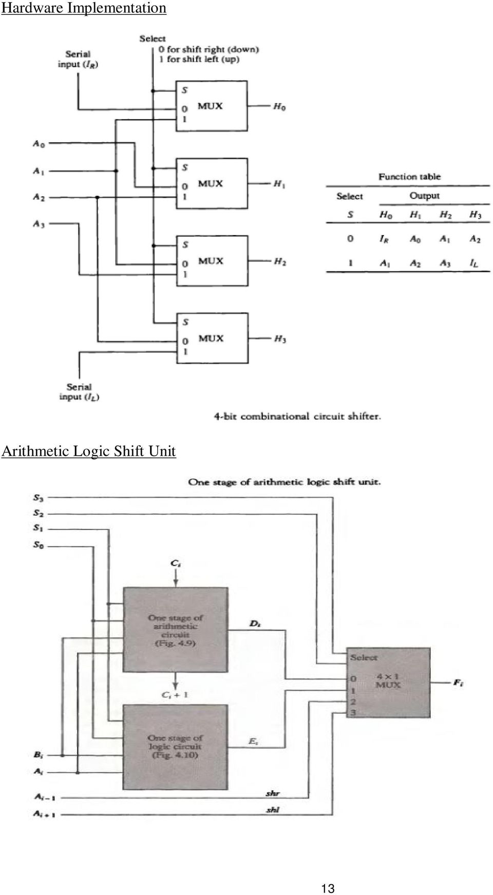
4 These conditions can be expressed by the following Boolean functions: A0 = D, + D3 + D5 + D7 A1 = D2 + D3 + D6 + D7 A2 = D4 + D5 + D6 + D7 Multiplexer: is a combinational circuit that receives binary information from one of 2" input data lines and directs it to a single output line. Registers register is a group of flip-flops with each flip-flop capable of storing one bit of information. An n-bit register has a group of n flip-flops and is capable of storing any binary information of n bits. Ex: 4 bit register Shift Registers A register capable of shifting its binary information in one or both directions is called a shift register. 4 bit shift register 4

5 Memory Unit A memory unit is a collection of storage cells together with associated circuits needed to transfer information in and out of storage. The memory stores binary word information in groups of bits called words. Random-Access Memory In random-access memory (RAM) the memory cells can be accessed for information transfer from any desired random location. Read-Only memory the name implies, a read-only memory (ROM) is a memory unit that performs the read operation only; it does not have a write capability. 5

6 Lecture 2: Register Transfer and Microoperations -Register Transfer Language Digital system: is an interconnection of digital hardware modules that accomplish a specific information-processing task. The modules are constructed from such digital components as registers, decoders, arithmetic elements, and control logic. The various modules are interconnected with common data and control paths to form a digital computer system. The operations executed on data stored in registers are called microoperations. A microoperation is an elementary operation performed on the information stored in one or more registers. The internal hardware organization of a digital computer is best defined by specifying: 1. The set of registers it contains and their function. 2. The sequence of microoperations performed on the binary information stored in the registers. 3. The control that initiates the sequence of microoperations. Registers transfer language: The symbolic notation used to describe the microoperation transfers register transfer among registers is called a register transfer language. The term registers transfer" implies the availability of hardware logic circuits that can perform a stated microoperation and transfer the result of the operation to the same or another register. Register Transfer Information transfer from one register to another is designated in symbolic form by means of a replacement operator. The statement R2 Rl denotes a transfer of the content of register Rl into register R2. It designates a replacement of the content of R2 by the content of Rl. By definition, the content of the source register Rl does not change after the transfer. 6

7 If we want the transfer to occur only under a predetermined control condition. This can be shown by means of an if-then statement. If (P = 1) then (R2 Rl) Control function It is sometimes convenient to separate the control variables from the register transfer operation by specifying a control function. P: R2 Rl Bus and Memory Transfers A typical digital computer has many registers, and paths must be provided to transfer information from one register to another. The number of wires will be excessive if separate lines are used between each register and all other registers in the system. A more efficient scheme for transferring information between common bus registers in a multiple-register configuration is a common bus system. 7

8 Three-State Bus Buffers: 8

9 Memory Transfer Read: DR M[AR] 9

10 Lecture 3: Binary Adder To implement the add microoperation with hardware, we need the registers that hold the data and the digital component that performs the arithmetic addition. Binary Adder-Subtractor The subtraction of binary numbers can be done most conveniently by means of complements Binary Incrementer Arithmetic Circuit The output of the binary adder is calculated from the following arithmetic sum: D = A + Y + Cin 10

11 11

12 Logic Microoperations Hardware Implementation Shift Microoperations 12

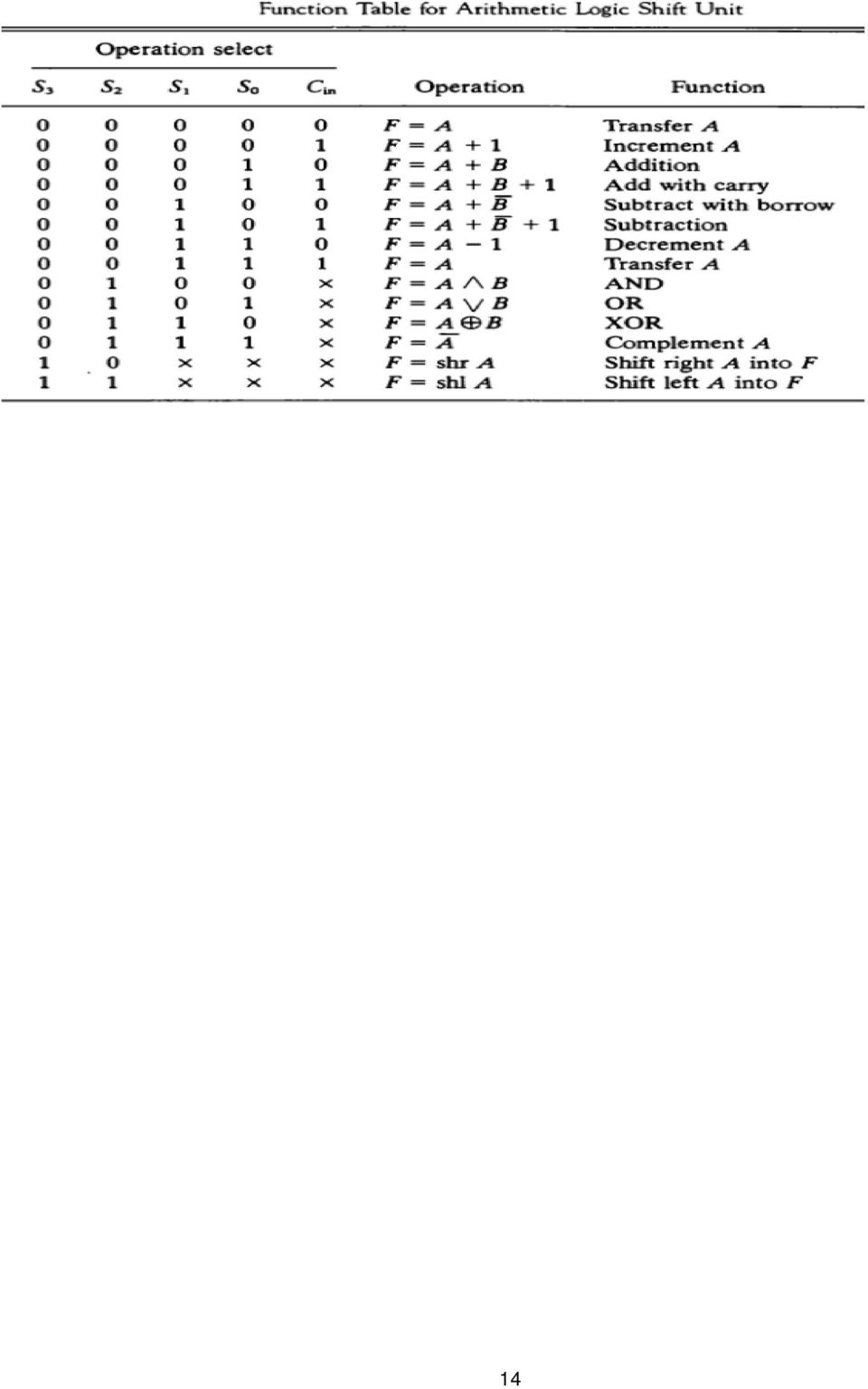
13 Hardware Implementation Arithmetic Logic Shift Unit 13
14 14
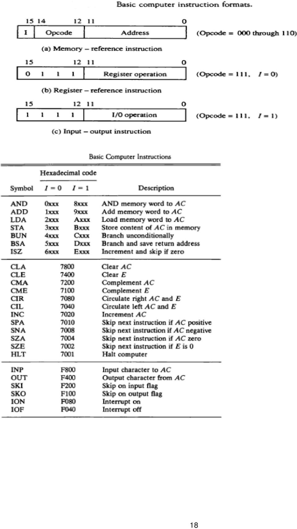
15 Lecture 4: Basic Computer Organization and Design Instruction code is a group of bits that instruct the computer to perform a specific operation. It is usually divided into parts, each having its own particular interpretation. The most basic part of an instruction code is its operation code operation part. Stored Program Organization -Computers that have a single-processor register usually assign to it the name accumulator (AC) and label it AC. Indirect Address:It is sometimes convenient to use the address bits of an instruction code not as an address but as the actual operand. When the second part of an instruction code specifies an operand, the instruction is said to have an immediate operand. The effective address to be the address of the operand in a computation-type instruction or the target address in a branch-type instruction. 15

16 Computer Registers -Computer instructions are normally stored in consecutive memory locations and are executed sequentially one at a time. Common Bus System Paths must be provided to transfer information from one register to another and between memory and registers. The number of wires will be excessive if connections are made between the outputs of each register and the inputs of the other registers. 16

17 - The input data and output data of the memory are connected to the common bus, but the memory address is connected to AR. - DR AC and AC DR - can be executed at the same time. This can be done by placing the content of AC on the bus (with S2SiS0 = 100), enabling the LD (load) input of DR, transferring the content of DR through the adder and logic circuit into AC, and enabling the LD (load) input of AC, all during the same clock cycle. The two transfers occur upon the arrival of the clock pulse transition at the end of the clock cycle. Computer Instructions The operation code (opcode) part of the instruction contains three bits and the meaning of the remaining 13 bits depends on the operation code encountered. A memory-reference instruction uses 12 bits to specify an address and one bit to specify the addressing mode J. 17
 part of the instruction contains three bits and the meaning of the remaining 13 bits depends on the operation code encountered.")
18 18
19 Lecture 5: Instruction Set Completeness The set of instructions are said to be complete if the computer includes a sufficient number of instructions in each of the following categories: 1. Arithmetic, logical, and shift instructions 2. Instructions for moving information to and from memory and processor registers 3. Program control instructions together with instructions that check status conditions 4. Input and output instructions Timing and Control The clock pulses are applied to all flip-flops and registers in the system, including the flip-flops and registers in the control unit. The clock pulses do not change the state of a register unless the register is enabled by a control signal. The control signals are generated in the control unit and provide control inputs for the multiplexers in the common bus, control inputs in processor registers, and microoperations for the accumulator. - In the hardwired organization, the control logic is implemented with gates, flip-flops, decoders, and other digital circuits. It has the advantage that it can be optimized to produce a fast mode of operation. - In the microprogrammed control, any required control changes or modifications can be done by updating the microprogram in control memory. - The sequence counter SC can be incremented or cleared synchronously. Most of the time, the counter is incremented to provide the sequence of timing signals out of the 4 x 16 decoder. 19

20 20

21 Lecture 6: Instruction Cycle: The steps that the control unit carries out in executing aprogram are: (1) Fetch the next instruction to be executed from memory. (2) Decode the opcode. (3) Read operand(s) from main memory, if any. (4) Execute the instruction and store results, if any. (5) Go to step 1. Fetch and Decode: Initially, the program counter PC is loaded with the address of the first instruction in the program. The sequence counter SC is cleared to 0, providing a decoded timing signal T0. After each clock pulse, SC is incremented by one, so that the timing signals go through a sequence T0, Tu T2, and so on. T0: AR PC T1: IR M[AR], PC PC + 1 T2: D0/..., D7 Decode IR(12-14), AR IR(O-ll), I 1R(15) Since only AR is connected to the address inputs of memory, it is necessary to transfer the address from PC to AR during the clock transition associated with timing signal T0. 21
22 - To provide the data path for the transfer of PC to AR we must apply timing signal T0 to achieve the following connection: 1. Place the content of PC onto the bus by making the bus selection inputs S2SiS0 equal to Transfer the content of the bus to AR by enabling the LD input of AR. The next clock transition initiates the transfer from PC to AR since T0 = 1. T1: IR M[AR], PC PC +1 - The microoperation for the indirect address condition can be symbolized by the register transfer statement AR M[AR]. - The three instruction types are subdivided into four separate paths. The selected operation is activated with the clock transition associated with timing signal T3. This can be symbolized as follows: D7'IT3: AR M[AR] D7'I'T3: Nothing D7I'T3: Execute a register-reference instruction D7IT3: Execute an input-output instruction 22
23 Lecture 7: Register-Reference Instructions Register-reference instructions are recognized by the control when D7 = 1 and 1 = 0. These instructions use bits 0 through 11 of the instruction code to specify one of 12 instructions. These 12 bits are available in IR(O-ll). They were also transferred to AR during time T2. Memory -Reference Instructions The effective address of the instruction is in the address register AR and was placed there during timing signal T2 when I = 0, or during timing signal T3 when I=1. AND to AC This is an instruction that performs the AND logic operation on pairs of bits in AC and the memory word specified by the effective address. D0T4: DR M[AR] D0T5: AC AC +DR, SC O ADD to AC 23
24 This instruction adds the content of the memory word specified by the effective address to the value of AC. The sum is transferred into AC and the output carry Cout is transferred to the (extended accumulator) flip-flop. D1T4: DR M[AR] D1Ts: AC AC + DR, E Cout, SC 0 LDA: Load to AC This instruction transfers the memory word specified by the effective address to AC. The microoperations needed to execute this instruction are D2T4: DR M[AR] D2T5: AC DR, SC 0 STA: Store AC This instruction stores the content of AC into the memory word specified by the effective address. D3T4: M[AR] AC, SC 0 BUN: Branch Unconditionally D4T4: PC AR, SC 0 BSA: Branch and Save Return Address D5T4: M[AR] PC, AR AR + 1 D5T5: PC AR, SC 0 ISZ: Increment and Skip if Zero D6T4: DR M[AR] 24
25 D6T5: DR DR + 1 D6T6: M[AR] DR, if (DR = 0) then (PC PC + 1), SC 0 Input Output and Interrupt - A computer can serve no useful purpose unless it communicates with the external environment. Instructions and data stored in memory must come from some input device. Input-Output Configuration Input-Output Instructions 25
26 Lecture 8: Program Interrupt - The process of communication just described is referred to as programmed control transfer. The computer keeps checking the flag bit, and when it finds it set, it initiates an information transfer. The difference of information flow rate between the computer and that of the input-output device makes this type of transfer inefficient. - To see why this is inefficient, consider a computer that can go through an instruction cycle in 1 (is. Assume that the input-output device can transfer information at a maximum rate of 10 characters per second. This is equivalent to one character every 100,000 µs. - An alternative to the programmed controlled procedure is to let the external device inform the computer when it is ready for the transfer. In the meantime the computer can be busy with other tasks. This type of transfer uses the interrupt facility. While the computer is running a program, it does not check the flags. 26
27 Interrupt Cycle T0'T1'T2'(IEN)(FGI + FGO): R 1 Can be done with the following sequence of microoperations: RT0: AR O, TR PC RT1: M[AR] TR, PC 0 RT2:PC PC + 1, IEN 0, R 0, SC 0 Design of Basic Computer The basic computer consists of the following hardware components: 1. A memory unit with 4096 words of 16 bits each 2. Nine registers: AR, PC, DR, AC, IR, TR, OUTR, INPR, and SC 3. Seven flip-flops: /, S, E, R, IEN, FGI, and FGO 4. Two decoders: a 3 x 8 operation decoder and a 4 x 16 timing decoder 5. A 16-bit common bus 6. Control logic gates 7. Adder and logic circuit connected to the input of AC 27
28 Control Logic Gates - The inputs to this circuit come from the two decoders, the J flip-flop, and bits 0 through 11 of IR. The other inputs to the control logic are: AC bits 0 through 15 to check if AC = 0 and to detect the sign bit in AC(15); DR bits 0 through 15 to check if DR = 0; and the values of the seven flip-flops. - The outputs of the control logic circuit are: 1. Signals to control the inputs of the nine registers 2. Signals to control the read and write inputs of memory 3. Signals to set, clear, or complement the flip-flops 4. Signals for S2, Si, and S0 to select a register for the bus 5. Signals to control the AC adder and logic circuit Control of Registers and Memory - The control inputs of the registers are LD (load), INR (increment), and CLR (clear). - Suppose that we want to derive the gate structure associated with the control inputs of AR. We scan Table 5-6 to find all the statements that change the content of AR: 28
29 R'T0: AR PC R'T2: AR IR(O-ll) D7'IT3: AR M[AR] RT0: AR O D5T4: AR AR + 1 The control functions can be combined into three Boolean expressions as follows: LD(AR) = R'T0 + R'T2 + D7'TT3 CLR(AR) = RT0 INR(AR) = D5T4 - In a similar fashion we can derive the control gates for the other registers as well as the logic needed to control the read and write inputs of memory. Read = R'T1+ D7'IT3 + (D0 + D1 + D2 + D6)T4 - The output of the logic gates that implement the Boolean expression above must be connected to the read input of memory. Control of Single Flip-flops - The control gates for the seven flip-flops can be determined in a similar manner. - EXAMPLE: IEN may change as a result of the two instructions ION and IOF. pb7: IEN 1 pb6: len O where p = D7IT3 and B7 and B6 are bits 7 and 6 of IR, respectively. Moreover, at the end of the interrupt cycle IEN is cleared to 0. RT2: IEN 0 29
30 Control of Common Bus So = X1 + x3 + x5 + x7 Si = x2 + x3 + x6 + x7 S2 = Xi + x5 + X6, + x7 - x7 = R'T1 + D7'IT3 + (D0 + D1 + D2 + D6)T4 Design of Accumulator Logic - In order to design the logic associated with AC, it is necessary to go over the register transfer statements and extract all the statements that change the content of AC. - - From this list we can derive the control logic gates and the adder and logic circuit. 30
31 Control of AC Register Adder and logic circuit - The adder and logic circuit can be subdivided into 16 stages, with each stage corresponding to one bit of AC. - One stage of the adder and logic circuit consists of seven AND gates, one OR gate and a fulladder (FA) 31
32 - 32
33 LECTURE 9: Central Processing Unit CPU:The part of the computer that performs the bulk of data-processing operations is called the central processing unit and is referred to as the CPU. The CPU is made up of three major parts: 1- The register set stores intermediate data used during the execution of the instructions. 2- The arithmetic logic unit (ALU) performs the required microoperations for executing the instructions. 3- The control unit supervises the transfer of information among the registers and instructs the ALU as to which operation to perform. General Register Organization The output of each register is connected to two multiplexers (MUX) to form the two buses A and B. The selection lines in each multiplexer select one register or the input data for the particular bus. 33
34 For example, to perform the operation R1 R2 + R3 The control must provide binary selection variables to the following selector inputs: 1. MUX A selector (SELA): to place the content of R2 into bus A. 2. MUX B selector (SELB): to place the content of R3 into bus B. 3. ALU operation selector (OPR): to provide the arithmetic addition A + B. 4. Decoder destination selector (SELD): to transfer the content of the output bus into Rl. Control Word There are 14 binary selection inputs in the unit, and their combined value specifies a control word. The encoding of the register selections is specified in following Table. The 3-bit binary code listed in the first column of the table specifies the binary code for each of the three fields. The register selected by fields SELA, SELB, and SELD is the one whose decimal number is equivalent to the binary number in the code. - The ALU provides arithmetic and logic operations. In addition, the CPU must provide shift operations. The shifter may be placed in the input of the ALU to provide a preshift capability, or at the output of the ALU to provide postshifting capability. 34
35 Lecture10: Stack Organization A stack is a storage device that stores information in such a manner that the item stored last is the first item retrieved. The operation of a stack can be compared to a stack of trays. The last tray placed on top of the stack is the first to be taken off. - The register that holds the address for the stack is called a stack pointer (SP) because its value always points at the top item in the stack. Register Stack - A stack can be placed in a portion of a large memory or it can be organized as a collection of a finite number of memory words or registers. Following figure shows the organization of a 64- word register stack. - Initially, SP is cleared to 0, EMTY is set to 1, and FULL is cleared to 0, so that SP points to the word at address 0 and the stack is marked empty and not full. If the stack is not full (if FULL = 0), a new item is inserted with a push operation. The push operation is implemented with the following sequence of microoperations: SP SP + 1 Increment stack pointer M[SP] DR Write item on top of the stack If (SP = 0) then (FULL 1) Check if stack is full EMTY 0 Mark the stack not empty - A new item is deleted from the stack if the stack is not empty (if pop EMTY = 0). The pop operation consists of the following sequence of micro- operations: 35
36 DR M[SP] SP SP - 1 If (SP = 0) then (EMTY 1) FULL 0 Read item from the top of stack Decrement stack pointer Check if stack is empty Mark the stack not full Memory Stack Following Figure shows a portion of computer memory partitioned into three segments: program, data, and stack. The program counter PC points at the address of the next instruction in the program. The address register AR points at an array of data. We assume that the items in the stack communicate with a data register DR. A new item is inserted with the push operation as follows: SP SP- 1 M[SP) DR The stack pointer is decremented so that it points at the address of the next word. A memory write operation inserts the word from DR into the top of the stack. A new item is deleted with a pop operation as follows: DR M[SP] SP SP
37 The top item is read from the stack into DR. The stack pointer is then incremented to point at the next item in the stack. - The advantage of a memory stack is that the CPU can refer to it without having to specify an address, since the address is always available and automatically updated in the stack pointer. Reverse Polish Notation - stack organization is very effective for evaluating arithmetic expressions. The common mathematical method of writing arithmetic expressions imposes difficulties when evaluated by a computer. The common arithmetic expressions are written in infix notation, with each operator written between the operands. Consider the simple arithmetic expression A*B + C*D - The Polish mathematician Lukasiewicz showed that arithmetic expressions can be represented in prefix notation. This representation, often referred to as Polish notation, places the operator before the operands. The postfix notation, referred to as reverse Polish notation (RPN), places the operator after the operands. The following examples demonstrate the three representations: A + B Infix notation +AB Prefix or Polish notation AB+ Postfix or reverse Polish notation - The reverse Polish notation is in a form suitable for stack manipulation. - The expression A*B + C*D is written in reverse Polish notation as AB*CD*+ Evaluation of Arithmetic Expressions - Reverse Polish notation, combined with a stack arrangement of registers, is the most efficient way known for evaluating arithmetic expressions. This procedure is employed in some electronic calculators and also in some computers. - The stack is particularly useful for handling long, complex problems involving chain calculations. It is based on the fact that any arithmetic expression can be expressed in parentheses-free Polish notation. - The following numerical example may clarify this procedure. Consider the arithmetic expression (3*4) + (5*6) In reverse Polish notation, it is expressed as 34*56* + - Scientific calculators that employ an internal stack require that the user convert the arithmetic expressions into reverse Polish notation. Computers that use a stack-organized CPU provide a system program to perform the conversion for the user. 37
38 Instruction Formats The format of an instruction is usually depicted in a rectangular box symbolizing the bits of the instruction as they appear in memory words or in a control register. The bits of the instruction are divided into groups called fields. The most common fields found in instruction formats are: 1. An operation code field that specifies the operation to be performed. 2. An address field that designates a memory address or a processor register. 3. A mode field that specifies the way the operand or the effective address is determined. - Operands residing in processor registers are specified with a register address. - Computers may have instructions of several different lengths containing varying number of addresses. The number of address fields in the instruction format of a computer depends on the internal organization of its registers. Most computers fall into one of three types of CPU organizations: 1. Single accumulator organization. 2. General register organization. 3. Stack organization. -- Three*Address Instructions Computers with three-address instruction formats can use each address field to specify either a processor register or a memory operand. The program in assembly language that evaluates X = (A + B) * (C + D) is shown below, together with comments that explain the register transfer operation of each instruction. ADD Rl, A, B ADD R2, C, D MUL X, Rl, R2 R1 M[A]+M[B] R2 M[C]+M[D] M[X] R1*R2 from memory and AC register. We will assume that the operands are in memory addresses A, B, C, and D, and the result must be stored in memory at address X. Three*Address Instructions 38
39 Computers with three-address instruction formats can use each address field to specify either a processor register or a memory operand. The program in assembly language that evaluates X = (A + B) * (C + D) is shown below, together with comments that explain the register transfer operation of each instruction. ADD Rl, A, B R1^M[A]+M[B] ADD RE, C, D RE^M[C]+M[D] MUL X, Rl, RE M[X]^R1*RE It is assumed that the computer has two processor registers, Rl and R2. The symbol M[A] denotes the operand at memory address symbolized by A. The advantage of the three-address format is that it results in short programs when evaluating arithmetic expressions. The disadvantage is that the binarycoded instructions require too many bits to specify three addresses. An example of a commercial computer that uses three-address instructions is the Cyber 170. The instruction formats in the Cyber computer are restricted to either three register address fields or two register address fields and one memory address field. ---Two'Address Instructions Two-address instructions are the most common in commercial computers. Here again each address field can specify either a processor register or a memory word. The program to evaluate X = (A + B) * (C + D) is as follows: MOV Rl, A ADD Rl, B MOV R2, C ADD R2,D MUL Rl,R2 MOV X, R1 R1 M[A] Rl Rl + M[B] R2 M[C] R2 R2 + M[D] R1 R1*R2 M[X] R1 --One'Address Instructions One-address instructions use an implied accumulator (AC) register for all data manipulation. For multiplication and division there is a need for a second register. However, here we will neglect the second register and assume that the AC contains the result of all operations. The program to evaluate X = (A + B)*(C + D)is 39
40 --Zero'Address Instructions A stack-organized computer does not use an address held for the instructions ADD and MUL. The PUSH and POP instructions, however, need an address held to specify the operand that communicates with the stack. The following program shows how X = (A + B) * (C + D) will be written for a stackorganized computer. (TOS stands for top of stack.) --RISC Instructions The instruction set of a typical RISC processor is restricted to the use of load and store instructions when communicating between memory and CPU. All other instructions are executed within the registers of the CPU without referring to memory. The following is a program to evaluate X = (A + B)*(C + D). 40
41 Lecture11: Addressing Modes The operation field of an instruction specifies the operation to be performed. This operation must be executed on some data stored in computer registers or memory words. Computers use addressing mode techniques for the purpose of accommodating one or both of the following provisions: 1. To give programming versatility to the user by providing such facilities as pointers to memory, counters for loop control, indexing of data, and program relocation. 2. To reduce the number of bits in the addressing field of the instruction. - The control unit of a computer is designed to go through an instruction cycle that is divided into three major phases: 1. Fetch the instruction from memory. 2. Decode the instruction. 3. Execute the instruction. - There is one register in the computer called the program counter or PC that keeps track of the instructions in the program stored in memory. PC holds the address of the instruction to be executed next and is incremented each time an instruction is fetched from memory. - The mode field is used to locate the operands needed for the operation. - Implied Mode: In this mode the operands are specified implicitly in the definition of the instruction. For example, the instruction "complement accumulator" is an implied-mode instruction because the operand in the accumulator register is implied in the definition of the instruction. In fact, all register reference instructions that use an accumulator are implied-mode instructions. - Immediate Mode: In this mode the operand is specified in the instruction itself. Register Mode: In this mode the operands are in registers that reside within the CPU. The particular register is selected from a register field in the instruction. A k-bit field can specify any one of 2* registers. Register Indirect Mode: In this mode the instruction specifies a register in the CPU whose contents give the address of the operand in memory. Autoincrement or Autodecrement Mode: This is similar to the register indirect mode except that the register is incremented or decremented after (or before) its value is used to access memory. The effective address is defined to be the memory address obtained from the computation dictated by the given addressing mode. Direct Address Mode: In this mode the effective address is equal to the address part of the instruction. The operand resides in memory and its address is given directly by the address field of the instruction. 41
42 Indirect Address Mode: In this mode the address field of the instruction gives the address where the effective address is stored in memory. --- A few addressing modes require that the address field of the instruction be added to the content of a specific register in the CPU. The effective address in these modes is obtained from the following computation: effective address = address part of instruction + content of CPU register Relative Address Mode: In this mode the content of the program counter is added to the address part of the instruction in order to obtain the effective address. Indexed Addressing Mode: In this mode the content of an index register is added to the address part of the instruction to obtain the effective address. The index register is a special CPU register that contains an index value. The address field of the instruction defines the beginning address of a data array in memory. Base Register Addressing Mode: In this mode the content of a base register is added to the address part of the instruction to obtain the effective address. This is similar to the indexed addressing mode except that the register is now called a base register instead of an index register. 42
43 Lecture12: Data Transfer and Manipulation The instruction set of different computers differ from each other mostly in the way the operands are determined from the address and mode fields. Most computer instructions can be classified into three categories: 1. Data transfer instructions 2. Data manipulation instructions 3. Program control instructions Data transfer instructions cause transfer of data from one location to another without changing the binary information content. Data manipulation instructions are those that perform arithmetic, logic, and shift operations. Program control instructions provide decision-making capabilities and change the path taken by the program when executed in the computer. Data Transfer Instructions - Data transfer instructions move data from one place in the computer to another without changing the data content. The most common transfers are between memory and processor registers, between processor registers and input or output, and between the processor registers themselves. Data Manipulation Instructions - Data manipulation instructions perform operations on data and provide the computational capabilities for the computer. The data manipulation instructions in a typical computer are usually divided into three basic types: 1. Arithmetic instructions 2. Logical and bit manipulation instructions 3. Shift instructions Arithmetic Instructions The four basic arithmetic operations are addition, subtraction, multiplication, and division. Most computers provide instructions for all four operations. 43
44 Logical and Bit Manipulation Instructions Logical instructions perform binary operations on strings of bits stored in registers. They are useful for manipulating individual bits or a group of bits that represent binary-coded information. Shift Instructions Instructions to shift the content of an operand are quite useful and are often provided in several variations. Program Control Instructions are always stored in successive memory locations. When processed in the CPU, the instructions are fetched from consecutive memory locations and executed. 44
45 Status Bit Conditions It is sometimes convenient to supplement the ALU circuit in the CPU with a status register where status bit conditions can be stored for further analysis. Status bits are also called condition-code bits or flag bits. The four status bits are symbolized by C, S, Z, and V. The bits are set or cleared as a result of an operation performed in the ALU. 1. Bit C (carry) is set to 1 if the end cany C8 is 1. It is cleared to 0 if the cany iso. 2. Bit S (sign) is set to 1 if the highest-order bit F? is 1. It is set to 0 if the bit is Bit Z (zero) is set to 1 if the output of the ALU contains all 0's. It is cleared to 0 otherwise. In other words, Z = 1 if the output is zero and Z = 0 if the output is not zero. 4. Bit V (overflow) is set to 1 if the exclusive-or of the last two carries is equal to 1, and cleared to 0 otherwise. This is the condition for an overflow when negative numbers are in 2's complement. For the 8-bit ALU, V = 1 if the output is greater than +127 or less than
46 Conditional Branch Instructions - Some computers consider the C bit to be a borrow bit after a subtraction operation A B. A borrow does not occur if A ^ B, but a bit must be borrowed from the next most significant position if A < B. The condition for a borrow is the complement of the carry obtained when the subtraction is done by taking the 2's complement of B. For this reason, a processor that considers the C bit to be a borrow after a subtraction will complement the C bit after adding the 2's complement of the subtrahend and denote this bit a borrow. Subroutine Call and Return - A subroutine is a self-contained sequence of instructions that performs a given computational task. - The instruction that transfers program control to a subroutine is known by different names. The most common names used are call subroutine, jump to subroutine, branch to subroutine, or branch and save address. - The instruction is executed by performing two operations: (1) the address of the next instruction available in the program counter (the return address) is stored in a temporary location so the subroutine knows where to return (2) control is transferred to the beginning of the subroutine. Different computers use a different temporary location for storing the return address. - Some store the return address in the first memory location of the subroutine, some store it in a fixed location in memory, some store it in a processor register, and some store it in a memory stack. The most efficient way is to store the return address in a memory stack. The advantage of 46
47 using a stack for the return address is that when a succession of subroutines is called, the sequential return addresses can be pushed into the stack. The return from subroutine instruction causes the stack to pop and the contents of the top of the stack are transferred to the program counter. - A subroutine call is implemented with the following microoperations: SP SP - 1 Decrement stack pointer M[SP] PC Push content of PC onto the stack PC effective address Transfer control to the subroutine - If another subroutine is called by the current subroutine, the new return address is pushed into the stack, and so on. The instruction that returns from the last subroutine is implemented by the microoperations: PC M[SP] Pop stack and transfer to PC SP SP + 1 Increment stack pointer 47
48 Lecture13: Program Interrupt - Program interrupt refers to the transfer of program control from a currently running program to another service program as a result of an external or internal generated request. Control returns to the original program after the service program is executed. - The interrupt procedure is, in principle, quite similar to a subroutine call except for three variations: (1) The interrupt is usually initiated by an internal or external signal rather than from the execution of an instruction (except for software interrupt as explained later); (2) the address of the interrupt service program is determined by the hardware rather than from the address field of an instruction; and (3) an interrupt procedure usually stores all the information - The state of the CPU at the end of the execute cycle (when the interrupt is recognized) is determined from: 1. The content of the program counter 2. The content of all processor registers 3. The content of certain status conditions - program status word The collection of all status bit conditions in the CPU is sometimes called a program status word or PSW. The PSW is stored in a separate hardware register and contains the status information that characterizes the state of the CPU. Types of Interrupts - There are three major types of interrupts that cause a break in the normal execution of a program. They can be classified as: 1. External interrupts 2. Internal interrupts 3. Software interrupts - External interrupts come from input-output (I/O) devices, from a timing device, from a circuit monitoring the power supply, or from any other external source. - Internal interrupts arise from illegal or erroneous use of an instruction or data. Internal interrupts are also called traps. Examples of interrupts caused by internal error conditions are register overflow, attempt to divide by zero, an invalid operation code, stack overflow, and protection violation. - A software interrupt is initiated by executing an instruction. Software interrupt is a special call instruction that behaves like an interrupt rather than a subroutine call. It can be used by the programmer to initiate an interrupt procedure at any desired point in the program. Reduced Instruction Set Computer (RISC) 48
49 - An important aspect of computer architecture is the design of the instruction set for the processor. The instruction set chosen for a particular computer determines the way that machine language programs are constructed. - A computer with a large number of instructions is classified as a complex instruction set computer, abbreviated CISC. - In the early 1980s, a number of computer designers recommended that - Computers use fewer instructions with simple constructs so they can be executed much faster within the CPU without having to use memory as often. This type of computer is classified as a reduced instruction set computer or RISC. CISC Characteristics - The design of an instruction set for a computer must take into consideration not only machine language constructs, but also the requirements imposed on the use of high-level programming languages. - the major characteristics of CISC architecture are: 1. A large number of instructions typically from 100 to 250 instructions 2, Some instructions that perform specialized tasks and are used infrequently. 3. A large variety of addressing modes typically from 5 to 20 different modes 4. Variable-length instruction formats 5. Instructions that manipulate operands in memory RISC Characteristics - The concept of RISC architecture involves an attempt to reduce execution time by simplifying the instruction set of the computer. The major characteristics of a RISC processor are: 1. Relatively few instructions 2. Relatively few addressing modes 3. Memory access limited to load and store instructions 4. All operations done within the registers of the CPU 5. Fixed-length, easily decoded instruction format 6. Single-cycle instruction execution 7. Hardwired rather than microprogrammed control - Other characteristics attributed to RISC architecture are: 1. A relatively large number of registers in the processor unit 2. Use of overlapped register windows to speed-up procedure call and return 3. Efficient instruction pipeline 4. Compiler support for efficient translation of high-level language programs into machine language programs. Overlapped Register Windows - Procedure call and return occurs quite often in high-level programming languages. When translated into machine language, a procedure call produces a sequence of instructions that save 49
50 register values, pass parameters needed for the procedure, and then calls a subroutine to execute the body of the procedure. - A characteristic of some RISC processors is their use of overlapped register windows to provide the passing of parameters and avoid the need for saving and restoring register values. - The system has a total of 74 registers. Registers RO through R9 are global registers that hold parameters shared by all procedures. The other 64 registers are divided into four windows to accommodate procedures A,B,C, and D. Each register window consists of 10 local registers and two sets of six registers common to adjacent windows. Local registers are used for local variables. - In general, the organization of register windows will have the following relationships: number of global registers = G number of local registers in each window = L number of registers common to two windows = C number of windows = W - The number of registers available for each window is calculated as follows: window size = L + 2C + G The total number of registers needed in the processor is register file = (L + C)W + G In the example of Fig above we have G = 10, L = 10, C = 6, and W = 4. The window size is = 32 registers, and the register file consists of (10 + 6) x = 74 registers. 50
51 Lecture14: Microprogrammed Control(Control Unit) Control Memory Control Unit Initiate sequences of microoperations Control signal (that specify microoperations) in a bus-organized systemgroups of bits that select the paths in multiplexers, decoders, and arithmetic logic units Two major types of Control Unit - Hardwired Control : The control logic is implemented with gates, F/Fs, decoders, and other digital circuits - Fast operation, - Wiring change(if the design has to be modified) - Microprogrammed Control : The control information is stored in a control memory, and the control memory is programmed to initiate the required sequence of microoperations + Any required change can be done by updating the microprogram in control memory, - Slow operation Control Word The control variables at any given time can be represented by a string of 1 s and 0 s. Microprogrammed Control Unit A control unit whose binary control variables are stored in memory (control memory). - Microinstruction : Control Word in Control Memory The microinstruction specifies one or more microoperations - Microprogram :A sequence of microinstruction Dynamic microprogramming : Control Memory = RAM - RAM can be used for writing (to change a writable control memory) - Microprogram is loaded initially from an auxiliary memory such as a magnetic disk Static microprogramming : Control Memory = ROM - Control words in ROM are made permanent during the hardware production. Microprogrammed control Organization : 1) Control Memory - A memory is part of a control unit : Microprogram - Computer Memory (employs a microprogrammed control unit) Main Memory : for storing user program (Machine instruction/data) Control Memory : for storing microprogram (Microinstruction) 2) Control Address Register Specify the address of the microinstruction 3) Sequencer (= Next Address Generator) Determine the address sequence that is read from control memory Next address of the next microinstruction can be specified several way depending on the sequencer input 4) Control Data Register (= Pipeline Register ) 51
52 Hold the microinstruction read from control memory Allows the execution of the microoperations specified by the control word simultaneously with the generation of the next microinstruction - RISC Architecture Concept RISC(Reduced Instruction Set Computer) system use hardwired control rather than microprogrammed control - Address Sequencing - Address Sequencing = Sequencer : Next Address Generator Selection of address for control memory - Routine Microinstruction are stored in control memory in groups - Mapping Instruction Code Address in control memory(where routine is located) - Address Sequencing Capabilities : control memory address 1) Incrementing of the control address register 2) Unconditional branch or conditional branch, depending on status bit conditions 3) Mapping process ( bits of the instruction address for control memory ) 4) A facility for subroutine return - Selection of address for control memory : Multiplexer CAR Increment JMP/CALL Mapping Subroutine Return CAR : Control Address Register. CAR receive the address from 4different paths 1) Incrementer 2) Branch address from control memory 3) Mapping Logic 4) SBR : Subroutine Register,SBR : Subroutine Register(Return Address can not be stored in ROM) Instruction code Mapping logic Status bits Branch logic MUX select Multiplexers Clock Control address register (CAR) Subroutine regiser (SBR) Incrementer 52 Control memory Select a status bit Microoperations Branch address
53 Conditional Branching Status Bits» Control the conditional branch decisions generated in the Branch Logic Branch Logic» Test the specified condition and Branch to the indicated address if the condition is met ; otherwise, the control address register is just incremented. Status Bit Test 와 Branch Logic» 4 X 1 Mux 와 Input Logic Mapping of Instruction : 4 bit Opcode = specify up to 16 distinct instruction Mapping Process : Converts the 4-bit Opcode to a 7-bit control memory address» 1) Place a 0 in the most significant bit of the address» 2) Transfer 4-bit Operation code bits» 3) Clear the two least significant bits of the CAR (Microinstruction) Mapping Function : Implemented by Mapping ROM or PLD Control Memory Size : 128 words (= 2 7 ) Subroutine Subroutines are programs that are used by other routines - Subroutine can be called from any point within the main body of the microprogram Microinstructions can be saved by subroutines that use common section of microcode ) Memory Reference, Operand, Effective Address Subroutine Subroutine은 ORG 64, 즉 에 위치(Routine은 ) Subroutine must have a provision for» storing the return address during a subroutine call» restoring the address during a subroutine return Last-In First Out(LIFO) Register Stack 53
54 Lecture15: Microprogram Example Computer Configuration : 2 Memory : Main memory(instruction/data), Control memory(microprogram)» Data written to memory come from DR, and Data read from memory can go only to DR 4 CPU Register and ALU : DR, AR, PC, AC, ALU» DR can receive information from AC, PC, or Memory (selected by MUX)» AR can receive information from PC or DR (selected by MUX)» PC can receive information only from AR» ALU performs microoperation with data from AC and DR 2 Control Unit Register : SBR, CAR Instruction Format Instruction Format :» I : 1 bit for indirect addressing» Opcode : 4 bit operation code» Address : 11 bit address for system memory Computer Instruction : Microinstruction Format : 3 bit Microoperation Fields : F1, F2, F3» 총 21개 Microoperation :» 3 microoperation 3, 000(no operation)» two or more conflicting microoperations can not be specified simultaneously) Clear AC to 0 and subtract DR from AC at the same time» Symbol DRTAC(F1 = 100) stand for a transfer from DR to AC (T = to) MUX 10 0 AR 10 0 PC Address Memory MUX SBR CAR 15 0 DR Control memory Control unit 54 Arithmetic logic and shift unit 15 0 AC
BASIC COMPUTER ORGANIZATION AND DESIGN
 1 BASIC COMPUTER ORGANIZATION AND DESIGN Instruction Codes Computer Registers Computer Instructions Timing and Control Instruction Cycle Memory Reference Instructions Input-Output and Interrupt Complete
Chapter 4 Register Transfer and Microoperations. Section 4.1 Register Transfer Language
 Chapter 4 Register Transfer and Microoperations Section 4.1 Register Transfer Language Digital systems are composed of modules that are constructed from digital components, such as registers, decoders,
Advanced Computer Architecture-CS501. Computer Systems Design and Architecture 2.1, 2.2, 3.2
 Lecture Handout Computer Architecture Lecture No. 2 Reading Material Vincent P. Heuring&Harry F. Jordan Chapter 2,Chapter3 Computer Systems Design and Architecture 2.1, 2.2, 3.2 Summary 1) A taxonomy of
Central Processing Unit (CPU)
") Central Processing Unit (CPU) CPU is the heart and brain It interprets and executes machine level instructions Controls data transfer from/to Main Memory (MM) and CPU Detects any errors In the following
Central Processing Unit (CPU) CPU is the heart and brain It interprets and executes machine level instructions Controls data transfer from/to Main Memory (MM) and CPU Detects any errors In the following
Systems I: Computer Organization and Architecture
 Systems I: Computer Organization and Architecture Lecture 9 - Register Transfer and Microoperations Microoperations Digital systems are modular in nature, with modules containing registers, decoders, arithmetic
MICROPROCESSOR AND MICROCOMPUTER BASICS
 Introduction MICROPROCESSOR AND MICROCOMPUTER BASICS At present there are many types and sizes of computers available. These computers are designed and constructed based on digital and Integrated Circuit
Chapter 2 Basic Structure of Computers. Jin-Fu Li Department of Electrical Engineering National Central University Jungli, Taiwan
 Chapter 2 Basic Structure of Computers Jin-Fu Li Department of Electrical Engineering National Central University Jungli, Taiwan Outline Functional Units Basic Operational Concepts Bus Structures Software
Systems I: Computer Organization and Architecture
 Systems I: Computer Organization and Architecture Lecture : Microprogrammed Control Microprogramming The control unit is responsible for initiating the sequence of microoperations that comprise instructions.
CHAPTER 7: The CPU and Memory
 CHAPTER 7: The CPU and Memory The Architecture of Computer Hardware, Systems Software & Networking: An Information Technology Approach 4th Edition, Irv Englander John Wiley and Sons 2010 PowerPoint slides
Chapter 2 Logic Gates and Introduction to Computer Architecture
 Chapter 2 Logic Gates and Introduction to Computer Architecture 2.1 Introduction The basic components of an Integrated Circuit (IC) is logic gates which made of transistors, in digital system there are
MACHINE ARCHITECTURE & LANGUAGE
 in the name of God the compassionate, the merciful notes on MACHINE ARCHITECTURE & LANGUAGE compiled by Jumong Chap. 9 Microprocessor Fundamentals A system designer should consider a microprocessor-based
MICROPROCESSOR. Exclusive for IACE Students www.iace.co.in iacehyd.blogspot.in Ph: 9700077455/422 Page 1
 MICROPROCESSOR A microprocessor incorporates the functions of a computer s central processing unit (CPU) on a single Integrated (IC), or at most a few integrated circuit. It is a multipurpose, programmable
(Refer Slide Time: 00:01:16 min)
") Digital Computer Organization Prof. P. K. Biswas Department of Electronic & Electrical Communication Engineering Indian Institute of Technology, Kharagpur Lecture No. # 04 CPU Design: Tirning & Control
Digital Computer Organization Prof. P. K. Biswas Department of Electronic & Electrical Communication Engineering Indian Institute of Technology, Kharagpur Lecture No. # 04 CPU Design: Tirning & Control
Chapter 5 Instructor's Manual
 The Essentials of Computer Organization and Architecture Linda Null and Julia Lobur Jones and Bartlett Publishers, 2003 Chapter 5 Instructor's Manual Chapter Objectives Chapter 5, A Closer Look at Instruction
A single register, called the accumulator, stores the. operand before the operation, and stores the result. Add y # add y from memory to the acc
 Other architectures Example. Accumulator-based machines A single register, called the accumulator, stores the operand before the operation, and stores the result after the operation. Load x # into acc
Computer organization
 Computer organization Computer design an application of digital logic design procedures Computer = processing unit + memory system Processing unit = control + datapath Control = finite state machine inputs
LSN 2 Computer Processors
 LSN 2 Computer Processors Department of Engineering Technology LSN 2 Computer Processors Microprocessors Design Instruction set Processor organization Processor performance Bandwidth Clock speed LSN 2
CHAPTER 4 MARIE: An Introduction to a Simple Computer
 CHAPTER 4 MARIE: An Introduction to a Simple Computer 4.1 Introduction 195 4.2 CPU Basics and Organization 195 4.2.1 The Registers 196 4.2.2 The ALU 197 4.2.3 The Control Unit 197 4.3 The Bus 197 4.4 Clocks
1 Classical Universal Computer 3
 Chapter 6: Machine Language and Assembler Christian Jacob 1 Classical Universal Computer 3 1.1 Von Neumann Architecture 3 1.2 CPU and RAM 5 1.3 Arithmetic Logical Unit (ALU) 6 1.4 Arithmetic Logical Unit
2) Write in detail the issues in the design of code generator.
 Write in detail the issues in the design of code generator.") COMPUTER SCIENCE AND ENGINEERING VI SEM CSE Principles of Compiler Design Unit-IV Question and answers UNIT IV CODE GENERATION 9 Issues in the design of code generator The target machine Runtime Storage
COMPUTER SCIENCE AND ENGINEERING VI SEM CSE Principles of Compiler Design Unit-IV Question and answers UNIT IV CODE GENERATION 9 Issues in the design of code generator The target machine Runtime Storage
150127-Microprocessor & Assembly Language
 Chapter 3 Z80 Microprocessor Architecture The Z 80 is one of the most talented 8 bit microprocessors, and many microprocessor-based systems are designed around the Z80. The Z80 microprocessor needs an
MACHINE INSTRUCTIONS AND PROGRAMS
 CHAPTER 2 MACHINE INSTRUCTIONS AND PROGRAMS CHAPTER OBJECTIVES In this chapter you will learn about: Machine instructions and program execution, including branching and subroutine call and return operations
CHAPTER 3 Boolean Algebra and Digital Logic
 CHAPTER 3 Boolean Algebra and Digital Logic 3.1 Introduction 121 3.2 Boolean Algebra 122 3.2.1 Boolean Expressions 123 3.2.2 Boolean Identities 124 3.2.3 Simplification of Boolean Expressions 126 3.2.4
PART B QUESTIONS AND ANSWERS UNIT I
 PART B QUESTIONS AND ANSWERS UNIT I 1. Explain the architecture of 8085 microprocessor? Logic pin out of 8085 microprocessor Address bus: unidirectional bus, used as high order bus Data bus: bi-directional
PROBLEMS (Cap. 4 - Istruzioni macchina)
") 98 CHAPTER 2 MACHINE INSTRUCTIONS AND PROGRAMS PROBLEMS (Cap. 4 - Istruzioni macchina) 2.1 Represent the decimal values 5, 2, 14, 10, 26, 19, 51, and 43, as signed, 7-bit numbers in the following binary
98 CHAPTER 2 MACHINE INSTRUCTIONS AND PROGRAMS PROBLEMS (Cap. 4 - Istruzioni macchina) 2.1 Represent the decimal values 5, 2, 14, 10, 26, 19, 51, and 43, as signed, 7-bit numbers in the following binary
Let s put together a Manual Processor
 Lecture 14 Let s put together a Manual Processor Hardware Lecture 14 Slide 1 The processor Inside every computer there is at least one processor which can take an instruction, some operands and produce
Instruction Set Architecture
 Instruction Set Architecture Consider x := y+z. (x, y, z are memory variables) 1-address instructions 2-address instructions LOAD y (r :=y) ADD y,z (y := y+z) ADD z (r:=r+z) MOVE x,y (x := y) STORE x (x:=r)
1. True or False? A voltage level in the range 0 to 2 volts is interpreted as a binary 1.
 File: chap04, Chapter 04 1. True or False? A voltage level in the range 0 to 2 volts is interpreted as a binary 1. 2. True or False? A gate is a device that accepts a single input signal and produces one
Digital Logic Design. Basics Combinational Circuits Sequential Circuits. Pu-Jen Cheng
 Digital Logic Design Basics Combinational Circuits Sequential Circuits Pu-Jen Cheng Adapted from the slides prepared by S. Dandamudi for the book, Fundamentals of Computer Organization and Design. Introduction
İSTANBUL AYDIN UNIVERSITY
 İSTANBUL AYDIN UNIVERSITY FACULTY OF ENGİNEERİNG SOFTWARE ENGINEERING THE PROJECT OF THE INSTRUCTION SET COMPUTER ORGANIZATION GÖZDE ARAS B1205.090015 Instructor: Prof. Dr. HASAN HÜSEYİN BALIK DECEMBER
Central Processing Unit
 Chapter 4 Central Processing Unit 1. CPU organization and operation flowchart 1.1. General concepts The primary function of the Central Processing Unit is to execute sequences of instructions representing
5 Combinatorial Components. 5.0 Full adder. Full subtractor
 5 Combatorial Components Use for data transformation, manipulation, terconnection, and for control: arithmetic operations - addition, subtraction, multiplication and division. logic operations - AND, OR,
CPU Organisation and Operation
 CPU Organisation and Operation The Fetch-Execute Cycle The operation of the CPU 1 is usually described in terms of the Fetch-Execute cycle. 2 Fetch-Execute Cycle Fetch the Instruction Increment the Program
An Overview of Stack Architecture and the PSC 1000 Microprocessor
 An Overview of Stack Architecture and the PSC 1000 Microprocessor Introduction A stack is an important data handling structure used in computing. Specifically, a stack is a dynamic set of elements in which
CPU Organization and Assembly Language
 COS 140 Foundations of Computer Science School of Computing and Information Science University of Maine October 2, 2015 Outline 1 2 3 4 5 6 7 8 Homework and announcements Reading: Chapter 12 Homework:
8085 INSTRUCTION SET
 DATA TRANSFER INSTRUCTIONS Opcode Operand Description 8085 INSTRUCTION SET INSTRUCTION DETAILS Copy from source to destination OV Rd, Rs This instruction copies the contents of the source, Rs register
A s we saw in Chapter 4, a CPU contains three main sections: the register section,
 6 CPU Design A s we saw in Chapter 4, a CPU contains three main sections: the register section, the arithmetic/logic unit (ALU), and the control unit. These sections work together to perform the sequences
Digital Electronics Detailed Outline
 Digital Electronics Detailed Outline Unit 1: Fundamentals of Analog and Digital Electronics (32 Total Days) Lesson 1.1: Foundations and the Board Game Counter (9 days) 1. Safety is an important concept
Instruction Set Architecture (ISA)
") Instruction Set Architecture (ISA) * Instruction set architecture of a machine fills the semantic gap between the user and the machine. * ISA serves as the starting point for the design of a new machine
Instruction Set Architecture (ISA) * Instruction set architecture of a machine fills the semantic gap between the user and the machine. * ISA serves as the starting point for the design of a new machine
Computer Organization and Architecture
 Computer Organization and Architecture Chapter 11 Instruction Sets: Addressing Modes and Formats Instruction Set Design One goal of instruction set design is to minimize instruction length Another goal
UNIVERSITY OF CALIFORNIA, DAVIS Department of Electrical and Computer Engineering. EEC180B Lab 7: MISP Processor Design Spring 1995
 UNIVERSITY OF CALIFORNIA, DAVIS Department of Electrical and Computer Engineering EEC180B Lab 7: MISP Processor Design Spring 1995 Objective: In this lab, you will complete the design of the MISP processor,
CS101 Lecture 26: Low Level Programming. John Magee 30 July 2013 Some material copyright Jones and Bartlett. Overview/Questions
 CS101 Lecture 26: Low Level Programming John Magee 30 July 2013 Some material copyright Jones and Bartlett 1 Overview/Questions What did we do last time? How can we control the computer s circuits? How
How It All Works. Other M68000 Updates. Basic Control Signals. Basic Control Signals
 CPU Architectures Motorola 68000 Several CPU architectures exist currently: Motorola Intel AMD (Advanced Micro Devices) PowerPC Pick one to study; others will be variations on this. Arbitrary pick: Motorola
Chapter 1 Computer System Overview
 Operating Systems: Internals and Design Principles Chapter 1 Computer System Overview Eighth Edition By William Stallings Operating System Exploits the hardware resources of one or more processors Provides
An Introduction to the ARM 7 Architecture
 An Introduction to the ARM 7 Architecture Trevor Martin CEng, MIEE Technical Director This article gives an overview of the ARM 7 architecture and a description of its major features for a developer new
a storage location directly on the CPU, used for temporary storage of small amounts of data during processing.
 CS143 Handout 18 Summer 2008 30 July, 2008 Processor Architectures Handout written by Maggie Johnson and revised by Julie Zelenski. Architecture Vocabulary Let s review a few relevant hardware definitions:
Counters and Decoders
 Physics 3330 Experiment #10 Fall 1999 Purpose Counters and Decoders In this experiment, you will design and construct a 4-bit ripple-through decade counter with a decimal read-out display. Such a counter
Instruction Set Architecture. or How to talk to computers if you aren t in Star Trek
 Instruction Set Architecture or How to talk to computers if you aren t in Star Trek The Instruction Set Architecture Application Compiler Instr. Set Proc. Operating System I/O system Instruction Set Architecture
A3 Computer Architecture
 A3 Computer Architecture Engineering Science 3rd year A3 Lectures Prof David Murray david.murray@eng.ox.ac.uk www.robots.ox.ac.uk/ dwm/courses/3co Michaelmas 2000 1 / 1 6. Stacks, Subroutines, and Memory
Instruction Set Design
 Instruction Set Design Instruction Set Architecture: to what purpose? ISA provides the level of abstraction between the software and the hardware One of the most important abstraction in CS It s narrow,
Modeling Sequential Elements with Verilog. Prof. Chien-Nan Liu TEL: 03-4227151 ext:34534 Email: jimmy@ee.ncu.edu.tw. Sequential Circuit
 Modeling Sequential Elements with Verilog Prof. Chien-Nan Liu TEL: 03-4227151 ext:34534 Email: jimmy@ee.ncu.edu.tw 4-1 Sequential Circuit Outputs are functions of inputs and present states of storage elements
Sistemas Digitais I LESI - 2º ano
 Sistemas Digitais I LESI - 2º ano Lesson 6 - Combinational Design Practices Prof. João Miguel Fernandes (miguel@di.uminho.pt) Dept. Informática UNIVERSIDADE DO MINHO ESCOLA DE ENGENHARIA - PLDs (1) - The
Administrative Issues
 CSC 3210 Computer Organization and Programming Introduction and Overview Dr. Anu Bourgeois (modified by Yuan Long) Administrative Issues Required Prerequisites CSc 2010 Intro to CSc CSc 2310 Java Programming
DEPARTMENT OF COMPUTER SCIENCE & ENGINEERING Question Bank Subject Name: EC6504 - Microprocessor & Microcontroller Year/Sem : II/IV
 DEPARTMENT OF COMPUTER SCIENCE & ENGINEERING Question Bank Subject Name: EC6504 - Microprocessor & Microcontroller Year/Sem : II/IV UNIT I THE 8086 MICROPROCESSOR 1. What is the purpose of segment registers
Chapter 9 Computer Design Basics!
 Logic and Computer Design Fundamentals Chapter 9 Computer Design Basics! Part 2 A Simple Computer! Charles Kime & Thomas Kaminski 2008 Pearson Education, Inc. (Hyperlinks are active in View Show mode)
Instruction Set Architecture. Datapath & Control. Instruction. LC-3 Overview: Memory and Registers. CIT 595 Spring 2010
 Instruction Set Architecture Micro-architecture Datapath & Control CIT 595 Spring 2010 ISA =Programmer-visible components & operations Memory organization Address space -- how may locations can be addressed?
Management Challenge. Managing Hardware Assets. Central Processing Unit. What is a Computer System?
 Management Challenge Managing Hardware Assets What computer processing and storage capability does our organization need to handle its information and business transactions? What arrangement of computers
DEPARTMENT OF INFORMATION TECHNLOGY
 DRONACHARYA GROUP OF INSTITUTIONS, GREATER NOIDA Affiliated to Mahamaya Technical University, Noida Approved by AICTE DEPARTMENT OF INFORMATION TECHNLOGY Lab Manual for Computer Organization Lab ECS-453
SECTION C [short essay] [Not to exceed 120 words, Answer any SIX questions. Each question carries FOUR marks] 6 x 4=24 marks
![SECTION C [short essay] [Not to exceed 120 words, Answer any SIX questions. Each question carries FOUR marks] 6 x 4=24 marks](/thumbs/35/17285180.jpg "SECTION C [short essay] [Not to exceed 120 words, Answer any SIX questions. Each question carries FOUR marks] 6 x 4=24 marks") UNIVERSITY OF KERALA First Degree Programme in Computer Applications Model Question Paper Semester I Course Code- CP 1121 Introduction to Computer Science TIME : 3 hrs Maximum Mark: 80 SECTION A [Very
UNIVERSITY OF KERALA First Degree Programme in Computer Applications Model Question Paper Semester I Course Code- CP 1121 Introduction to Computer Science TIME : 3 hrs Maximum Mark: 80 SECTION A [Very
Systems I: Computer Organization and Architecture
 Systems I: omputer Organization and Architecture Lecture 8: Registers and ounters Registers A register is a group of flip-flops. Each flip-flop stores one bit of data; n flip-flops are required to store
PROBLEMS. which was discussed in Section 1.6.3.
 22 CHAPTER 1 BASIC STRUCTURE OF COMPUTERS (Corrisponde al cap. 1 - Introduzione al calcolatore) PROBLEMS 1.1 List the steps needed to execute the machine instruction LOCA,R0 in terms of transfers between
ASSEMBLY LANGUAGE PROGRAMMING (6800) (R. Horvath, Introduction to Microprocessors, Chapter 6)
 (R. Horvath, Introduction to Microprocessors, Chapter 6)") ASSEMBLY LANGUAGE PROGRAMMING (6800) (R. Horvath, Introduction to Microprocessors, Chapter 6) 1 COMPUTER LANGUAGES In order for a computer to be able to execute a program, the program must first be present
ASSEMBLY LANGUAGE PROGRAMMING (6800) (R. Horvath, Introduction to Microprocessors, Chapter 6) 1 COMPUTER LANGUAGES In order for a computer to be able to execute a program, the program must first be present
Computer Systems Structure Main Memory Organization
 Computer Systems Structure Main Memory Organization Peripherals Computer Central Processing Unit Main Memory Computer Systems Interconnection Communication lines Input Output Ward 1 Ward 2 Storage/Memory
Overview. CISC Developments. RISC Designs. CISC Designs. VAX: Addressing Modes. Digital VAX
 Overview CISC Developments Over Twenty Years Classic CISC design: Digital VAX VAXÕs RISC successor: PRISM/Alpha IntelÕs ubiquitous 80x86 architecture Ð 8086 through the Pentium Pro (P6) RJS 2/3/97 Philosophy
Z80 Instruction Set. Z80 Assembly Language
 75 Z80 Assembly Language The assembly language allows the user to write a program without concern for memory addresses or machine instruction formats. It uses symbolic addresses to identify memory locations
Addressing The problem. When & Where do we encounter Data? The concept of addressing data' in computations. The implications for our machine design(s)
") Addressing The problem Objectives:- When & Where do we encounter Data? The concept of addressing data' in computations The implications for our machine design(s) Introducing the stack-machine concept Slide
Addressing The problem Objectives:- When & Where do we encounter Data? The concept of addressing data' in computations The implications for our machine design(s) Introducing the stack-machine concept Slide
GUJARAT TECHNOLOGICAL UNIVERSITY, AHMEDABAD, GUJARAT. COURSE CURRICULUM COURSE TITLE: COMPUTER ORGANIZATION AND ARCHITECTURE (Code: 3340705)
") GUJARAT TECHNOLOGICAL UNIVERSITY, AHMEDABAD, GUJARAT COURSE CURRICULUM COURSE TITLE: COMPUTER ORGANIZATION AND ARCHITECTURE (Code: 3340705) Diploma Programmes in which this course is offered Computer Engineering
GUJARAT TECHNOLOGICAL UNIVERSITY, AHMEDABAD, GUJARAT COURSE CURRICULUM COURSE TITLE: COMPUTER ORGANIZATION AND ARCHITECTURE (Code: 3340705) Diploma Programmes in which this course is offered Computer Engineering
Intel 8086 architecture
 Intel 8086 architecture Today we ll take a look at Intel s 8086, which is one of the oldest and yet most prevalent processor architectures around. We ll make many comparisons between the MIPS and 8086
COMPUTER ORGANIZATION AND ARCHITECTURE. Slides Courtesy of Carl Hamacher, Computer Organization, Fifth edition,mcgrawhill
 COMPUTER ORGANIZATION AND ARCHITECTURE Slides Courtesy of Carl Hamacher, Computer Organization, Fifth edition,mcgrawhill COMPUTER ORGANISATION AND ARCHITECTURE The components from which computers are built,
TIMING DIAGRAM O 8085
 5 TIMING DIAGRAM O 8085 5.1 INTRODUCTION Timing diagram is the display of initiation of read/write and transfer of data operations under the control of 3-status signals IO / M, S 1, and S 0. As the heartbeat
MICROPROCESSOR BCA IV Sem MULTIPLE CHOICE QUESTIONS
 MICROPROCESSOR BCA IV Sem MULTIPLE CHOICE QUESTIONS 1) Which is the microprocessor comprises: a. Register section b. One or more ALU c. Control unit 2) What is the store by register? a. data b. operands
Computer Architecture Lecture 2: Instruction Set Principles (Appendix A) Chih Wei Liu 劉 志 尉 National Chiao Tung University cwliu@twins.ee.nctu.edu.
 Chih Wei Liu 劉 志 尉 National Chiao Tung University cwliu@twins.ee.nctu.edu.") Computer Architecture Lecture 2: Instruction Set Principles (Appendix A) Chih Wei Liu 劉 志 尉 National Chiao Tung University cwliu@twins.ee.nctu.edu.tw Review Computers in mid 50 s Hardware was expensive
Computer Architecture Lecture 2: Instruction Set Principles (Appendix A) Chih Wei Liu 劉 志 尉 National Chiao Tung University cwliu@twins.ee.nctu.edu.tw Review Computers in mid 50 s Hardware was expensive
Summary of the MARIE Assembly Language
 Supplement for Assignment # (sections.8 -. of the textbook) Summary of the MARIE Assembly Language Type of Instructions Arithmetic Data Transfer I/O Branch Subroutine call and return Mnemonic ADD X SUBT
Traditional IBM Mainframe Operating Principles
 C H A P T E R 1 7 Traditional IBM Mainframe Operating Principles WHEN YOU FINISH READING THIS CHAPTER YOU SHOULD BE ABLE TO: Distinguish between an absolute address and a relative address. Briefly explain
Binary Adders: Half Adders and Full Adders
 Binary Adders: Half Adders and Full Adders In this set of slides, we present the two basic types of adders: 1. Half adders, and 2. Full adders. Each type of adder functions to add two binary bits. In order
Module 2 Stacks and Queues: Abstract Data Types
 Module 2 Stacks and Queues: Abstract Data Types A stack is one of the most important and useful non-primitive linear data structure in computer science. It is an ordered collection of items into which
Flip-Flops, Registers, Counters, and a Simple Processor
 June 8, 22 5:56 vra235_ch7 Sheet number Page number 349 black chapter 7 Flip-Flops, Registers, Counters, and a Simple Processor 7. Ng f3, h7 h6 349 June 8, 22 5:56 vra235_ch7 Sheet number 2 Page number
Programming Logic controllers
 Programming Logic controllers Programmable Logic Controller (PLC) is a microprocessor based system that uses programmable memory to store instructions and implement functions such as logic, sequencing,
Programming A PLC. Standard Instructions
 Programming A PLC STEP 7-Micro/WIN32 is the program software used with the S7-2 PLC to create the PLC operating program. STEP 7 consists of a number of instructions that must be arranged in a logical order
Computers. Hardware. The Central Processing Unit (CPU) CMPT 125: Lecture 1: Understanding the Computer
 CMPT 125: Lecture 1: Understanding the Computer") Computers CMPT 125: Lecture 1: Understanding the Computer Tamara Smyth, tamaras@cs.sfu.ca School of Computing Science, Simon Fraser University January 3, 2009 A computer performs 2 basic functions: 1.
Computers CMPT 125: Lecture 1: Understanding the Computer Tamara Smyth, tamaras@cs.sfu.ca School of Computing Science, Simon Fraser University January 3, 2009 A computer performs 2 basic functions: 1.
Chapter 4 Lecture 5 The Microarchitecture Level Integer JAVA Virtual Machine
 Chapter 4 Lecture 5 The Microarchitecture Level Integer JAVA Virtual Machine This is a limited version of a hardware implementation to execute the JAVA programming language. 1 of 23 Structured Computer
EE282 Computer Architecture and Organization Midterm Exam February 13, 2001. (Total Time = 120 minutes, Total Points = 100)
") EE282 Computer Architecture and Organization Midterm Exam February 13, 2001 (Total Time = 120 minutes, Total Points = 100) Name: (please print) Wolfe - Solution In recognition of and in the spirit of the
EE282 Computer Architecture and Organization Midterm Exam February 13, 2001 (Total Time = 120 minutes, Total Points = 100) Name: (please print) Wolfe - Solution In recognition of and in the spirit of the
Central Processing Unit Simulation Version v2.5 (July 2005) Charles André University Nice-Sophia Antipolis
 Charles André University Nice-Sophia Antipolis") Central Processing Unit Simulation Version v2.5 (July 2005) Charles André University Nice-Sophia Antipolis 1 1 Table of Contents 1 Table of Contents... 3 2 Overview... 5 3 Installation... 7 4 The CPU
Central Processing Unit Simulation Version v2.5 (July 2005) Charles André University Nice-Sophia Antipolis 1 1 Table of Contents 1 Table of Contents... 3 2 Overview... 5 3 Installation... 7 4 The CPU
The AVR Microcontroller and C Compiler Co-Design Dr. Gaute Myklebust ATMEL Corporation ATMEL Development Center, Trondheim, Norway
 The AVR Microcontroller and C Compiler Co-Design Dr. Gaute Myklebust ATMEL Corporation ATMEL Development Center, Trondheim, Norway Abstract High Level Languages (HLLs) are rapidly becoming the standard
3.Basic Gate Combinations
 3.Basic Gate Combinations 3.1 TTL NAND Gate In logic circuits transistors play the role of switches. For those in the TTL gate the conducting state (on) occurs when the baseemmiter signal is high, and
Experiment # 9. Clock generator circuits & Counters. Eng. Waleed Y. Mousa
 Experiment # 9 Clock generator circuits & Counters Eng. Waleed Y. Mousa 1. Objectives: 1. Understanding the principles and construction of Clock generator. 2. To be familiar with clock pulse generation
what operations can it perform? how does it perform them? on what kind of data? where are instructions and data stored?
 Inside the CPU how does the CPU work? what operations can it perform? how does it perform them? on what kind of data? where are instructions and data stored? some short, boring programs to illustrate the
612 CHAPTER 11 PROCESSOR FAMILIES (Corrisponde al cap. 12 - Famiglie di processori) PROBLEMS
 PROBLEMS") 612 CHAPTER 11 PROCESSOR FAMILIES (Corrisponde al cap. 12 - Famiglie di processori) PROBLEMS 11.1 How is conditional execution of ARM instructions (see Part I of Chapter 3) related to predicated execution
612 CHAPTER 11 PROCESSOR FAMILIES (Corrisponde al cap. 12 - Famiglie di processori) PROBLEMS 11.1 How is conditional execution of ARM instructions (see Part I of Chapter 3) related to predicated execution
COMBINATIONAL and SEQUENTIAL LOGIC CIRCUITS Hardware implementation and software design
 PH-315 COMINATIONAL and SEUENTIAL LOGIC CIRCUITS Hardware implementation and software design A La Rosa I PURPOSE: To familiarize with combinational and sequential logic circuits Combinational circuits
RAM & ROM Based Digital Design. ECE 152A Winter 2012
 RAM & ROM Based Digital Design ECE 152A Winter 212 Reading Assignment Brown and Vranesic 1 Digital System Design 1.1 Building Block Circuits 1.1.3 Static Random Access Memory (SRAM) 1.1.4 SRAM Blocks in
Chapter 01: Introduction. Lesson 02 Evolution of Computers Part 2 First generation Computers
 Chapter 01: Introduction Lesson 02 Evolution of Computers Part 2 First generation Computers Objective Understand how electronic computers evolved during the first generation of computers First Generation
8-Bit Flash Microcontroller for Smart Cards. AT89SCXXXXA Summary. Features. Description. Complete datasheet available under NDA
 Features Compatible with MCS-51 products On-chip Flash Program Memory Endurance: 1,000 Write/Erase Cycles On-chip EEPROM Data Memory Endurance: 100,000 Write/Erase Cycles 512 x 8-bit RAM ISO 7816 I/O Port
Computer Systems Design and Architecture by V. Heuring and H. Jordan
 1-1 Chapter 1 - The General Purpose Machine Computer Systems Design and Architecture Vincent P. Heuring and Harry F. Jordan Department of Electrical and Computer Engineering University of Colorado - Boulder
Z80 Microprocessors Z80 CPU. User Manual UM008006-0714. Copyright 2014 Zilog, Inc. All rights reserved. www.zilog.com
 Z80 Microprocessors Z80 CPU UM008006-0714 Copyright 2014 Zilog, Inc. All rights reserved. www.zilog.com ii Warning: DO NOT USE THIS PRODUCT IN LIFE SUPPORT SYSTEMS. LIFE SUPPORT POLICY ZILOG S PRODUCTS
l C-Programming l A real computer language l Data Representation l Everything goes down to bits and bytes l Machine representation Language
 198:211 Computer Architecture Topics: Processor Design Where are we now? C-Programming A real computer language Data Representation Everything goes down to bits and bytes Machine representation Language
COMBINATIONAL CIRCUITS
 COMBINATIONAL CIRCUITS http://www.tutorialspoint.com/computer_logical_organization/combinational_circuits.htm Copyright tutorialspoint.com Combinational circuit is a circuit in which we combine the different
EE360: Digital Design I Course Syllabus
 : Course Syllabus Dr. Mohammad H. Awedh Fall 2008 Course Description This course introduces students to the basic concepts of digital systems, including analysis and design. Both combinational and sequential
Levels of Programming Languages. Gerald Penn CSC 324
 Levels of Programming Languages Gerald Penn CSC 324 Levels of Programming Language Microcode Machine code Assembly Language Low-level Programming Language High-level Programming Language Levels of Programming
Understanding Logic Design
 Understanding Logic Design ppendix of your Textbook does not have the needed background information. This document supplements it. When you write add DD R0, R1, R2, you imagine something like this: R1
Design Example: Counters. Design Example: Counters. 3-Bit Binary Counter. 3-Bit Binary Counter. Other useful counters:
 Design Eample: ers er: a sequential circuit that repeats a specified sequence of output upon clock pulses. A,B,C,, Z. G, O, T, E, R, P, S,!.,,,,,,,7. 7,,,,,,,.,,,,,,,,,,,. Binary counter: follows the binary