TC7660. Charge Pump DC-to-DC Voltage Converter. Package Types. Features. General Description. Applications. Functional Block Diagram TC7660
|
|
|
- Edwin Woods
- 7 years ago
- Views:
Transcription
1 Charge Pump DC-to-DC Voltage Converter Features Wide Input Voltage Range:.V to V Efficient Voltage Conversion (99.9%, typ) Excellent Power Efficiency (9%, typ) Low Power Consumption: µa V IN = V Low Cost and Easy to Use - Only Two External Capacitors Required Available in -Pin Small Outline (SOIC), -Pin PDIP and -Pin CERDIP Packages Improved ESD Protection ( kv HBM) No External Diode Required for High-Voltage Operation Applications RS- Negative Power Supply Simple Conversion of V to ±V Supplies Voltage Multiplication V OUT = ± n V Negative Supplies for Data Acquisition Systems and Instrumentation Functional Block Diagram Package Types PDIP/CERDIP/SOIC NC CAP GND CAP - General Description The device is a pin-compatible replacement for the industry standard charge pump voltage converter. It converts a.v to V input to a corresponding -.V to -V output using only two low-cost capacitors, eliminating inductors and their associated cost, size and electromagnetic interference (EMI). The on-board oscillator operates at a nominal frequency of khz. Operation below khz (for lower supply current applications) is possible by connecting an external capacitor from OSC to ground. The is available in -Pin PDIP, -Pin Small Outline (SOIC) and -Pin CERDIP packages in commercial and extended temperature ranges. V OSC LOW VOLTAGE (LV) V OUT V CAP OSC RC Oscillator Voltage Level Translator CAP- LV V OUT Internal Voltage Regulator Logic Network GND - Microchip Technology Inc. DSC-page

2 . ELECTRICAL CHARACTERISTICS Absolute Maximum Ratings* Supply Voltage...V LV and OSC Inputs Voltage: (Note )... -.V to V SS for V <.V...(V.V) to (V ) for V >.V Current into LV... µa for V >.V Output Short Duration (V SUPPLY.V)...Continuous Package Power Dissipation: (T A C) -Pin CERDIP... mw -Pin PDIP... mw -Pin SOIC... mw Operating Temperature Range: C Suffix... C to C I Suffix...- C to C E Suffix...- C to C M Suffix...- C to C Storage Temperature Range...- C to C ESD protection on all pins (HBM)... kv Maximum Junction Temperature C * Notice: Stresses above those listed under Maximum Ratings may cause permanent damage to the device. This is a stress rating only and functional operation of the device at those or any other conditions above those indicated in the operational sections of this specification is not intended. Exposure to maximum rating conditions for extended periods may affect device reliability. C µf FIGURE -: Test Circuit. I S V I L (V) C OSC R L C µf V OUT ELECTRICAL SPECIFICATIONS Electrical Characteristics: Unless otherwise noted, specifications measured over operating temperature range with V = V, C OSC =, refer to test circuit in Figure -. Parameters Sym Min Typ Max Units Conditions Supply Current I µa R L = Supply Voltage Range, High V H. V Min T A Max, R L = k, LV Open Supply Voltage Range, Low V L.. V Min T A Max, R L = k, LV to GND Output Source Resistance R OUT I OUT = ma, T A = C I OUT = ma, T A C (C Device) I OUT = ma, T A C (E and I Device) I OUT = ma, T A C (M Device) V = V, I OUT = ma, LV to GND C T A C V = V, I OUT = ma, LV to GND - C T A C (M Device) Oscillator Frequency f OSC khz Pin open Power Efficiency P EFF 9 9 % R L = k Voltage Conversion Efficiency V OUTEFF % R L = Oscillator Impedance Z OSC. M V = V k V = V Note : Destructive latch-up may occur if voltages greater than V or less than GND are supplied to any input pin. DSC-page - Microchip Technology Inc.

3 . TYPICAL PERFORMANCE CURVES Note: The graphs and tables provided following this note are a statistical summary based on a limited number of samples and are provided for informational purposes only. The performance characteristics listed herein are not tested or guaranteed. In some graphs or tables, the data presented may be outside the specified operating range (e.g., outside specified power supply range) and therefore outside the warranted range. Note: Unless otherwise indicated, C = C = µf, ESR C = ESR C =, T A = C. See Figure -. SUPPLY VOLTAGE (V) SUPPLY VOLTAGE RANGE - - TEMPERATURE ( C) FIGURE -: Operating Voltage vs. Temperature. OUTPUT SOURCE RESISTANCE (Ω) k k Ω Ω SUPPLY VOLTAGE (V) FIGURE -: Output Source Resistance vs. Supply Voltage. POWER CONVERSION EFFICIENCY (%) FIGURE -: Power Conversion Efficiency vs. Oscillator Frequency. OUTPUT SOURCE RESISTANCE (Ω) 9 FIGURE -: vs. Temperature. I OUT = ma I OUT = ma V = V k k OSCILLATOR FREQUENCY (Hz) I OUT = ma V = V V = V - - TEMPERATURE ( C) Output Source Resistance k V = V V = V OSCILLATOR FREQUENCY (Hz) k OSCILLATOR FREQUENCY (khz) k OSCILLATOR CAPACITANCE (pf) FIGURE -: Frequency of Oscillation vs. Oscillator Capacitance. - - TEMPERATURE ( C) FIGURE -: Unloaded Oscillator Frequency vs. Temperature. - Microchip Technology Inc. DSC-page
 k k Ω Ω SUPPLY VOLTAGE (V) FIGURE -: Output Source Resistance vs. Supply Voltage. POWER CONVERSION EFFICIENCY (%) 9 9 9 9 FIGURE -: Power Conversion Efficiency vs.")
4 Note: Unless otherwise indicated, C = C = µf, ESR C = ESR C =, T A = C. See Figure -. - V = V - OUTPUT VOLTAGE (V) LV OPEN 9 OUTPUT CURRENT (ma) OUTPUT VOLTAGE (V) SLOPE Ω LOAD CURRENT (ma) FIGURE -: Current. Output Voltage vs. Output FIGURE -: Current. Output Voltage vs. Load POWER CONVERSION EFFICIENCY (%) 9 V = V LOAD CURRENT (ma) SUPPLY CURRENT (ma) POWER CONVERSION EFFICIENCY (%) 9 9 V = V LOAD CURRENT (ma) SUPPLY CURRENT (ma) FIGURE -: Supply Current and Power Conversion Efficiency vs. Load Current. FIGURE -: Supply Current and Power Conversion Efficiency vs. Load Current. V = V OUTPUT VOLTAGE (V) - - FIGURE -9: Current. SLOPE Ω LOAD CURRENT (ma) Output Voltage vs. Load DSC-page - Microchip Technology Inc.

5 . PIN DESCRIPTIONS The descriptions of the pins are listed in Table -. TABLE -: PIN FUNCTION TABLE Pin No. Symbol Description NC No connection CAP Charge pump capacitor positive terminal GND Ground terminal CAP - Charge pump capacitor negative terminal V OUT Output voltage LV Low voltage pin. Connect to GND for V <.V OSC Oscillator control input. Bypass with an external capacitor to slow the oscillator V Power supply positive voltage input. Charge Pump Capacitor (CAP ) Positive connection for the charge pump capacitor, or flying capacitor, used to transfer charge from the input source to the output. In the voltage-inverting configuration, the charge pump capacitor is charged to the input voltage during the first half of the switching cycle. During the second half of the switching cycle, the charge pump capacitor is inverted and charge is transferred to the output capacitor and load. It is recommended that a low ESR (equivalent series resistance) capacitor be used. Additionally, larger values will lower the output resistance.. Ground (GND) Input and output zero volt reference.. Charge Pump Capacitor (CAP - ) Negative connection for the charge pump capacitor, or flying capacitor, used to transfer charge from the input to the output. Proper orientation is imperative when using a polarized capacitor.. Low Voltage Pin (LV) The low voltage pin ensures proper operation of the internal oscillator for input voltages below.v. The low voltage pin should be connected to ground (GND) for input voltages below.v. Otherwise, the low voltage pin should be allowed to float.. Oscillator Control Input (OSC) The oscillator control input can be utilized to slow down or speed up the operation of the. Refer to Section. Changing the Oscillator Frequency, for details on altering the oscillator frequency.. Power Supply (V ) Positive power supply input voltage connection. It is recommended that a low ESR (equivalent series resistance) capacitor be used to bypass the power supply input to ground (GND).. Output Voltage (V OUT ) Negative connection for the charge pump output capacitor. In the voltage-inverting configuration, the charge pump output capacitor supplies the output load during the first half of the switching cycle. During the second half of the switching cycle, charge is restored to the charge pump output capacitor. It is recommended that a low ESR (equivalent series resistance) capacitor be used. Additionally, larger values will lower the output ripple. - Microchip Technology Inc. DSC-page
 Positive connection for the charge pump capacitor, or flying capacitor, used to transfer charge from the input source to the output.")
6 . DETAILED DESCRIPTION. Theory of Operation The charge pump converter inverts the voltage applied to the V pin. The conversion consists of a twophase operation (Figure -). During the first phase, switches S and S are open and switches S and S are closed. C charges to the voltage applied to the V pin, with the load current being supplied from C. During the second phase, switches S and S are closed and switches S and S are open. Charge is transferred from C to C, with the load current being supplied from C. V GND S FIGURE -: Inverter. S S C S C V OUT = -V IN Ideal Switched Capacitor In this manner, the performs a voltage inversion, but does not provide regulation. The average output voltage will drop in a linear manner with respect to load current. The equivalent circuit of the charge pump inverter can be modeled as an ideal voltage source in series with a resistor, as shown in Figure -. - V R OUT FIGURE -: Switched Capacitor Inverter Equivalent Circuit Model. The value of the series resistor (R OUT ) is a function of the switching frequency, capacitance and equivalent series resistance (ESR) of C and C and the on-resistance of switches S, S, S and S. A close approximation for R OUT is given in the following equation: V OUT EQUATION R OUT = C R ESR ESR SW C C Where:. Switched Capacitor Inverter Power Losses The overall power loss of a switched capacitor inverter is affected by four factors:. Losses from power consumed by the internal oscillator, switch drive, etc. These losses will vary with input voltage, temperature and oscillator frequency.. Conduction losses in the non-ideal switches.. Losses due to the non-ideal nature of the external capacitors.. Losses that occur during charge transfer from C to C when a voltage difference between the capacitors exists. Figure - depicts the non-ideal elements associated with the switched capacitor inverter power loss. V - f PUMP FIGURE -: Capacitor Inverter. Non-Ideal Switched The power loss is calculated using the following equation: EQUATION f PUMP f OSC = R SW = on-resistance of the switches ESR C = equivalent series resistance of C ESR C = equivalent series resistance of C R SW S I DD C C ESR C R SW S R SW S RSW S P LOSS = I OUT ESR C I DD V R OUT I OUT LOAD DSC-page - Microchip Technology Inc.

7 . APPLICATIONS INFORMATION. Simple Negative Voltage Converter Figure - shows typical connections to provide a negative supply where a positive supply is available. A similar scheme may be employed for supply voltages anywhere in the operating range of.v to V, keeping in mind that pin (LV) is tied to the supply negative (GND) only for supply voltages below.v. C µf FIGURE -: Simple Negative Converter. The output characteristics of the circuit in Figure - are those of a nearly ideal voltage source in series with a resistor. Thus, for a load current of - ma and a supply voltage of V, the output voltage would be -.V. V * V OUT = -V for.v V V V OUT * C µf. Paralleling Devices To reduce the value of R OUT, multiple voltage converters can be connected in parallel (Figure -). The output resistance will be reduced by approximately a factor of n, where n is the number of devices connected in parallel. EQUATION R OUT = R OUT of n number of devices While each device requires its own pump capacitor (C ), all devices may share one reservoir capacitor (C ). To preserve ripple performance, the value of C should be scaled according to the number of devices connected in parallel.. Cascading Devices A larger negative multiplication of the initial supply voltage can be obtained by cascading multiple devices. The output voltage and the output resistance will both increase by approximately a factor of n, where n is the number of devices cascaded. EQUATION V OUT = n V R OUT = n R OUT of V C C n R L C FIGURE -: Paralleling Devices Lowers Output Impedance. V µf µf n µf * V OUT = -n V for.v V V FIGURE -: Increased Output Voltage By Cascading Devices. µf V OUT * - Microchip Technology Inc. DSC-page

8 . Changing the Oscillator Frequency The operating frequency of the can be changed in order to optimize the system performance. The frequency can be increased by over-driving the OSC input (Figure -). Any CMOS logic gate can be utilized in conjunction with a k series resistor. The resistor is required to prevent device latch-up. While TTL level signals can be utilized, an additional k pull-up resistor to V is required. Transitions occur on the rising edge of the clock input. The resultant output voltage ripple frequency is one half the clock input. Higher clock frequencies allow for the use of smaller pump and reservoir capacitors for a given output voltage ripple and droop. Additionally, this allows the to be synchronized to an external clock, eliminating undesirable beat frequencies. At light loads, lowering the oscillator frequency can increase the efficiency of the (Figure -). By lowering the oscillator frequency, the switching losses are reduced. Refer to Figure - to determine the typical operating frequency based on the value of the external capacitor. At lower operating frequencies, it may be necessary to increase the values of the pump and reservoir capacitors in order to maintain the desired output voltage ripple and output impedance. µf FIGURE -: C V k External Clocking. V CMOS GATE V OUT µf V C OSC V OUT C. Positive Voltage Multiplication Positive voltage multiplication can be obtained by employing two external diodes (Figure -). Refer to the theory of operation of the (Section. Theory of Operation ). During the half cycle when switch S is closed, capacitor C of Figure - is charged up to a voltage of V - V F, where V F is the forward voltage drop of diode D. During the next half cycle, switch S is closed, shifting the reference of capacitor C from GND to V. The energy in capacitor C is transferred to capacitor C through diode D, producing an output voltage of approximately: EQUATION V OUT = V V F V F where: V F is the forward voltage drop of diode D and V F is the forward voltage drop of diode D. FIGURE -: D D C V OUT = ( V ) - ( V F ) C Positive Voltage Multiplier.. Combined Negative Voltage Conversion and Positive Supply Multiplication Simultaneous voltage inversion and positive voltage multiplication can be obtained (Figure -). Capacitors C and C perform the voltage inversion, while capacitors C and C, plus the two diodes, perform the positive voltage multiplication. Capacitors C and C are the pump capacitors, while capacitors C and C are the reservoir capacitors for their respective functions. Both functions utilize the same switches of the. As a result, if either output is loaded, both outputs will drop towards GND. V FIGURE -: Frequency. Lowering Oscillator DSC-page - Microchip Technology Inc.

9 V C C D D V OUT = -V C V OUT = ( V ) - ( V F ) C FIGURE -: Combined Negative Converter and Positive Multiplier.. Efficient Positive Voltage Multiplication/Conversion Since the switches that allow the charge pumping operation are bidirectional, the charge transfer can be performed backwards as easily as forwards. Figure - shows a transforming -V to V (or V to V, etc.). The only problem here is that the internal clock and switch-drive section will not operate until some positive voltage has been generated. An initial inefficient pump, as shown in Figure -, could be used to start this circuit up, after which it will bypass the other (D and D in Figure - would never turn on), or else the diode and resistor shown dotted in Figure - can be used to force the internal regulator on. V OUT = -V - C µf M µf V - input FIGURE -: Conversion. Positive Voltage - Microchip Technology Inc. DSC-page 9

10 . PACKAGING INFORMATION. Package Marking Information -Lead PDIP ( mil) Example Example XXXXXXXX XXXXXNNN YYWW CPA e CPA -Lead CERDIP (. ) Example Example XXXXXXXX XXXXXNNN YYWW MJA e MJA -Lead SOIC (.9 mm) Example Example NNN C OA e C OA Legend: XX...X Customer-specific information Y Year code (last digit of calendar year) YY Year code (last digits of calendar year) WW Week code (week of January is week ) NNN Alphanumeric traceability code e Pb-free JEDEC designator for Matte Tin (Sn) * This package is Pb-free. The Pb-free JEDEC designator ( e) can be found on the outer packaging for this package. Note: In the event the full Microchip part number cannot be marked on one line, it will be carried over to the next line thus limiting the number of available characters for customer specific information. DSC-page - Microchip Technology Inc.
 * This package is Pb-free. The Pb-free JEDEC designator ( e) can be found on the outer packaging for this package.")
11 N NOTE E D E A A A L c b b e eb - Microchip Technology Inc. DSC-page

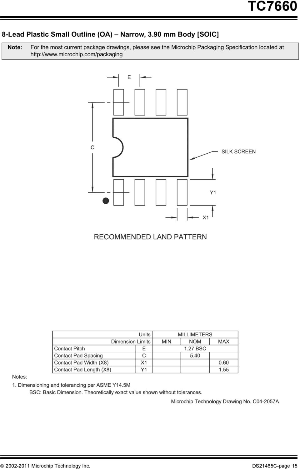
12 Note: For the most current package drawings, please see the Microchip Packaging Specification located at DSC-page - Microchip Technology Inc.

13 Note: For the most current package drawings, please see the Microchip Packaging Specification located at - Microchip Technology Inc. DSC-page

14 Note: For the most current package drawings, please see the Microchip Packaging Specification located at DSC-page - Microchip Technology Inc.

15 - Microchip Technology Inc. DSC-page
16 APPENDIX A: REVISION HISTORY Revision C (March ) The following is the list of modifications.. Updated Figure -.. Added Appendix A. Revision B (March ) Undocumented changes. Revision A (May ) Original release of this document. DSC-page - Microchip Technology Inc.
 Original release of this document.")
17 PRODUCT IDENTIFICATION SYSTEM To order or obtain information, e.g., on pricing or delivery, refer to the factory or the listed sales office. PART NO. X /XX Device Temperature Range Package Device: : DC-to-DC Voltage Converter Temperature Range: C = C to C E = - C to C I = - C to C (CERDIP only) M = - C to C (CERDIP only) Package: PA = Plastic DIP, ( mil body), -lead JA = Ceramic DIP, ( mil body), -lead OA = SOIC (Narrow), -lead OA = SOIC (Narrow), -lead (Tape and Reel) Examples: a) COA: Commercial Temp., SOIC package. b) COA:Tape and Reel, Commercial Temp., SOIC package. c) CPA: Commercial Temp., PDIP package. d) EOA: Extended Temp., SOIC package. e) EOA:Tape and Reel, Extended Temp., SOIC package. f) EPA: Extended Temp., PDIP package. g) IJA: Industrial Temp., CERDIP package h) MJA: Military Temp., CERDIP package. - Microchip Technology Inc. DSC-page
 COA:Tape and Reel, Commercial Temp., SOIC package. c) CPA: Commercial Temp., PDIP package. d) EOA: Extended Temp., SOIC package. e) EOA:Tape and Reel, Extended Temp., SOIC package. f) EPA: Extended Temp.")
18 NOTES: DSC-page - Microchip Technology Inc.

19 Note the following details of the code protection feature on Microchip devices: Microchip products meet the specification contained in their particular Microchip Data Sheet. Microchip believes that its family of products is one of the most secure families of its kind on the market today, when used in the intended manner and under normal conditions. There are dishonest and possibly illegal methods used to breach the code protection feature. All of these methods, to our knowledge, require using the Microchip products in a manner outside the operating specifications contained in Microchip s Data Sheets. Most likely, the person doing so is engaged in theft of intellectual property. Microchip is willing to work with the customer who is concerned about the integrity of their code. Neither Microchip nor any other semiconductor manufacturer can guarantee the security of their code. Code protection does not mean that we are guaranteeing the product as unbreakable. Code protection is constantly evolving. We at Microchip are committed to continuously improving the code protection features of our products. Attempts to break Microchip s code protection feature may be a violation of the Digital Millennium Copyright Act. If such acts allow unauthorized access to your software or other copyrighted work, you may have a right to sue for relief under that Act. Information contained in this publication regarding device applications and the like is provided only for your convenience and may be superseded by updates. It is your responsibility to ensure that your application meets with your specifications. MICROCHIP MAKES NO REPRESENTATIONS OR WARRANTIES OF ANY KIND WHETHER EXPRESS OR IMPLIED, WRITTEN OR ORAL, STATUTORY OR OTHERWISE, RELATED TO THE INFORMATION, INCLUDING BUT NOT LIMITED TO ITS CONDITION, QUALITY, PERFORMANCE, MERCHANTABILITY OR FITNESS FOR PURPOSE. Microchip disclaims all liability arising from this information and its use. Use of Microchip devices in life support and/or safety applications is entirely at the buyer s risk, and the buyer agrees to defend, indemnify and hold harmless Microchip from any and all damages, claims, suits, or expenses resulting from such use. No licenses are conveyed, implicitly or otherwise, under any Microchip intellectual property rights. Trademarks The Microchip name and logo, the Microchip logo, dspic, KEELOQ, KEELOQ logo, MPLAB, PIC, PICmicro, PICSTART, PIC logo, rfpic and UNI/O are registered trademarks of Microchip Technology Incorporated in the U.S.A. and other countries. FilterLab, Hampshire, HI-TECH C, Linear Active Thermistor, MXDEV, MXLAB, SEEVAL and The Embedded Control Solutions Company are registered trademarks of Microchip Technology Incorporated in the U.S.A. Analog-for-the-Digital Age, Application Maestro, chipkit, chipkit logo, CodeGuard, dspicdem, dspicdem.net, dspicworks, dsspeak, ECAN, ECONOMONITOR, FanSense, HI-TIDE, In-Circuit Serial Programming, ICSP, Mindi, MiWi, MPASM, MPLAB Certified logo, MPLIB, MPLINK, mtouch, Omniscient Code Generation, PICC, PICC-, PICDEM, PICDEM.net, PICkit, PICtail, REAL ICE, rflab, Select Mode, Total Endurance, TSHARC, UniWinDriver, WiperLock and ZENA are trademarks of Microchip Technology Incorporated in the U.S.A. and other countries. SQTP is a service mark of Microchip Technology Incorporated in the U.S.A. All other trademarks mentioned herein are property of their respective companies. -, Microchip Technology Incorporated, Printed in the U.S.A., All Rights Reserved. Printed on recycled paper. QUALITY MANAGEMENT SYSTEM CERTIFIED BY DNV == ISO/TS 99 == ISBN: Microchip received ISO/TS-99:9 certification for its worldwide headquarters, design and wafer fabrication facilities in Chandler and Tempe, Arizona; Gresham, Oregon and design centers in California and India. The Company s quality system processes and procedures are for its PIC MCUs and dspic DSCs, KEELOQ code hopping devices, Serial EEPROMs, microperipherals, nonvolatile memory and analog products. In addition, Microchip s quality system for the design and manufacture of development systems is ISO 9: certified. - Microchip Technology Inc. DSC-page 9

20 Worldwide Sales and Service AMERICAS Corporate Office West Chandler Blvd. Chandler, AZ -99 Tel: -9- Fax: -9- Technical Support: support Web Address: Atlanta Duluth, GA Tel: -9-9 Fax: -9- Boston Westborough, MA Tel: -- Fax: -- Chicago Itasca, IL Tel: -- Fax: -- Cleveland Independence, OH Tel: -- Fax: -- Dallas Addison, TX Tel: 9-- Fax: 9--9 Detroit Farmington Hills, MI Tel: -- Fax: -- Indianapolis Noblesville, IN Tel: -- Fax: -- Los Angeles Mission Viejo, CA Tel: Fax: Santa Clara Santa Clara, CA Tel: -9- Fax: -9- Toronto Mississauga, Ontario, Canada Tel: Fax: 9--9 ASIA/PACIFIC Asia Pacific Office Suites -, th Floor Tower, The Gateway Harbour City, Kowloon Hong Kong Tel: -- Fax: -- Australia - Sydney Tel: --9- Fax: --9- China - Beijing Tel: --9- Fax: --- China - Chengdu Tel: --- Fax: ---9 China - Chongqing Tel: Fax: China - Hangzhou Tel: --9- Fax: China - Hong Kong SAR Tel: -- Fax: -- China - Nanjing Tel: --- Fax: --- China - Qingdao Tel: --- Fax: --- China - Shanghai Tel: --- Fax: --- China - Shenyang Tel: ---9 Fax: ---9 China - Shenzhen Tel: --- Fax: --- China - Wuhan Tel: --9- Fax: --9- China - Xian Tel: -9-- Fax: -9-- China - Xiamen Tel: -9- Fax: -9- ASIA/PACIFIC India - Bangalore Tel: Fax: India - New Delhi Tel: 9--- Fax: 9--- India - Pune Tel: 9--- Fax: 9--- Japan - Osaka Tel: --- Fax: ---9 Japan - Yokohama Tel: --- Fax: --- Korea - Daegu Tel: --- Fax: --- Korea - Seoul Tel: --- Fax: ---9 or ---9 Malaysia - Kuala Lumpur Tel: ---9 Fax: Malaysia - Penang Tel: --- Fax: --- Philippines - Manila Tel: ---9 Fax: Singapore Tel: -- Fax: -- Taiwan - Hsin Chu Tel: --- Fax: ---9 Taiwan - Kaohsiung Tel: --- Fax: ---9 Taiwan - Taipei Tel: --- Fax: --- Thailand - Bangkok Tel: --9- Fax: --9- EUROPE Austria - Wels Tel: ---9 Fax: ---9 Denmark - Copenhagen Tel: -- Fax: --9 France - Paris Tel: Fax: Germany - Munich Tel: Fax: Italy - Milan Tel: 9-- Fax: 9-- Netherlands - Drunen Tel: Fax: --9 Spain - Madrid Tel: Fax: UK - Wokingham Tel: Fax: --9- China - Zhuhai Tel: -- Fax: --9 /9/ DSC-page - Microchip Technology Inc.

AN1286. Water-Resistant Capacitive Sensing INTRODUCTION THEORY OF OPERATION. Sensing Steps. Sensing Steps Description DESIGN
 Water-Resistant Capacitive Sensing AN1286 Author: INTRODUCTION Thomas Perme Steven Lin Microchip Technology Inc. This application note describes a new hardware sensing method which is resilient to water
TB3016. Using the PIC MCU CTMU for Temperature Measurement IMPLEMENTATION BASIC PRINCIPLE MEASUREMENT CIRCUIT
 Using the PIC MCU CTMU for Temperature Measurement Author: Padmaraja Yedamale Microchip Technology Inc. The Charge Time Measurement Unit (CTMU), introduced on the latest generation of PIC24F and PIC18F
Recommended Usage of Microchip 23X256/23X640 SPI Serial SRAM Devices RECOMMENDED CONNECTIONS FOR 23X256,23X640 SERIES DEVICES VCC 23X256/ HOLD.
 Recommended Usage of Microchip 23X256/23X640 SPI Serial SRAM Devices Author: INTRODUCTION Martin Bowman Microchip Technology Inc. This document details recommended usage of the Microchip 23X256 and 23X640
TC1047/TC1047A. Precision Temperature-to-Voltage Converter. General Description. Applications. Block Diagram. Features.
 Precision Temperature-to-Voltage Converter Features Supply Voltage Range: - TC147: 2.7V to 4.4V - TC147A: 2.V to.v Wide Temperature Measurement Range: - -4 o C to +12 o C High Temperature Converter Accuracy:
AN1303. Software Real-Time Clock and Calendar Using PIC16F1827 DATA INTERFACE INTRODUCTION IMPLEMENTATION INTERNAL REGISTER MAP
 Software Real-Time Clock and Calendar Using PIC16F1827 Author: INTRODUCTION Cristian Toma Microchip Technology Inc. This application note describes the implementation of software Real-Time Clock and Calendar
Installing and Licensing MPLAB XC C Compilers
 Installing and Licensing MPLAB XC C Compilers DS50002059G Note the following details of the code protection feature on Microchip devices: Microchip products meet the specification contained in their particular
Universal Programming Module 2
 Universal Programming Module OVERVIEW The Universal Programming Module (UPM) is a handy, low-cost board that supports the programming of Microchip devices using MPLAB in-circuit emulators and debuggers.
AN1325. mtouch Metal Over Cap Technology THEORY OF OPERATION INTRODUCTION CROSS SECTION OF METAL OVER CAPACITIVE (UNPRESSED)
") mtouch Metal Over Cap Technology AN1325 Authors: INTRODUCTION Keith Curtis Dieter Peter Microchip Technology Inc. As a user interface, capacitive touch has several advantages: it is low power, low cost,
mtouch Metal Over Cap Technology AN1325 Authors: INTRODUCTION Keith Curtis Dieter Peter Microchip Technology Inc. As a user interface, capacitive touch has several advantages: it is low power, low cost,
AN687. Precision Temperature-Sensing With RTD Circuits RTD OVERVIEW INTRODUCTION EQUATION 1:
 Precision Temperature-Sensing With RTD Circuits Author: INTRODUCTION Bonnie C. Baker Microchip Technology Inc. The most widely measured phenomena in the process control environment is temperature. Common
AN1142. USB Mass Storage Class on an Embedded Host INTRODUCTION. USB Mass Storage Class. Overview
 USB Mass Storage Class on an Embedded Host Author: INTRODUCTION With the introduction of Microchip's microcontrollers with the USB OTG peripheral, microcontroller applications can easily support USB Embedded
AN1470. Manchester Decoder Using the CLC and NCO ABSTRACT INTRODUCTION MANCHESTER ENCODED DATA (AS PER G.E. THOMAS)
") Manchester Decoder Using the CLC and NCO Authors: ABSTRACT A Manchester decoder can be built using Microchip s award winning CLC (Configurable Logic Cell) blocks and NCO (Numerically Controlled Oscillator)
Manchester Decoder Using the CLC and NCO Authors: ABSTRACT A Manchester decoder can be built using Microchip s award winning CLC (Configurable Logic Cell) blocks and NCO (Numerically Controlled Oscillator)
AN1199. 1-Wire Communication with PIC Microcontroller INTRODUCTION. OVERVIEW OF THE 1-Wire BUS. 1-Wire Protocol. Prerequisites
 1-Wire Communication with PIC Microcontroller Author: INTRODUCTION This application note introduces the user to the 1-Wire communication protocol and describes how a 1-Wire device can be interfaced to
AN1332. Current Sensing Circuit Concepts and Fundamentals CURRENT SENSING RESISTOR INTRODUCTION. Description. Microchip Technology Inc.
 Current Sensing Circuit Concepts and Fundamentals Author: INTRODUCTION Yang Zhen Microchip Technology Inc. Current sensing is a fundamental requirement in a wide range of electronic applications. Typical
Uninstalling Incorrect USB Device Drivers
 DEVELOPMENT SYSTEMS Uninstalling Incorrect USB Device Drivers RECOMMENDED UNINSTALL METHODS When using the Microchip development tools listed below, trouble may be experienced as a result of incorrect
Features, Value and Benefits of Digital Control for Power Supplies
 Author: INTRODUCTION Sagar Khare Microchip Technology Inc. Control of Switch Mode Power Supplies (SMPSs) has traditionally been a purely analog domain. The advent of low-cost, high-performance Digital
AN1156. Battery Fuel Measurement Using Delta-Sigma ADC Devices INTRODUCTION REVIEW OF BATTERY CHARGING AND DISCHARGING CHARACTERISTICS
 Battery Fuel Measurement Using Delta-Sigma ADC Devices Author: INTRODUCTION Youbok Lee, Ph.D. Microchip Technology Inc. The battery fuel status indicator is a common feature of the battery-supported handheld
AN1492. Microchip Capacitive Proximity Design Guide INTRODUCTION CAPACITIVE SENSING BASICS SENSING
 Microchip Capacitive Proximity Design Guide Author: INTRODUCTION Xiang Gao Microchip Technology Inc. Proximity detection provides a new way for users to interact with electronic devices without having
AN1353. Op Amp Rectifiers, Peak Detectors and Clamps INTRODUCTION BASIC RECTIFIERS. Choosing the Components. Positive Half-Wave Rectifier.
 Op Amp Rectifiers, Peak Detectors and Clamps Author: Dragos Ducu, Microchip Technology Inc. INTRODUCTION This application note covers a wide range of applications, such as halfwave rectifiers, fullwave
AN1275. KEELOQ with Advanced Encryption Standard (AES) Receiver/Decoder KEY FEATURES OVERVIEW. Microchip Technology Inc.
 Receiver/Decoder KEY FEATURES OVERVIEW. Microchip Technology Inc.") KEELOQ with Advanced Encryption Standard (AES) Receiver/Decoder Author: OVERVIEW Enrique Aleman Microchip Technology Inc. This application note describes a KEELOQ with AES code hopping decoder implemented
KEELOQ with Advanced Encryption Standard (AES) Receiver/Decoder Author: OVERVIEW Enrique Aleman Microchip Technology Inc. This application note describes a KEELOQ with AES code hopping decoder implemented
AN1857. RGBW Color Mixing DALI Control Gear. COLOR MIXING USING RED, GREEN, BLUE AND WHITE LEDs INTRODUCTION HARDWARE
 RGBW Color Mixing DALI Control Gear AN1857 Author: INTRODUCTION Mihai Cuciuc Microchip Technology Inc. This application note provides an example of obtaining custom colors by combining the spectra of the
AN1543. Using MRF24W with PIC32 Internal Program Flash Memory For EZ_CONFIG_STORE ALTERNATIVE LOW-COST SOLUTIONS OVERVIEW SCOPE
 Using MRF24W with PIC32 Internal Program Flash Memory For EZ_CONFIG_STORE Author: OVERVIEW This application note describes the EZ_CONFIG_STORE feature used in the Wi-Fi G Demo Board and TCPIP-WiFi EZConfig
AN905. Brushed DC Motor Fundamentals INTRODUCTION PRINCIPLES OF OPERATION. Stator. Rotor SIMPLE TWO-POLE BRUSHED DC MOTOR. Microchip Technology Inc.
 Brushed DC Motor Fundamentals AN905 Author: Reston Condit Microchip Technology Inc. INTRODUCTION Brushed DC motors are widely used in applications ranging from toys to push-button adjustable car seats.
Touch Through Metal. mtouch Metal Over Capacitive Technology Part 1
 Touch Through Metal mtouch Metal Over Capacitive Technology Part 1 2010 Microchip Technology Incorporated. All Rights Reserved. Touch Through Metal Slide 1 Hello and welcome to Microchip s Touch Through
Designing A Li-Ion Battery Charger and Load Sharing System With Microchip s Stand-Alone Li-Ion Battery Charge Management Controller
 Designing A Li-Ion Battery Charger and Load Sharing System With Microchip s Stand-Alone Li-Ion Battery Charge Management Controller Author: INTRODUCTION Brian Chu Microchip Technology Inc. Batteries often
MCP73X23 Lithium Iron Phosphate (LiFePO 4 ) Battery Charger Evaluation Board User s Guide
 Battery Charger Evaluation Board User s Guide") MCP73X23 Lithium Iron Phosphate (LiFePO 4 ) Battery Charger Evaluation Board User s Guide 2009 Microchip Technology Inc. DS51850A Note the following details of the code protection feature on Microchip
MCP73X23 Lithium Iron Phosphate (LiFePO 4 ) Battery Charger Evaluation Board User s Guide 2009 Microchip Technology Inc. DS51850A Note the following details of the code protection feature on Microchip
HT7660. CMOS Switched-Capacitor Voltage Converter. Features. Applications. General Description. Block Diagram
 CMOS Switched-Capacitor Voltage Converter Features Simple conversion of V DD to V DD Cascade connection (two devices are connected, V OUT = 2 V DD ) Boost pin for higher switching frequency Easy to use
MCP1701A. 2 µa Low-Dropout Positive Voltage Regulator. Features. General Description. Applications. Package Types
 2 µa Low-Dropout Positive Voltage Regulator Features 2.0 µa Typical Quiescent Current Input Operating Voltage Range up to 10.0V Low-Dropout Voltage (LDO): - 120 mv (typical) @ 100 ma - 380 mv (typical)
PDIP, MSOP, SOIC, TSSOP
 2.7V Dual Channel 12-Bit A/D Converter with SPI Serial Interface Features 12-bit resolution ±1 LSB maximum DNL ±1 LSB maximum INL (MCP3202-B) ±2 LSB maximum INL (MCP3202-C) Analog inputs programmable as
Section 15. Input Capture
 Section 15. Input Capture HIGHLIGHTS This section of the manual contains the following topics: 15.1 Introduction...15-2 15.2 Input Capture Registers...15-4 15.3 Timer Selection...15-8 15.4 Input Capture
Timers: Timer0 Tutorial (Part 1)
") Timers: Timer0 Tutorial (Part 1) 2007 Microchip Technology Inc. DS51682A Note the following details of the code protection feature on Microchip devices: Microchip products meet the specification contained
Timers: Timer0 Tutorial (Part 1) 2007 Microchip Technology Inc. DS51682A Note the following details of the code protection feature on Microchip devices: Microchip products meet the specification contained
AN1066. Microchip MiWi Wireless Networking Protocol Stack INTRODUCTION CONSIDERATIONS TERMINOLOGY FEATURES
 Microchip MiWi Wireless Networking Protocol Stack Author: INTRODUCTION Implementing applications with wireless networking is now common. From consumer devices to industrial applications, there is a growing
MCP3021. Low Power 10-Bit A/D Converter With I 2 C Interface. Description. Features. Applications. Functional Block Diagram.
 MCP321 Low Power 1-Bit A/D Converter With I 2 C Interface Features 1-bit resolution ±1 LSB DNL, ±1 LSB INL max. 25 µa max conversion current 5 na typical standby current, 1 µa max. I 2 C compatible serial
TCM809/TCM810. 3-Pin Microcontroller Reset Monitors. General Description. Features. Applications. Pin Configurations. Typical Application Circuit
 3-Pin Microcontroller Reset Monitors Features Precision Monitor for 2.5V, 3.V, 3.3V, 5.V Nominal System Voltage Supplies 14 msec Minimum RESET Time-Out Period RESET Output to = 1.V (TCM89) Low Supply Current,
MCP14A0151/2. 1.5A MOSFET Driver with Low Threshold Input And Enable. Features. General Description. Applications. Package Types
 1.5A MOSFET Driver with Low Threshold Input And Enable Features High Peak Output Current: 1.5A (typical) Wide Input Supply Voltage Operating Range: - 4.5V to 18V Low Shoot-Through/Cross-Conduction Current
MCP73811/2. Simple, Miniature Single-Cell, Fully Integrated Li-Ion / Li-Polymer Charge Management Controllers. Description. Features.
 Simple, Miniature Single-Cell, Fully Integrated Li-Ion / Li-Polymer Charge Management Controllers Features Complete Linear Charge Management Controller - Integrated Pass Transistor - Integrated Current
MCP2200 USB to RS-232 Demo Board User s Guide
 MCP2200 USB to RS-232 Demo Board User s Guide DS51901A Note the following details of the code protection feature on Microchip devices: Microchip products meet the specification contained in their particular
AN1465. Digitally Addressable Lighting Interface (DALI) Communication TERMINOLOGY PHYSICAL LAYER DALI FREE-FORM LAYOUT. Topology FIGURE 1:
 Communication TERMINOLOGY PHYSICAL LAYER DALI FREE-FORM LAYOUT. Topology FIGURE 1:") Digitally Addressable Lighting Interface (DALI) Communication Author: Shaima Husain Microchip Technology Inc. The Digitally Addressable Lighting Interface (DALI) has emerged as a standard in Europe to
Digitally Addressable Lighting Interface (DALI) Communication Author: Shaima Husain Microchip Technology Inc. The Digitally Addressable Lighting Interface (DALI) has emerged as a standard in Europe to
ICL232. +5V Powered, Dual RS-232 Transmitter/Receiver. Description. Features. Ordering Information. Applications. Functional Diagram.
 ICL August V Powered, Dual RS Transmitter/Receiver Features Meets All RSC and V. Specifications Requires Only Single V Power Supply Onboard Voltage Doubler/Inverter Low Power Consumption Drivers ±V Output
TC4423A/TC4424A/TC4425A
 3A Dual High-Speed Power MOSFET Drivers Features High Peak Output Current: 4.5A (typical) Wide Input Supply Voltage Operating Range: - 4.5V to 18V High Capacitive Load Drive Capability: - 18 pf in 12 ns
AN1265. KEELOQ with AES Microcontroller-Based Code Hopping Encoder INTRODUCTION DUAL ENCODER OPERATION BACKGROUND FUNCTIONAL INPUTS AND
 KEELOQ with AES Microcontroller-Based Code Hopping Encoder Authors: INTRODUCTION This application note describes the design of a microcontroller-based KEELOQ Hopping Encoder using the AES encryption algorithm.
Resistive Temperature Detector (RTD) Reference Design
 Reference Design") Resistive Temperature Detector (RTD) Reference Design DS51891A Note the following details of the code protection feature on Microchip devices: Microchip products meet the specification contained in their
Resistive Temperature Detector (RTD) Reference Design DS51891A Note the following details of the code protection feature on Microchip devices: Microchip products meet the specification contained in their
28-PIN DEMO BOARD USER S GUIDE
 28-PIN DEMO BOARD USER S GUIDE 2006-2015 Microchip Technology Inc. DS40001301B Note the following details of the code protection feature on Microchip devices: Microchip products meet the specification
TC4421/TC4422. Functional Block Diagram. TC4421 Inverting. TC4422 Non-Inverting V DD. 300 mv Output. Input 4.7V. GND Effective. Input.
 9A High-Speed MOSFET Drivers Features High Peak Output Current: 9A Wide Input Supply Voltage Operating Range: - 4.5V to 18V High Continuous Output Current: 2A Max Fast Rise and Fall Times: - 3 ns with
MCP3004/3008. 2.7V 4-Channel/8-Channel 10-Bit A/D Converters with SPI Serial Interface. Features. Description. Applications.
 2.7V 4-Channel/8-Channel 10-Bit A/D Converters with SPI Serial Interface Features 10-bit resolution ± 1 LSB max DNL ± 1 LSB max INL 4 (MCP3004) or 8 (MCP3008) input channels Analog inputs programmable
ICL7660, ICL7660A. CMOS Voltage Converters. Features. Applications. Pinouts FN3072.7. Data Sheet October 10, 2005
 ICL, ICLA Data Sheet October, FN. CMOS Voltage Converters The Intersil ICL and ICLA are monolithic CMOS power supply circuits which offer unique performance advantages over previously available devices.
1.5A Dual MOSFET Driver with Low Threshold Input And Enable MCP14A0155 8 7 OUT A OUT A OUT A IN A GND IN B
 1.5A Dual MOSFET Driver with Low Threshold Input And Enable Features High Peak Output Current: 1.5A (typical) Wide Input Supply Voltage Operating Range: - 4.5V to 18V Low Shoot-Through/Cross-Conduction
Section 5. Flash Programming
 Section 5. Flash Programming HIGHLIGHTS This section of the manual contains the following topics: 5.1 Introduction...5-2 5.2 Control Registers... 5-3 5.3 Run-Time Self-Programming (RTSP) Operation... 5-10
PIC18F26K20/46K20 Rev. B2/B3/B5/B6 Silicon Errata and Data Sheet Clarification
 PIC18F26K20/46K20 Rev. B2/B3/B5/B6 Silicon Errata and Data Sheet Clarification The PIC18F26K20/46K20 family devices that you have received conform functionally to the current Device Data Sheet (DS41303G),
Serial EEPROM Powered for Automotive
 Automotive Memory Products Serial EEPROM Powered for Automotive www.microchip.com/memory Microchip Serial Memory Products Microchip Technology has developed industry-leading processes for each step in
ICL7660, ICL7660A. CMOS Voltage Converters. Features. itle L76, L76 A) bjec. ltag. nver s) utho ) eyw s tersi. Applications.
 bjec. ltag. nver s) utho ) eyw s tersi. Applications.") TM ICL, ICLA Data Sheet April 999 File Number. itle L, L A) bjec MO ltag nver s) utho ) eyw s tersi rpor on, arge mp, ltage nvert ltage uble ltage erte X, X, C, CMOS Voltage Converters The Intersil ICL
TM ICL, ICLA Data Sheet April 999 File Number. itle L, L A) bjec MO ltag nver s) utho ) eyw s tersi rpor on, arge mp, ltage nvert ltage uble ltage erte X, X, C, CMOS Voltage Converters The Intersil ICL
CMOS Switched-Capacitor Voltage Converters ADM660/ADM8660
 CMOS Switched-Capacitor Voltage Converters ADM66/ADM866 FEATURES ADM66: Inverts or Doubles Input Supply Voltage ADM866: Inverts Input Supply Voltage ma Output Current Shutdown Function (ADM866) 2.2 F or
MCP3204/3208. 2.7V 4-Channel/8-Channel 12-Bit A/D Converters with SPI Serial Interface. Features. Description. Applications.
 2.7V 4-Channel/8-Channel 12-Bit A/D Converters with SPI Serial Interface Features 12-bit resolution ± 1 LSB max DNL ± 1 LSB max INL (MCP3204/3208-B) ± 2 LSB max INL (MCP3204/3208-C) 4 (MCP3204) or 8 (MCP3208)
AN1212. Using USB Keyboard with an Embedded Host INTRODUCTION. USB Keyboard Overview. USB Keyboard with an Embedded Host USB KEYBOARD OUTPUT REPORT
 Using USB Keyboard with an Embedded Host Author: INTRODUCTION Amardeep Gupta Microchip Technology Inc. Microcontroller applications can easily support USB embedded host functionality with the introduction
PIC32 Microcontroller Families
 32-bit Microcontrollers Winter 2009 PIC32 Microcontroller Families With USB, CAN and Ethernet www.microchip.com/pic32 Building on the heritage of Microchip Technology s world-leading 8- and 16-bit PIC
High-Speed, 5 V, 0.1 F CMOS RS-232 Driver/Receivers ADM202/ADM203
 a FEATURES kb Transmission Rate ADM: Small (. F) Charge Pump Capacitors ADM3: No External Capacitors Required Single V Power Supply Meets EIA-3-E and V. Specifications Two Drivers and Two Receivers On-Board
AN1256. Microchip s Power MOSFET Driver Simulation Models INTRODUCTION MODEL DESCRIPTION. Using The Power MOSFET Simulation Models
 Microchip s Power MOSFET Driver Simulation Models Author: INTRODUCTION Cliff Ellison (Microchip Technology Inc.) Ron Wunderlich (Innovative Ideas and Design) The simulation models for Microchip s power
AN1307 FULL STEP MODE PHASE VOLTAGE AND PHASE CURRENT MICROSTEPPING WITH 1/4 STEP SIZE
 Stepper Motor Control with dspic DSCs AN1307 Author: INTRODUCTION Sorin Manea Microchip Technology Inc. This application note describes how to drive a stepper motor with a dspic33f motor control family
MPLAB Code Configurator User s Guide
 MPLAB Code Configurator User s Guide 2013-2014 Microchip Technology Inc. DS40001725B MPLAB CODE CONFIGURATOR USER S GUIDE Note the following details of the code protection feature on Microchip devices:
WORKSHOP-IN-A-BOX 2: LOW POWER SOLUTIONS DEMONSTRATION BOARD
 WORKSHOP-IN-A-BOX 2: LOW POWER SOLUTIONS DEMONSTRATION BOARD 2004 Microchip Technology Inc. DS51512A Note the following details of the code protection feature on Microchip devices: Microchip products meet
TRIPLE PLL FIELD PROG. SPREAD SPECTRUM CLOCK SYNTHESIZER. Features
 DATASHEET ICS280 Description The ICS280 field programmable spread spectrum clock synthesizer generates up to four high-quality, high-frequency clock outputs including multiple reference clocks from a low-frequency
MPLAB XC8 GETTING STARTED GUIDE. MPLAB XC8 Getting Started Guide
 MPLAB XC8 GETTING STARTED GUIDE MPLAB XC8 Getting Started Guide This document provides a starting point for programmers who are just starting out with the MPLAB XC8 C Compiler, particularly those who are
Peripheral Brief: Programmable Switch Mode Controller (PSMC) 1, 2, 4, 8 PSMCXTMR CLR PSMCXPR = Period. Event PSMCXPRS. Rising.
 1, 2, 4, 8 PSMCXTMR CLR PSMCXPR = Period. Event PSMCXPRS. Rising.") Peripheral Brief: Programmable Switch Mode Controller (PSMC) Author: INTRODUCTION John Mouton Microchip Technology Inc. This peripheral brief reviews the basic functionality of the Programmable Switch
Peripheral Brief: Programmable Switch Mode Controller (PSMC) Author: INTRODUCTION John Mouton Microchip Technology Inc. This peripheral brief reviews the basic functionality of the Programmable Switch
Description. Table 1. Device summary. Order code Temperature range Package Packaging Marking
 14-stage ripple carry binary counter/divider and oscillator Applications Automotive Industrial Computer Consumer Description Datasheet - production data Features Medium speed operation Common reset Fully
Selecting the MCU Memory Technology That s Right for You
 ROM Microcontrollers Selecting the MCU Memory Technology That s Right for You Seamless Migration From To ROM www.microchip.com Many Applications Require Flexible Solutions Selecting only one microcontroller
AN1426. Design Tips for the MCP3911 INTRODUCTION. Addressable Devices on Single SPI Bus. Addressable SPI for Poly-phase Meter Designs.
 Design Tips for the MCP3911 AN1426 Author: Craig King Microchip Technology Inc. Here, pushing the limits of the analog-to-digital conversion will be the focus, showing the true performance limits of the
TC4420/TC4429. 6A High-Speed MOSFET Drivers. General Description. Features. Applications. Package Types (1)
") 6A High-Speed MOSFET Drivers Features atch-up Protected: Will Withstand >1.5A Reverse Output Current ogic Input Will Withstand Negative Swing Up To 5V ESD Protected: 4 kv Matched Rise and Fall Times: -
6A High-Speed MOSFET Drivers Features atch-up Protected: Will Withstand >1.5A Reverse Output Current ogic Input Will Withstand Negative Swing Up To 5V ESD Protected: 4 kv Matched Rise and Fall Times: -
ICS514 LOCO PLL CLOCK GENERATOR. Description. Features. Block Diagram DATASHEET
 DATASHEET ICS514 Description The ICS514 LOCO TM is the most cost effective way to generate a high-quality, high-frequency clock output from a 14.31818 MHz crystal or clock input. The name LOCO stands for
5A LOW DROPOUT LINEAR REGULATOR General Description. Features. Applications
 General Description The is a series of low dropout positive voltage regulators with a maximum dropout of.5v at 5A of load current. The series features on-chip thermal limiting which provides protection
TCM680. +5V To ±10V Voltage Converter. General Description. Features. Applications. Package Type. Typical Operating Circuit
 M 5V To ±10V Voltage Converter TCM680 Features 99% Voltage Conversion Efficiency 85% Power Conversion Efficiency Input Voltage Range: 2.0V to 5.5V Only 4 External Capacitors Required 8Pin SOIC Package
High-Speed CAN Transceiver. Thermal Shutdown. Dominant Detect. Driver. Control. Power-On Reset 0.5 VDD. Receiver
 High-Speed CAN Transceiver MCP2551 Features Supports 1 Mb/s operation Implements ISO-11898 standard physical layer requirements Suitable for 12V and 24V systems Externally-controlled slope for reduced
Features INVERTING. 0.6mA NONINVERTING INVERTING. 0.6mA NONINVERTING
 MIC442/442/4428 Dual 1.A-Peak Low-Side MOSFET Driver General Description The MIC442/442/4428 family are highly-reliable dual lowside MOSFET drivers fabricated on a BiCMOS/DMOS process for low power consumption
HCC4541B HCF4541B PROGRAMMABLE TIMER
 HCC4541B HCF4541B PROGRAMMABLE TIMER 16 STAGE BINARI COUNTER LOW SYMMETRICAL OUTPUT RESISTANCE, TYPICALLY 100 OHM AT DD = 15 OSCILLATOR FREQUENCY RANGE : DC TO 100kHz AUTO OR MASTER RESET DISABLES OSCIL-
AN645. PIC16C57 Based Code Hopping Security System PINOUT OVERVIEW FEATURES BLOCK DIAGRAM RECOMMENDED READING
 PI657 Based ode Hopping Security System Author: OVERVIEW This document describes a PI657 based code hopping automotive security system. The security system implements all the basic features found on security
dspic30f3012/3013 dspic30f3012/3013 Rev. B0 Silicon Errata dspic30f3012/3013 (Rev. B0) Silicon Errata Silicon Errata Summary
 Silicon Errata Silicon Errata Summary") dspic30f3012/3013 Rev. B0 Silicon Errata dspic30f3012/3013 (Rev. B0) Silicon Errata The dspic30f3012/3013 (Rev. B0) samples you have received were found to conform to the specifications and functionality
dspic30f3012/3013 Rev. B0 Silicon Errata dspic30f3012/3013 (Rev. B0) Silicon Errata The dspic30f3012/3013 (Rev. B0) samples you have received were found to conform to the specifications and functionality
MCP2515 CAN Bus Monitor Demo Board User s Guide
 MCP2515 CAN Bus Monitor Demo Board User s Guide 2008 Microchip Technology Inc. DS51757A Note the following details of the code protection feature on Microchip devices: Microchip products meet the specification
Analog-to-Digital Converters
 Analog-to-Digital Converters In this presentation we will look at the Analog-to-Digital Converter Peripherals with Microchip s midrange PICmicro Microcontrollers series. 1 Analog-to-Digital Converters
1 TO 4 CLOCK BUFFER ICS551. Description. Features. Block Diagram DATASHEET
 DATASHEET 1 TO 4 CLOCK BUFFER ICS551 Description The ICS551 is a low cost, high-speed single input to four output clock buffer. Part of IDT s ClockBlocks TM family, this is our lowest cost, small clock
CAT661. High Frequency 100 ma CMOS Charge Pump, Inverter/Doubler
 CAT High Frequency ma CMOS Charge Pump, Inverter/Doubler Description The CAT is a charge pump voltage converter. It can invert a positive input voltage to a negative output. Only two external capacitors
HCF4001B QUAD 2-INPUT NOR GATE
 QUAD 2-INPUT NOR GATE PROPAGATION DELAY TIME: t PD = 50ns (TYP.) at V DD = 10V C L = 50pF BUFFERED INPUTS AND OUTPUTS STANDARDIZED SYMMETRICAL OUTPUT CHARACTERISTICS QUIESCENT CURRENT SPECIFIED UP TO 20V
AN1861. Bluetooth Smart Communication Using Microchip RN4020 Module and 16-bit PIC Microcontroller BLUETOOTH SMART COMMUNICATION INTRODUCTION
 Bluetooth Smart Communication Using Microchip RN4020 Module and 16-bit PIC Microcontroller Author: Venkatesh Bengeri and Pradeep Shamanna INTRODUCTION Most of the embedded applications require real-time
Integrated Development Environment
 Development Tools Integrated Development Environment Transforming Ideas Into Realities The typical product development life cycle is comprised of smaller cycles each representing an iterative process toward
DG2302. High-Speed, Low r ON, SPST Analog Switch. Vishay Siliconix. (1-Bit Bus Switch with Level-Shifter) RoHS* COMPLIANT DESCRIPTION FEATURES
 RoHS* COMPLIANT DESCRIPTION FEATURES") High-Speed, Low r ON, SPST Analog Switch (1-Bit Bus Switch with Level-Shifter) DG2302 DESCRIPTION The DG2302 is a high-speed, 1-bit, low power, TTLcompatible bus switch. Using sub-micron CMOS technology,
High-Speed, Low r ON, SPST Analog Switch (1-Bit Bus Switch with Level-Shifter) DG2302 DESCRIPTION The DG2302 is a high-speed, 1-bit, low power, TTLcompatible bus switch. Using sub-micron CMOS technology,
HCF4010B HEX BUFFER/CONVERTER (NON INVERTING)
") HEX BUFFER/CONVERTER (NON INVERTING) PROPAGATION DELAY TIME: t PD = 50ns (Typ.) at V DD = 10V C L = 50pF HIGH TO LOW LEVEL LOGIC CONVERSION MULTIPLEXER: 1 TO 6 OR 6 TO 1 HIGH "SINK" AND "SOURCE" CURRENT
HEX BUFFER/CONVERTER (NON INVERTING) PROPAGATION DELAY TIME: t PD = 50ns (Typ.) at V DD = 10V C L = 50pF HIGH TO LOW LEVEL LOGIC CONVERSION MULTIPLEXER: 1 TO 6 OR 6 TO 1 HIGH "SINK" AND "SOURCE" CURRENT
MC33079. Low noise quad operational amplifier. Features. Description
 Low noise quad operational amplifier Datasheet production data Features Low voltage noise: 4.5 nv/ Hz High gain bandwidth product: 15 MHz High slew rate: 7 V/µs Low distortion: 0.002% Large output voltage
High-Speed, Low r ON, SPST Analog Switch (1-Bit Bus Switch)
") High-Speed, Low r ON, SPST Analog Switch (1-Bit Bus Switch) DG2301 ishay Siliconix DESCRIPTION The DG2301 is a high-speed, 1-bit, low power, TTLcompatible bus switch. Using sub-micron CMOS technology,
High-Speed, Low r ON, SPST Analog Switch (1-Bit Bus Switch) DG2301 ishay Siliconix DESCRIPTION The DG2301 is a high-speed, 1-bit, low power, TTLcompatible bus switch. Using sub-micron CMOS technology,
PAM2804. Pin Assignments. Description. Applications. Features. Typical Applications Circuit 1A STEP-DOWN CONSTANT CURRENT, HIGH EFFICIENCY LED DRIVER
 1A STEP-DOWN CONSTANT CURRENT, HIGH EFFICIENCY LED DRIER Description Pin Assignments The is a step-down constant current LED driver. When the input voltage is down to lower than LED forward voltage, then
AN1767. Solutions for Radio Frequency Electromagnetic Interference in Amplifier Circuits WHAT IS ELECTROMAGNETIC INTERFERENCE (EMI)
") Solutions for Radio Frequency Electromagnetic Interference in Amplifier Circuits Author: Dragos-George Ducu Microchip Technology Inc. WHAT IS ELECTROMAGNETIC INTERFERENCE (EMI) Nowadays, the number of
Solutions for Radio Frequency Electromagnetic Interference in Amplifier Circuits Author: Dragos-George Ducu Microchip Technology Inc. WHAT IS ELECTROMAGNETIC INTERFERENCE (EMI) Nowadays, the number of
SPREAD SPECTRUM CLOCK GENERATOR. Features
 DATASHEET ICS7152 Description The ICS7152-01, -02, -11, and -12 are clock generators for EMI (Electro Magnetic Interference) reduction (see below for frequency ranges and multiplier ratios). Spectral peaks
ICS650-44 SPREAD SPECTRUM CLOCK SYNTHESIZER. Description. Features. Block Diagram DATASHEET
 DATASHEET ICS650-44 Description The ICS650-44 is a spread spectrum clock synthesizer intended for video projector and digital TV applications. It generates three copies of an EMI optimized 50 MHz clock
AN884. Driving Capacitive Loads With Op Amps INTRODUCTION LINEAR RESPONSE. Simplified Op Amp AC Model. Overview. Purpose OP AMP MODEL EQUATION 1:
 Driving Capacitive Loads With Op Amps AN884 Author: INTRODUCTION Overview Operational amplifiers (op amps) that drive large capacitive loads may produce undesired results. This application note discusses
UA741. General-purpose single operational amplifier. Features. Applications. Description. N DIP8 (plastic package)
") General-purpose single operational amplifier Datasheet - production data N DIP8 (plastic package) D SO8 (plastic micropackage) Pin connections (top view) 1 - Offset null 1 2 - Inverting input 3 - Non-inverting
General-purpose single operational amplifier Datasheet - production data N DIP8 (plastic package) D SO8 (plastic micropackage) Pin connections (top view) 1 - Offset null 1 2 - Inverting input 3 - Non-inverting
AN1387. Using PIC32 MCUs to Develop Low-Cost Controllerless (LCC) Graphics Solutions INTRODUCTION. Basic Graphics Definitions
 Graphics Solutions INTRODUCTION. Basic Graphics Definitions") Using PIC32 MCUs to Develop Low-Cost Controllerless (LCC) Graphics Solutions Author: INTRODUCTION Adam Folts, Microchip Technology Inc. As the demand for Graphical Embedded Applications becomes more popular,
Using PIC32 MCUs to Develop Low-Cost Controllerless (LCC) Graphics Solutions Author: INTRODUCTION Adam Folts, Microchip Technology Inc. As the demand for Graphical Embedded Applications becomes more popular,
STCS1A. 1.5 A max constant current LED driver. Features. Applications. Description
 1.5 A max constant current LED driver Features Up to 40 V input voltage Less than 0.5 V voltage overhead Up to 1.5 A output current PWM dimming pin Shutdown pin LED disconnection diagnostic DFN8 (3 x 3
HCC/HCF4032B HCC/HCF4038B
 HCC/HCF4032B HCC/HCF4038B TRIPLE SERIAL ADDERS INERT INPUTS ON ALL ADDERS FOR SUM COMPLEMENTING APPLICATIONS FULLY STATIC OPERATION...DC TO 10MHz (typ.) @ DD = 10 BUFFERED INPUTS AND OUTPUTS SINGLE-PHASE
MIC4451/4452. General Description. Features. Applications. Functional Diagram V S. 12A-Peak Low-Side MOSFET Driver. Bipolar/CMOS/DMOS Process
 12A-Peak Low-Side MOSFET Driver Bipolar/CMOS/DMOS Process General Description MIC4451 and MIC4452 CMOS MOSFET drivers are robust, efficient, and easy to use. The MIC4451 is an inverting driver, while the
AN709. System Level Design Considerations When Using I 2 C TM Serial EEPROM Devices INTRODUCTION INSURING BUS-FREE DURING POWER-UP
 M AN709 System Level Design Considerations When Using I 2 C TM Serial EEPROM Devices Author: INTRODUCTION Rick Stoneking Developing systems that implement the I 2 C protocol for communicating with serial
Description SO-8. series. Furthermore, in the 8-pin configuration Very low-dropout voltage (0.2 V typ.)
") ery low-dropout voltage regulator with inhibit function TO-92 Bag TO-92 Tape and reel Ammopack 1 2 3 SO-8 Description Datasheet - production data The is a very low-dropout voltage regulator available in
ery low-dropout voltage regulator with inhibit function TO-92 Bag TO-92 Tape and reel Ammopack 1 2 3 SO-8 Description Datasheet - production data The is a very low-dropout voltage regulator available in
MC14008B. 4-Bit Full Adder
 4-Bit Full Adder The MC4008B 4bit full adder is constructed with MOS PChannel and NChannel enhancement mode devices in a single monolithic structure. This device consists of four full adders with fast
Obsolete Product(s) - Obsolete Product(s)
 - Obsolete Product(s)") SYNCHRONOUS PROGRAMMABLE 4-BIT BINARY COUNTER WITH ASYNCHRONOUS CLEAR INTERNAL LOOK-AHEAD FOR FAST COUNTING CARRY OUTPUT FOR CASCADING SYNCHRONOUSLY PROGRAMMABLE LOW-POWER TTL COMPATIBILITY STANDARDIZED
SYNCHRONOUS PROGRAMMABLE 4-BIT BINARY COUNTER WITH ASYNCHRONOUS CLEAR INTERNAL LOOK-AHEAD FOR FAST COUNTING CARRY OUTPUT FOR CASCADING SYNCHRONOUSLY PROGRAMMABLE LOW-POWER TTL COMPATIBILITY STANDARDIZED
LTC1390 8-Channel Analog Multiplexer with Serial Interface U DESCRIPTIO
 FEATRES -Wire Serial Digital Interface Data Retransmission Allows Series Connection with Serial A/D Converters Single V to ±V Supply Operation Analog Inputs May Extend to Supply Rails Low Charge Injection