DFM Flex - FlexRigid
|
|
|
- Caitlin Hutchinson
- 8 years ago
- Views:
Transcription
1 DFM Flex - FlexRigid
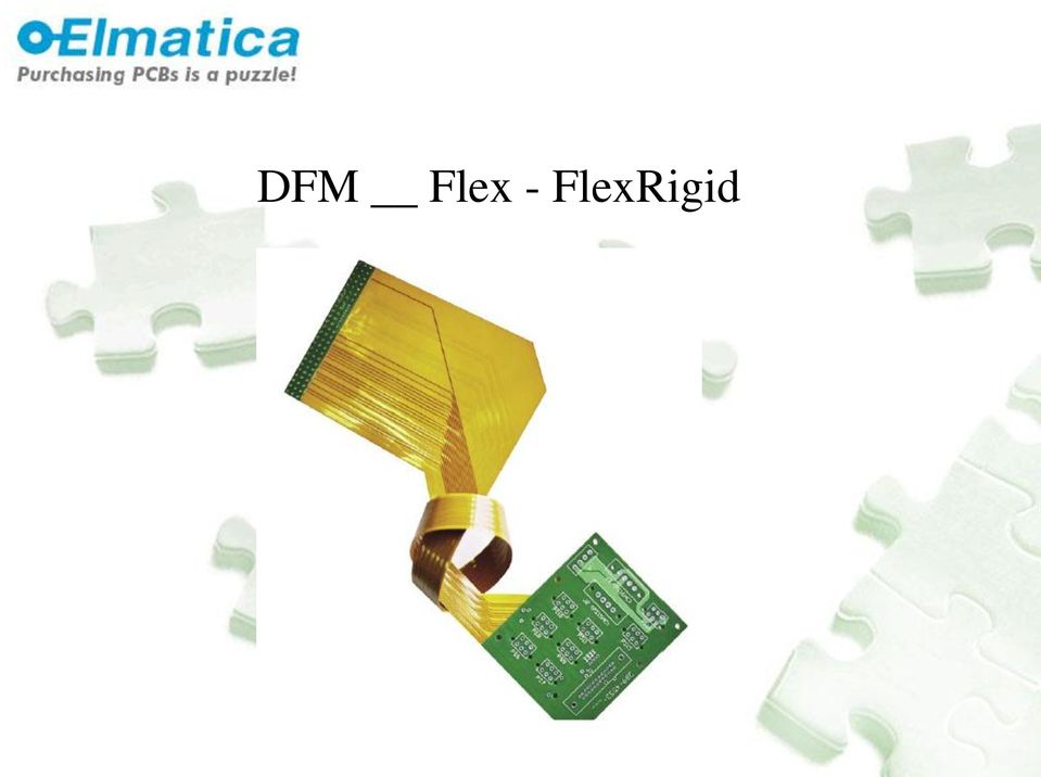
2 Wire harnesses often can be replaced by flex circuits, but in some applications replacement is just not practical.

3 - Simplified Flex Why consider Flex? Flex constructions Basic how to s on Flex Design Materials Terms Design related issues

4 - Why Consider Flex Smaller, smaller, smaller smaller A reduction in space within the design. This affects both size and weight of the overall assembly Replacing hard wiring, cables & connectors, will increase the reliability and will give a robust design Your construction require a dynamic flex cycle Flex can be custom designed to achieve impedance requirements. You can improve heat dissipation and allow more air flow inside the box. Folding is required. Folding, forming and component assembly can take place all in one platform.

5 - Flex Constructions Application Types - Static: Not meant to flex ( Bend & Stay ) - Flex to Install: Only meant to flex on limited basis. To install or replace and repair. - Dynamic: Depending on flex construction and conditions this could result in >1M flex cycles. Application Attributes - Controlled Impedance, by altering material thicknesses you can achieve impedances typically in the ohm range, with a tolerance of 5 10%. Depending on construction you can affect flexibility and limit the dynamic characteristics.

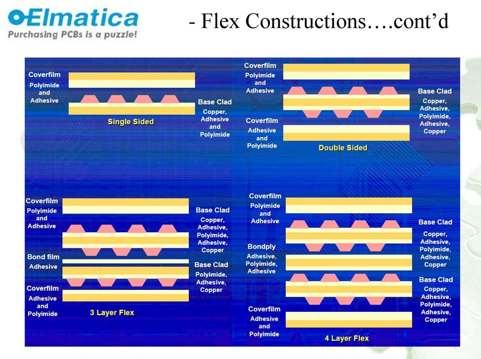
6 - Flex Constructions.cont d Application Attributes cont d - Single Sided Flex: This is a single copper layer/polyimide clad construction with a polyimide/adhesive coverlayer laminated to one side to allow access on one side only. - Dual Access Flex: This is the same construction as single sided flex but openings are created in the base polyimide/adhesive layers to allow access to the copper on both sides. - Double Sided Flex: This is a dual copper clad consisting of two layers of copper separated by adhesive and polyimide. Plated through holes (vias) complete the continuity from layer to layer. - Multilayer Flex: This is a combination of single sided and double sided clads to achieve the total layer count desired. Vias are incorporated to connect all layers. - Rigid Flex: This can be single or multiple layers of flex sandwiched between standard PCB materials to create rigid and flexible portions
 complete the continuity from layer to layer.")
7 - Flex Constructions.cont d

8 - Flex Constructions.cont d
9 - Flex Constructions.cont d Please note that coverfilm on flex areas shall stopp 1-2mm inside the rigid area. This is due to risk for delamination, See next slide.

10 - Flex Constructions.cont d It s important to pay attention to the area where the transition is made from flex to multilayer rigid construction. Rather than have coverfilm material extend completely through the entire circuit, it is reccomended to use what s called a bikini coverfilm. Just as a bikini swimsuit only covers the essentials, the bikini coverfilm extends just far enough into the multilayer area to provide reliable adhesion. The prepreg sheet is pre-cut to nest with the coverfilm. Why is this bikini cover-film/prepreg construction important? Combined with an adhesiveless base flexmaterial, this construction makes the plated holes more reliable, because there is no adhesive in the multilayer stackup. The vias are more likely to survive temperature cycling. More important, the designer must make sure that no vias are placed in this area. As shown, the plated holes should be far enough away from the transition area so that they don t travel through the coverfilm. The distance that the coverfilm extends into the multilayer area varies with different manu-facturers, but a good rule of thumb is to place via pads no closer than within 1-2mm from the edge of the multilayer area The fig. shows how the coverfilm layer barely encroaches into the multilayer section, being replaced byprepreg in the rigid area.

11 - How to s on Flex Design Design tips: For first time designers and engineers it is a good idea to become familiar with the specifications that have reference to Flex Circuit manufacturing. - IPC ( - IPC-2223 and IPC How do you want your flex to act or perform? - Develop your schematic. - Layer counts and trace densities will be calculated - Identify power, signal and ground traces - Understand your current requirements - Calculate conductor width needs

12 - How to s on Flex Design.cont d Flex Circuit Related Specifications: - IPC-2223 Sectional Design Standard for Flexible Printed Boards This specification has the most comprehensive tips for creating your design, and the following is based on this specification. - IPC-600 Manufacturability and Acceptability of Printed Circuits - IPC-FC-231 Flexible Bare Dielectrics for use in Flexible Printed Wiring - IPC-FC-232 Adhesive coated dielectric films for use in cover sheets for Flexible Printed Wiring - IPC-FC-233 Flexible Adhesive Bonding Films - IPC-FC-241 Metal clad flexible dielectric for use in fabrication of Flexible Printed Wiring - IPC-4562 Metal Foil for Printed Wiring Applications - IPC-T50-D Terms and definitions

13 - How to s on Flex Design.cont d Material Selection: - Attributes to consider flexibility, impedance, emi, to name a few. - Thinner material does not equate to cheaper. In most cases the thinner the copper and or polyimide / adhesive, the more expensive it is. BASE MATERIAL - The base material is the flexible polymer film that provides the foundation for the laminate. Under normal circumstances, the flex board base material provides most primary physical and electrical properties of the flexible board. - In the case of adhesiveless board constructions, the base material provides all of the characteristic properties. Although a wide range of thickness is possible, most flexible films are provided in a narrow range of relatively thin dimension, from 12 µm to 125µm. - While it is recognizable from experience that thinner materials are more flexible, it is worth remembering the engineering principle that with most materials, stiffness is proportional to the cube of thickness. This means that if the thickness is doubled, the material becomes eight times stiffer and will only deflect one-eighth as much under the same load.

14 - How to s on Flex Design.cont d Component termination method: - Surface mount, through hole, type of external connection, component support etc Level of electrical testing needed to assure that your design is acceptable: - Open and short test - Full functional test of all components.

15 - How to s on Flex Design.cont d -Your ultimate design is a collaboration across multiple engineering disciplines, Electrical, Mechanical and CAD. - Paper Doll -This term is used in conjunction with mechanical mock ups. This is a cost effective way of demonstrating form and fit and in most cases a good safety net to catch potential mechanical issues. - Trace/Space -While this is one of the building block of your design, special care must be given to the actual trace structure. Care must be taken to avoid sharp corners that is more typical on a rigid design.

16 - How to s on Flex Design.cont d -Filleted pad/ Hold Down Tabs -A major location for failure in a flex circuit is the interface between the board trace and the pad at the end. It is extremely critical that these interface points have transitional areas more commonly referred to as fillets. Hold down tabs add robustness to the copper pad. The additional hold down tab keeps the pad anchored during any subsequent assembly and rework. - Solder Relief -When placing pads in large copper traces or ground planes, solder relief pads should be created to allow for easier soldering of components. Large copper areas will sink heat away and cause cold or weak solder joints.

17 - How to s on Flex Design.cont d - Tear Stops - All inside corners MUST have a radius. In these cases a tear stop should be incorporated into the design as an added safety feature to guard against tearing or cracks propagating across a flex circuit. - Shields and Planes - Cross hatching can be used to create a shield or plane when flexibility is still a requirement. Shields can be created using copper or they can be screened on using conductive silver epoxy. - Grain Direction - When designing dynamic flex the copper grain direction must be taken into account. Rolled Annealed copper has a specific grain direction. To maximize the copper life you must flex in the direction of the grain.


18 - How to s on Flex Design.cont d - Material Utilization - This is the number one cost contributor to your design. During production, most manufacturers use a panel format. The more up per panel the lower the cost. Your goal should be the smallest form factor as possible. This can be achieved several ways but one creative way is to incorporate folds into your design. - Consider how flex-boards will be nested on a panel. - Follow recommended tolerances whenever possible. - If flex-boards have only a few layers, using stiffeners can be far less expensive than a rigid-flex board. - Remember Flex-boards both require and permit looser tolerances than rigid boards.


19 - How to s on Flex Design.cont d I-Beam - When routing your traces in a double sided flex it is best to stagger the traces to prevent an I-Beam effect. With the conductors stacked you run the risk of compression issues when bending to install. - Balance the track weights and material thicknesses on each side of the neutral bend axis. - Tracks should always be routed through bend areas as close to perpendicular (90 deg) as possible. - Track thickness and width should remain constant in bend areas. - Plated through holes should be kept out of the bend areas.

20 - How to s on Flex Design.cont d Conductor aspect - In a perfect world that rule of thumb is 4 times the track thickness (T). This is a safe rule, however your design will be pushed to ever increasingly smaller trace and space geometries. Ideal: Track width greater than 4x track thickness.

 be placed in the neutral axis of the flex cross section to provide optimal performance.")
21 - How to s on Flex Design.cont d -Balanced Board - A balanced board is important when flexibility is a concern. The copper conductors must (if possible) be placed in the neutral axis of the flex cross section to provide optimal performance. This allows the flex to operate without compression or tension while flexing

22 - How to s on Flex Design.cont d Electrical Considerations - Predictable electrical characteristics make flex boards an ideal choice for high-speed signal transmission. - Uniform spacing between tracks and grounds, continuous shield layers, and repeatable geometries are features that help control impedance and reduce crosstalk. - With flex boards, you can eliminate connectors and other transitions that contribute to signal attenuation. - Manufacturers can provide tight tolerances on track width, spacing, and distance to ground layers in order to meet your impedance requirements. - Actual impedance will also depend on the board s shape after installation. - Contact your manufacturer for advice on designing boards to specific electrical characteristics.
23 2-Layer vs. 3-Layer Designs2-Designs 2-layer Designs Provide More Flexibility - Require careful pad breakout design to maintain good return path integrity. - Lowest cost - Most non-emi critical applications can benefit from 2-layer flex designs 3-layer Designs Provide Better Shielding - Require cross-hatch to maintain flexibility - Require careful trace routing and pad breakout design to maintain good impedance and crosstalk control. - Highest performance
24 Multi-layer Requires Cross-Hatching of Planes to Maintain Flexibility - This can reduce performance if not well-designed. Two-layer can Use Solid Plane - Has performance advantage over 3 -layer - Wider traces for microstrip - Signals travel parially in air, wich has low loss. - Has increased emissions - Can be controlled by good design and layout practices
25 Traces misalignet with Cross Hatch

26 Microstrip sensitivity (4.5mil 0.11mm)
27 Copper vs. Silver inc. shilding
28 Silver Ink Flex Design Lower cost May be used for economic shielding in EMI sensitive applications - May be used over two or three layer copper flex for additional shielding in Mil/Aero applications Single-Ended Applications - Use below 250 MHz Differential Applications - Use below 1 GHz (2 Gbps) Current carrying power and ground should be placed on copper layers Limited flexure cycles
29 Insertion Loss ComparisonInsertion Comparison
30 - How to s on Flex Design.cont d Current Calculator - There are several ways to calculate current carrying capacity. One of the most popular is to use the nomograph published in IPC There is a version that can be accessed at:
31 - How to s on Flex Design.cont d Bend Radius: Single-layer: Double-layer: Multilayer: 06 board thickness (minimum) 12 board thickness (minimum) 20 board thickness (minimum) Circuit thickness is approximately 0.15mm per layer. Sharper, permanent bends are common for bend and stay applications Strain vs. Ductility: The bending of flex boards causes deformation, strain, and stresses in the circuit materials. The strains and stresses are functionally related for each material via the stress-strain diagram. The forces necessary to cause flexural deformation are small; the flexural deformation is determined by the imposed bend geometry.
32 - How to s on Flex Design.cont d Basic Manufacturing Flow-The sample flow depicts the process steps required to build a double sided- and Rigid-Flex circuit. Several inspection steps, as well as sub steps have been left off.
33 - Materials Material Selection Materials can range in a variety of attributes. You must have a clear understanding of exactly what type of performance you expect and/or desire in your application. Is a high flex life required, controlled impedance, ultra thin coppers, adhesiveless clads, or is it solely a cost driven design? The industry leader in flex circuit materials, DuPont Electronics. ( is often used.
34 - Materials.cont d Polyimide Films. - This is the material used as the base layer for both the copper clad and the coverfilm. The most common thicknesses are: ( Red is less common ) mm mm mm mm mm Adhesives - Adhesives are used to bond the polyimide film to the copper layer or board layer it is exposed to. Some of the typical adhesive types are: Acrylic, Modified Acrylic, Phenolic Butyral, Modified epoxy and PSA (Pressure sensitive adhesives). The most common thicknesses are mm mm mm - When it comes to temperature resistance, the adhesive is typically the performance-limiting element of a laminate, especially when polyimide is the base material. - As with base films, adhesives come in different thicknesses. The thickness selection is typically a function of the application. For example: Different adhesive thicknesses are commonly used in the creation of coverlayers in order to meet the fill demands of different copper-foil thicknesses that may be encountered. It is essential that you verify the chosen material availability from your manufacturer.
35 - Materials.cont d Metal (copper) Foils - A metal foil is most commonly used as the conductive element of a flexible laminate. The metal foil is the material from which the circuit paths normally are etched. Typical flex boards use RA (Rolled Annealed copper), although ED (Electro Deposited) coppers are used in adhesiveless clads. The thickness range can vary, but typical RA foils are 0.017mm (½ ounce), 0.035mm (1 ounce) and 0.070mm (2 ounce). LAMINATES - Metal foil clad laminates are the basic form of material used for most flexible board constructions. While copper foil dominates applications, other foils can be used. Typically, a laminate is created by bonding together a sandwich comprised of a base material, an adhesive and a metal foil. The stack is then subjected to sufficient heat and pressure in a laminating press to create a permanently bonded metal polymer laminate. In the case of adhesiveless laminate substrates, the adhesive is absent from the construction. Adhesiveless laminates can withstand higher temperatures.
36 - Materials.cont d LAMINATED COVERLAYERS - Normally, a coverlayer is a two-layer material comprised of a base material and a suitable thermosetting adhesive. However, suitable homogenous thermoplastic films may also be used as coverlayers. The coverlayer serves to protect the conductors of the finished flex board and help enhance flexibility. PHOTOIMAGEABLE COVERLAYERS - Another type of coverlayer for use in flex manufacture is a photoimageable coverlay. This product is akin to dry film solder mask. It requires vacuum lamination to assure a good seal around the board traces. Just like a photoimageable solder mask, the material is exposed and developed to provide access to board component attachment features..
37 - Materials.cont d COVERCOATS - The term covercoat is used to describe a range of thin coatings applied to the surface of conductors in lieu of a coverlayer. Although some suppliers of covercoat material have some impressive flex cycling data, covercoats are normally reserved for applications where no (or minimal) dynamic flexure is required. In manufacturing, covercoats normally are applied as a liquid by screen-printing and then either cured by heat or by exposure to UV radiation.
38 - Materials.cont d BONDPLIES - Bondplies are flex board construction elements comprised of a base film with an adhesive film cast on both sides. The adhesive element of the construction is typically a thermosetting material. While bondplies can be used for creating two-metal layer laminates, bondplies most typically are used as building blocks in the manufacture of some more complex flex structures such as multilayer flex and rigid flex boards.
39 - Materials.cont d CAST ADHESIVE FILMS - Cast adhesive films are freestanding adhesive materials. The films are most typically thermosetting adhesive films, which are cast onto a disposable carrier or release film. Cast adhesive fims are also often used to bond rigid stiffening materials to a flex board. They have also been used as replacement for bondplies in certain applications. PRESSURE-SENSITIVE ADHESIVES - Pressure-sensitive adhesives (PSAs) are a family of semi-permanent to permanent adhesive films on peelable carriers, which can be transferred directly to the surface of the flex board or other material for later attachment to another surface. Once the PSA is applied to the board, it can be bonded later to nearly any surface. However, most typically, pressure-sensitive adhesives, when used in flex circuit manufacture, are employed to attach stiffeners to flexible boards. There is also a special subset of the pressure-sensitive adhesive family that can be screen-printed directly onto the back surface of the flex board, and then cured to provide the necessary tacky finish by exposure to ultraviolet radiation. This method can be used to advantage in very-high-volume applications or where cost is kept to a desired minimum.
40 - Materials.cont d STIFFENER MATERIALS - While not an integral part of the flex board, stiffeners are an important element of flex board construction. Stiffening materials are used to reinforce flex circuits when and where required. Most commonly, stiffeners are under areas where electronic components are to be attached. They serve to support the weight of the components both through the assembly process and in the application. Stiffeners can be made of almost any material, including metal, plastic, resin-glass laminates or even additional layers of coverlayer material. The use of coverlayer material to stiffen areas of a flex is actually a very common practice. COMPONENT HOLES IN STIFFENER - Holes in the stiffener for through hole mounting of components, should be µm larger than the through holes in the flex board.
41 - Materials.cont d FILLET TRANSITION EDGE OF STIFFENER - Filleting of the transition edge of a stiffener with a resilient adhesive or epoxy is another common method of strain relieving boards. The small bead of a suitable polymer will provide a simple means of transitioning strain from the stiffener to the flex board.
42 - General Flex Circuit terms -Basic Glossary of Terms (see IPC-T50-D for complete list) Adhesive -Acrylic*, flame retardant, epoxy, epoxy prepreg, polyimide prepreg, phenolic ( * most common materials used for manufacturing flex circuitsfor max flexibility.) Annular Ring - This is the exposed copper ring surrounding a through hole. Artwork - This is the tool used to define circuit features. Typically CAD generated. Back Bared Pads - This is a flex that is typically single sided in construction but has the copper accessed from both sides. Back Side Access - This is a flex that is typically single sided in construction but has the copper accessed from both sides. Conductor / Track - The metallic path that carries electrical current.
43 - General Flex Circuit terms Cont d Track / Conductor Spacing - This is the distance between tracks measured at the foot (widest point) of the track. Track Conductor Width - This is the width of the track measured across the base of the track. Coverfilm - This is the insulating material, usually in a film format, that is laminated to the flex board to define solderable areas. Can be drilled, laser cut or chemically removed to create complex geometries. Dynamic - This is the term used to describe the intended use of the flex. Repeated flexing, as in a disk drive, requires a dynamic flex circuit. ED, Electro Deposited -This is the means by which copper is deposited on polyimide to create an adhesiveless clad.


44 - General Flex Circuit terms Cont d Hard Tooling - A term used to describe tooling used to fabricate flex boards typically when tight tolerances and or high volumes are required. HASL -This is the acronym for a soldering process. Hot Air Solder Level. (Often not ideal to use on flex boards) Hold Down Tabs -These are extensions of the copper pad and are used to help anchor the pad during soldering processes both in assembly and rework. I-Beam Effect -This is the result of stacking your conductors during your design. Subsequent flexing induces stress and compression, causing cracking to occur. Impedance - Basically this is the total effective resistance to AC current. It can be altered by changing conductor spacing, signal spacing relative to ground, material thicknesses.

45 - General Flex Circuit terms Cont d Nested Panel - This is the process by which the individual board is maximized on a panel. Pad - The end of a conductor usually configured to accept a component or to be attached to a device. PIC, Photoimagable Coverfilm - This is another means of defining your solderable areas. This material is apply in a clean room environment, exposed with an artwork and then developed. This allows for complex geometries not available from routing or other soft tooling means.

46 - General Flex Circuit terms Cont d Pads only Plate (button plate) -This is the process by which only the via and a small portion of the surrounding pad is plated in a double sided or multilayer flex. This limits the amount of plating a panel will see and allows the double sided flex board to still be somewhat flexible.

47 - General Flex Circuit terms Cont d Panel Plate - This is where the entire panel is plated increasing the total overall copper thickness.
 - This is a term used to describe the type of copper and it is actually the method by which the copper is flattened.")
48 - General Flex Circuit terms Cont d PSA (Pressure Sensitive Adhesive) - An adhesive used to bond stiffeners to specific regions of the flex circuit. RA (Rolled Annealed) - This is a term used to describe the type of copper and it is actually the method by which the copper is flattened. Through Hole/Vias - A plated hole in the panel that can be accessed through the coverfilm or can be tented over with the coverfilm. There are numerous versions of these. Blind Via - Typically a via that penetrates to several layers below but is covered up by the coverfilm Buried Via - A via that is set deep inside a multilayer with no access to the coverfilm Tented Via - A via that goes completely though the flex, but is covered by the coverfilm on both end limiting access.
49 - Capability Some safe values to use for design Panel size (is manufacturer dependent - Single sided through multilayer construction, 12 x 18 Drilled holes size - Plated or non-plated 0.25mm diameter - Tolerance of hole to hole is ± 0.1mm Aspect ratio (ratio of hole depth/hole diameter) - 10:1 maximum. Track width /space - Using ½ ounce (17um) thick copper, 0.1mm track/space - Using 1 ounce (35um) thick copper, 0.15mm track/space Conductor aspect ratio - For best producibility, design traces to be at least four times as wide as they are thick. In tight situations it can be successful to achieve : 1 ratio conductor widths. Layer count layers - Solid or cross hatched ground layers
50 - Capability Some safe values to use for design Stiffener - Epoxy-glass (FR-4), polyimide-glass, polyimide, copper, aluminum. Surface finishes - ENIG - Chemical Tin - Chemical Silcer - Hard Gold over Nickel - HASL / LF-HASL **** - OSP Outline tolerances: - SRD 0.38mm - Laser / Hard tool 0.10mm - CMD (chemical Milled die) 0.25mm Shield layers - Solid or grid patterned - copper foil or screened conductive ink.

51 - Capability Some safe values to use for design Fingers - Supported: 0.20mm minimum, center-to-center; - Unsupported: 0.50mm minimum, center-to-center.
52 - Design issues TEAR-RESISTANCE FEATURES IN FLEX DESIGN - All flex board designs should be made as tear-resistant as possible. While the material may not be intrinsically tear-resistant, tear-resistance can be improved by employing certain features in the design. There are several possible methods, described and illustrated below. All of the following techniques have been successfully used to help prevent tearing. One or more of the following techniques can be used: 1) Radius All Internal Corners The first line of defense against tearing is to make certain that all internal corners are provided with as generous a radius as possible. This design practice is the most important and simplest of all methods used to prevent tearing of the flex buard material.
53 - Design issues.cont d 2) Laminate Glass Fabric in Corners Glass cloths can be laminated into corners during the fabrication process. Though not flexible, this method has been shown to provide a very robust corner construction and has been favored in the past by military product designers. It is an expensive solution, however, because of the type of preparation required and should be used only after careful consideration of the alternatives. Use Fluoropolymer Coverlayer The use of fluoroplastics such as Teflon as coverlayers helps to improve tear resistance by virtue of the high tear resistance of the polymer itself. This is due to the fact that fluoropolymer tends to stretch rather than tear, adding toughness to the substrate. An additional benefit of using fluoropolymer coverlayers for those involved in high frequency design is that the dielectric constant of the coverlayer is much lower.
54 - Design issues.cont d 3) Use of Radiused Slots The use of slots with ends that have a radius to access relieved board features also can serve to provide tear resistance. Normally, such features can easily be provided for during the punching operation or other board fabrication process. 4,5) Drilled Holes at Corners or Ends of Slits Drilled or punched holes in corners or at the ends of access slits have been used with success when flexible appendages must be spaced close together. This method allows the greatest use of material, but the hole size chosen will impact tear resistance. If the hole is very small, the overall robustness will be reduced.
55 - Design issues.cont d 6) Aramid Fibers Inside Cut Line As an alternative to glass cloth, the use of aramid fibers routed through corners or along the entire outline of the flex board is a unique method to stop tearing. The thin polymer fibers have very high strength and are very pliable, minimally affecting flexibility. However, this is a labor intensive method and should only be specified with the knowledge of cost impact. 7) Leave Metal in Corners The board design should, if possible, have small areas of copper provided for at internal corners to serve as tear stops at the inside of corner radius. This serves to prevent further or imminent propagation of a tear through the polymer, should a tear in the material start.
56 - Design issues.cont d (1)Large radius in corner (2)Embedded glass cloth (3)Radiused slot (4)Hole in slit (5)Drilled hole at corner (6)Embedded aramid fiber (7)Extra copper in corner
57 - Design issues.cont d Proper circuit nesting can greatly improve panel yield and lower overall cost. If folding can be tolerated as an assembly operation, yield can be maximized. For dynamic flex board designs, the grain direction requirement may impact layout.

58 - Design issues.cont d Conductor width nomograph The nomograph is valid only for tracks with a polyimide cover layer not exposed conductors. The temperature rise curves only recognize heat generatedby the track itself. Heat from power dissipating components or nearby tracks on other layers is not included. Example #1: A current of 1 amp with ½ oz. copper and 30 C temp. rise, will require a track width of (1mm). Example #2: A 0.140" (0.36mm) wide track etched from 1 oz. Copper (0.0014") will produce a temperature rise of 10 C at 2.7 amp.

59 - Design issues.cont d It is best to specify round (instead of slotted), through-holes. This will reduce drillingtime and cost. Whenever possible, design pads larger than the access holes. If space is critial, use hold-down tabs. Hold-down tabs are especially important for single layer boards, because a single layer board does not have the added strength of plated through-holes. A variety of hold-down tab designs are available. Pad fillets improve etched yield and material strength. Fillets are appropriate when the pad diameter is greater than the connecting strand width. Acute angles at the interface between traces and pads are to be avoided by using fillets to minimize the concentration of stress at the interface.
60 - Design issues.cont d The steel rule die is a cost-effective tool for punching flex boards from their panel. Class-A tooling for flex circuit punching offers both high precision and long tool life. Example of an etched punch die tool
61 - Design issues.cont d Stiffeners in panelized form facilitates both the application of the flex board to the stiffener and subsequent component assembly. When the flex board and stiffener are bonded together, the resulting flex board panel can be processed much like a rigid board. Note that the adhesive is applied oversized and cut to dimension before the routing step is performed.
62 - Design issues.cont d STAGGERED LENGTH BOARDS (BOOKBINDER CONSTRUCTION) For ease of flexing multilayer and rigid flex designs, the use of staggered length design is commonly employed. The technique is accomplished by adding slightly to the length of each succeeding flex layer, moving away from the bend radius. Staggered length designs facilitate bending of the flex board. The circuit can only be bent in one direction by design. A common rule of thumb is to add length equal to roughly 1.5 times the individual layer thickness. Without staggered lengths, layer buckling occurs.
63 - Design issues.cont d Various flexing and bending methods large radius or hinge type flex Coiled flex Counter Rolling flex window shade flex Accordion flex Rolling flex

64 - Cost impact of layer count The information for the chart are taken from a sample of circuits built with standard materials. This chart is not intended to be used as a price guide. However, it does showthat circuit cost generally rises with layer count. It is in your best interest to consider all options to minimize cost. For example, use two circuits to do the job of one. Two double-layer circuits may be less expensive than one four-layer circuit. But the cost savings of the circuit may be offset by additional assembly requirements. Circuits can also be folded in order to save space and layers. Each situation is unique. A rela-tively small amount of time invested in project assessment canresult in significant savings overall.
65 - Documentation Needs for Flex Boards The documentation package for a flexible board is the means by which the needs and requirements of the user are communicated to the manufacturer. If the information presented is clear and easily understandable, the chances of getting the product you want on the first pass is greatly enhanced. But we have an idea that 80% of the flex documentation packages we receive require some sort of clarification. This is directly man-hours lost that could have been used to meet manufacturing targets. At a bare minimum, the circuit manufacturer needs to be given the following information in order to complete his manufacturing task properly:
66 - Documentation Needs.cont d -Class of product -Materials to be used for construction - base material and coverlayers - metal foil type and thickness - Definition of holes, hole position and hole size - Stackup showing no. of layers & cross sectional view - Marking requirements, materials and locations - Bend and Flex locations and direction of bend - Stiffener locations and bonding requirements - Special process and/ or finish requirements - Test point locations - Special testing requirements - Coverlayer or Covercoat opening locations - Board outline with datum and dimmensions - Tolerances for manufacturing - Hole tolerances - Physical dim. Tolerances - Critical dimensions, if any. The list of items just provided provides a solid base in terms of understanding the general nature of need for flex board design documentation. However the list does not detail all the potential documentation requirements or needs of all possible flexible circuit designs. This is a never-ending list. Designers will always have special needs for their particular board design.
67 - Documentation Needs.cont d DEFINE CLASS OF PRODUCT There are three generally-accepted classes of product as defined by IPC standards: Class 1, consumer products, Class 2, telecommunications, computers and general industrial, and Class 3, high-reliability. The definition of class will serve to provide guidelines as to how the product must be fabricated and inspected as well as provide performance requirements. DEFINE MATERIALS TO BE USED FOR CONSTRUCTION The materials to be used in construction of the circuit need to be defined to inform the manufacturer of which material the circuit should be made from. This includes issues of base polymer choice, adhesive type and copper foil type, along with the thickness of each of the above.
68 - Documentation Needs.cont d Definition of holes, hole position and hole size There is a need to define a hole count for each different hole size called out. This can usually be most easily accomplished by simply extracting data from digital files. The data are commonly used to help define the manufactured cost of the board. While the sales department may be interested in the hole count, manufacturing is interested in hole location in order to verify that holes and artwork are properly aligned. Hardcopy or digital information will work. These data can be extracted from drill files. Stackup showing no. of layers & cross sectional view This information serves the needs of both manufacturing and sales. The layer count provides an indication of board complexity to sales and a key descriptor of the product to manufacturing. The cross-sectional view of the board is required to provide a visual cue as to what the designer expects his finished product to look like on edge. This is helpful predicting overall thickness.
69 - Documentation Needs.cont d PROVIDE COVERLAYER OR COVERCOAT OPENING LOCATIONS The documentation package should also define the location of access points through the coverlayer or covercoat. In many cases, these will match the hole locations defined earlier, however, when SMDs are used, many other locations on the circuit will require access. PROVIDE CIRCUIT OUTLINE WITH DIMENSIONS AND DATUMS The final circuit outline is necessary to define the periphery of the circuit relative to the circuitry itself. These data are used to create the tooling required to remove the part from the panel. The datums are important reference points to facilitate measurement, and datums shall be inside the board rather than outside the board outline. This makes inspection easier.


70 - Documentation Needs.cont d MARKING REQUIREMENTS, MATERIALS AND LOCATIONS Marking requirements must be defined to provide the circuit manufacturer the information needed to locate accurately and mark properly specific locations on the circuit. The choice of type and color of marking ink must also be defined. BEND, FLEX AND CREASE LOCATIONS It is helpful to define the location of bend and flex areas as well as where crease lines may be required. This can be accomplished by placing special indicating features in the circuit artwork. It can also help the assembly process by providing information as to which direction a bend must take. For example, dotted lines could be used to indicate bends in one direction, and solid lines could then indicate bends in the opposite direction.
71 - Documentation Needs.cont d STIFFENER LOCATION AND BONDING REQUIREMENTS Location of flex circuit stiffeners and special bonding requirements or instructions should be provided in the documentation package. Requirements for special strain-relief techniques such as an epoxy bead along flex to rigid trans formations should also be mentioned here. SPECIAL PROCESSING AND/OR FINISH REQUIREMENTS If special processes are required such as the addition of special tear restraints or special finishes on the flex board, they should be marked. This includes request for solder plating, nickel or gold plating, and the use of special, Organic Solderable Protective coatings. The chemical surfaces is preferred on flex boards, due that molten solder finishes (HASL) can damage the flex board.
72 - Documentation Needs.cont d TOLERANCES FOR MANUFACTURING Manufacturing tolerances should be called out on the print. Most print formats provide a tolerance block near the title block for the drawing. Keep in mind that by nature of the product, flex circuit tolerances are or should be less stringent than those applied to rigid board constructions. As a result, the tolerance block should accurately reflect the capabilities of the finished flex product. TEST POINT LOCATIONS Test point locations, if restricted, should be defined either in the print or, more preferably, in a digital data format. The use of test nodes in place of 100% testing of all points on a circuit can help reduce testing cost by limiting test points only to those required. It is important to remember that test probes will likely leave physical indentations on the metal surface due to the softness of the flex circuit base material. If this will be cause for concern by receiving inspection, it should be fully discussed with the manufacturer. SPECIAL ELECTRICAL TESTING REQUIREMENTS Should they be required, any special electrical tests should be defined in the documentation. This includes such tests as TDR (Test Discrepancy Reports) or special high pot testing. Conditions of test, and test point locations, should also be thoroughly defined in advance.
Flex Circuit Design and Manufacture.
 Flex Circuit Design and Manufacture. Hawarden Industrial Park, Manor Lane, Deeside, Flintshire, CH5 3QZ Tel 01244 520510 Fax 01244 520721 Sales@merlincircuit.co.uk www.merlincircuit.co.uk Flex Circuit
Table of Contents. Flex Single-Side Circuit Construction. Rigid Flex Examples. Flex Double-Side Circuit Construction.
 Table of Contents Flex Single-Side Circuit Construction Flex Double-Side Circuit Construction Multilayer Flex Circuit Construction Rigid Flex Examples IPC Information Glossary Rigid-Flex Construction Base
Balancing the Electrical and Mechanical Requirements of Flexible Circuits. Mark Finstad, Applications Engineering Manager, Minco
 Balancing the Electrical and Mechanical Requirements of Flexible Circuits Mark Finstad, Applications Engineering Manager, Minco Table of Contents Abstract...............................................................................................
How to Build a Printed Circuit Board. Advanced Circuits Inc 2004
 How to Build a Printed Circuit Board 1 This presentation is a work in progress. As methods and processes change it will be updated accordingly. It is intended only as an introduction to the production
The Don ts of Better Flexible Circuit Design and Manufacture By Mark Finstad Friday, 01 June 2007
 The Don ts of Better Flexible Circuit Design and Manufacture By Mark Finstad Friday, 01 June 2007 Successful designs are soon forgotten but failures are remembered for years. Steering clear of these twelve
Bending, Forming and Flexing Printed Circuits
 Bending, Forming and Flexing Printed Circuits John Coonrod Rogers Corporation Introduction: In the printed circuit board industry there are generally two main types of circuit boards; there are rigid printed
COPPER FLEX PRODUCTS
 COPPER FLEX PRODUCTS WHY FLEX? Molex ible Printed Circuit Technology is the answer to your most challenging interconnect applications. We are your total solution for ible Printed Circuitry because we design
1 Guidelines for Flex Boards
 1 Guidelines for Flex Boards The following information about flex and rigid/flex should be included in order to complete manufacturing task: 1. class of product 2. materials to be used for construction
FLEXIBLE CIRCUITS MANUFACTURING
 IPC-DVD-37 FLEXIBLE CIRCUITS MANUFACTURING Below is a copy of the narration for DVD-37. The contents of this script were developed by a review group of industry experts and were based on the best available
Flexible Circuit Design Guide
 Flexible Circuit Design Guide Benefits of Flexible Circuitry A solution to a packaging problem Placement around edges and folds Ability to be used in 3 axes connections Reduce assembly costs Very little
Practical Design Guidelines for Flex
 CHAPTER 5 Practical Design Guidelines for Flex INTRODUCTION Flexible circuits are obviously unique among electronic packaging technologies in that they offer a wide variety of advantages unobtainable using
White Paper. Recommendations for Installing Flash LEDs on Flex Circuits. By Shereen Lim. Abstract. What is a Flex Circuit?
 Recommendations for Installing Flash LEDs on Circuits By Shereen Lim White Paper Abstract For the mobile market some PCB assemblies have been converted to flex circuit assemblies, in part because flex
Flexible Circuit Simple Design Guide
 Flexible Circuit Simple Design Guide INDEX Flexible Circuit Board Types and Definitions Design Guides and Rules Process Flow Raw Material Single Side Flexible PCB Single Side Flexible PCB (Cover layer
Good Boards = Results
 Section 2: Printed Circuit Board Fabrication & Solderability Good Boards = Results Board fabrication is one aspect of the electronics production industry that SMT assembly engineers often know little about.
T H A N K S F O R A T T E N D I N G OUR. FLEX-RIGID PCBs. Presented by: Nechan Naicker
 T H A N K S F O R A T T E N D I N G OUR TECHNICAL WEBINAR SERIES FLEX-RIGID PCBs Presented by: Nechan Naicker We don t just sell PCBs. We sell sleep. Cirtech EDA is the exclusive SA representative of the
Flexible Printed Circuits Design Guide
 www.tech-etch.com/flex Flexible Printed Circuits Design Guide Multilayer SMT Assembly Selective Plating of Gold & Tin-Lead Fine Line Microvias Cantilevered & Windowed Leads 1 MATERIALS CONDUCTOR Copper
Using Flex in High-Speed Applications
 feature Figure 1: An automotive flex circuit designed to fit into a tight form factor. Using Flex in High-Speed Applications by Glenn Oliver DuPont Electronics and Communications Copper clad circuits in
Redefining the Cost/Performance Curve for Rigid Flex Circuits
 Presented at IPC Expo 99 Redefining the Cost/Performance Curve for Flex Circuits James Keating, Robert Larmouth and Greg Bartlett Teledyne Electronic Technologies 110 Lowell Road Hudson, NH 03051 Phone:
San Francisco Circuits, Inc.
 Your Doorway to Innovation San Francisco Circuits, Inc. Bridging Concepts with Reality Flex PCB Introduction to Flex Circuits What is Flex Circuits? From Wikipedia - a technology for assembling electronic
An Introduction to Rigid-Flex PCB Design Best Practices
 An Introduction to Rigid-Flex PCB Design Best Practices Golden Rules for First Time Success in Rigid-Flex An Introduction to Rigid-Flex PCB Design Best Practices More designers increasingly face project
DFX - DFM for Flexible PCBs Jeremy Rygate
 DFX - DFM for Flexible PCBs Jeremy Rygate 1 Jeremy Rygate 30 years experience with Front End in the Electronics industry and PCB manufacturing. Experience in advanced PCBs, particularly Flex, Flex-rigid
Flexible Solutions. Hubert Haidinger Director PE/CAM BU Industrial & Automotive 5.June 2013. www.ats.net
 Flexible Solutions Hubert Haidinger Director PE/CAM BU Industrial & Automotive 5.June 2013 www.ats.net Austria Technologie & Systemtechnik Aktiengesellschaft Fabriksgasse13 A-8700 Leoben Tel +43 (0) 3842
Valu Builds for Rigid Flex
 s for Rigid Flex Stable, robust builds for cost effective rigid flex We have gathered a set of low cost standard materials, with yield friendly design guidelines, to produce a cost effective rigid flex
Basic Designs Of Flex-Rigid Printed Circuit Boards
 PCBFABRICATION Basic Designs Of Flex-Rigid Printed Circuit Boards Flex-rigid boards allow integrated interconnection between several rigid boards. This technology helps to reduce the number of soldered
Rigid-Flex Technology: Mainstream Use but More Complex Designs by John Isaac October 1, 2007
 Rigid-Flex Technology: Mainstream Use but More Complex Designs by John Isaac October 1, 2007 In the past, flex and rigid-flex technology was typically used in applications that could tolerate long design
Flex-Rigid Design Guide Part 1
 Flex-Rigid Design Guide Part 1 The trend to miniaturization in electronics continues. Integrated circuit board solutions are becoming more and more popular as a means of efficiently utilizing the even
Automating Inter-Layer In-Design Checks in Rigid-Flex PCBs
 Automating Inter-Layer In-Design Checks in Rigid-Flex PCBs By Ed Hickey, Product Engineering Director, Cadence Flexible PCBs (flex/rigid-flex) make it possible to create a variety of products that require
CHAPTER 5. OVERVIEW OF THE MANUFACTURING PROCESS
 CHAPTER 5. OVERVIEW OF THE MANUFACTURING PROCESS 5.1 INTRODUCTION The manufacturing plant considered for analysis, manufactures Printed Circuit Boards (PCB), also called Printed Wiring Boards (PWB), using
Miniaturizing Flexible Circuits for use in Medical Electronics. Nate Kreutter 3M
 Miniaturizing Flexible Circuits for use in Medical Electronics Nate Kreutter 3M Drivers for Medical Miniaturization Market Drivers for Increased use of Medical Electronics Aging Population Early Detection
Flexible Circuit and Heater DESIGN GUIDE
 WE GO WHERE OTHERS WILL NOT Flexible Circuit and Heater DESIGN GUIDE ISO 9001:2008, ISO 14001:2004, ISO 13485, TS 16949, ROHS COMPLIANT, ITAR REGISTERED, UL REGISTERED, FDA REGISTERED, IPC MEMBER, BBB
Rogers 3003, 3006, 3010, 3035, 3203, 3206, 3210
 Stocked Materials: RIGID STANDARD FR4 High Tg 170c Black FR4 Polyclad 370HR (Lead Free) HIGH RELIABILITY Polyimide (Arlon 85N, Isola P96) BT (G200) HIGH FREQUENCY: Park Nelco 4000-13, 4000-13si Getek Gore
FABRICATION 2011 SERVICES TECHNOLOGIES CAPABILITIES INDUSTRY
 FABRICATION 2011 SERVICES 24HRS - 5 DAYS ON QUICK TURN PROTOTYPE Dear Customer, We would like to take this opportunity to welcome you and thank you for looking to ASA PCB as your Printed Circuit Manufacturing
Thermal Management Solutions for Printed Circuit Boards used in Digital and RF Power Electronics and LED assemblies
 Thermal Management Solutions for Printed Circuit Boards used in Digital and RF Power Electronics and LED assemblies Sandy Kumar, Ph.D. Director of Technology American Standard Circuits, Inc 3615 Wolf Road
DRIVING COST OUT OF YOUR DESIGNS THROUGH YOUR PCB FABRICATOR S EYES!
 4/3/2013 S THROUGH YOUR PCB FABRICATOR S EYES! Brett McCoy Eagle Electronics Schaumburg IL. New England Design and Manufacturing Tech Conference Brett McCoy: Vice President / Director of Sales Circuit
Flex Circuit Design Guide
 TECHNICAL SPECIFICATION FC302 Flex Circuit Design Guide www.minco.com Flex Circuits Thermofoil Heaters Sensors Instruments Minco Flex Circuits Table of Contents Introduction Table of Contents......................................2
Flex Circuits Design Guide. Design Guidelines for Highly Reliable Flexible Printed Circuits Optimized for Manufacturability
 Flex Circuits Design Guide Design Guidelines for Highly Reliable Flexible Printed Circuits Optimized for Manufacturability The purpose of this design guide is to enable you to design a highly reliable,
PCi Valu Builds for Rigid Flex
 PCi Valu Builds for Rigid Flex Stable, robust builds for cost effective rigid flex. PCi Valu Builds Overview Valu Builds are a set of low cost materials, with yield friendly design guidelines, to produce
Comprehensive Analysis of Flexible Circuit Materials Performance in Frequency and Time Domains
 Comprehensive Analysis of Flexible Circuit Materials Performance in Frequency and Time Domains Glenn Oliver and Deepu Nair DuPont Jim Nadolny Samtec, Inc. glenn.e.oliver@dupont.com jim.nadolny@samtec.com
Extending Rigid-Flex Printed Circuits to RF Frequencies
 Extending -Flex Printed Circuits to RF Frequencies Robert Larmouth Teledyne Electronic Technologies 110 Lowell Rd., Hudson, NH 03051 (603) 889-6191 Gerald Schaffner Schaffner Consulting 10325 Caminito
Dynamic & Proto Circuits Inc. Corporate Presentation
 Dynamic & Proto Circuits Inc. Corporate Presentation 1 DAPC Facility 54,000 Sq.ft./6,000 Sq.M 2 Multilayer Process 3 Solder Mask Options BLUE BLACK RED GREEN DRY FILM CLEAR 4 Investing in Technology New
Printed Circuit Boards
 Printed Circuit Boards Luciano Ruggiero lruggiero@deis.unibo.it DEIS Università di Bologna Flusso di progetto di un circuito stampato 1 Specifications Before starting any design, you need to work out the
Designing Flex and Rigid Flex Products for High Reliability Applications. Adeodato Vigano Circuits, LLC
 Designing Flex and Rigid Flex Products for High Reliability Applications Adeodato Vigano Circuits, LLC Benefits and applications The Basics Design considerations Design for manufacturing Materials properties
Safety Certification for Lead Free Flexible and Rigid-Flex PCBs
 Safety Certification for Lead Free Flexible and Rigid-Flex PCBs Crystal Vanderpan Underwriters Laboratories Inc. March 27, 2007 Crystal Vanderpan Principal Engineer for Printed Circuit Technologies Joined
Count on Optima Technology Associates to meet your requirements
 Since 1995, Global Resources, Local Support When you need quality Printed Circuit Boards To Spec On Time On Budget Count on Optima Technology Associates to meet your requirements Optima Technology Associates,
Microwave Multi-layer Printed Circuit Boards
 Microwave Multi-layer Printed Circuit Boards MicroAPS at IEEE MTT-S IMS in Fort Worth, TX Ed Sandor, Manager of Application Engineering, Taconic Advanced Dielectric Division June 9, 2004 Abstract Over
 Preface xiii Introduction xv 1 Planning for surface mount design General electronic products 3 Dedicated service electronic products 3 High-reliability electronic products 4 Defining the environmental
Eatman Associates 2014 Rockwall TX 800-388-4036 rev. October 1, 2014. Striplines and Microstrips (PCB Transmission Lines)
") Eatman Associates 2014 Rockwall TX 800-388-4036 rev. October 1, 2014 Striplines and Microstrips (PCB Transmission Lines) Disclaimer: This presentation is merely a compilation of information from public
Eatman Associates 2014 Rockwall TX 800-388-4036 rev. October 1, 2014 Striplines and Microstrips (PCB Transmission Lines) Disclaimer: This presentation is merely a compilation of information from public
Module No. # 06 Lecture No. # 31 Conventional Vs HDI Technologies Flexible Circuits Tutorial Session
 An Introduction to Electronics Systems Packaging Prof. G. V. Mahesh Department of Electronic Systems Engineering Indian Institute of Science, Bangalore Module No. # 06 Lecture No. # 31 Conventional Vs
Graser User Conference Only
 Miniaturization- Rigid-Flex Design with Allegro Jonathan Lee / Graser 31/Oct/2014 Rigid-Flex Design with Allegro Miniaturization Design Miniaturization through Rigid-Flex Rigid-Flex Design Flow Miniaturization
This presentation is courtesy of PCB3D.COM
 Printed Circuit Board Design, Development and Fabrication Process This presentation is courtesy of PCB3D.COM Steve Rose Printed Circuit Board Design Engineer Slide 1 Introduction PCB 101 This presentation
Keeping Current to Stay Competitive in Flex PCB Laser Processing
 White Paper Keeping Current to Stay Competitive in Flex PCB Laser Processing Market Drivers, Trends and Methodologies ESI by Patrick Riechel, PCB Product Manager The push for smaller, cheaper and more
Historical production of rigid PCB s
 Historical production of rigid PCB s The Printed Circuit Board (PCB) The PCB What is a Printed Circuit Board? Green plastic thing with holes!! (green plastic syndrome) Platform for components Image with
Athena is the name given to our assortment of electronic tapes. products of the very highest quality. These tapes both conduct and
 Electric Athena. Athena is the name given to our assortment of electronic tapes products of the very highest quality. These tapes both conduct and insulate against electricity, in addition to warmth and
PCB Board Design. PCB boards. What is a PCB board
 PCB Board Design Babak Kia Adjunct Professor Boston University College of Engineering Email: bkia -at- bu.edu ENG SC757 - Advanced Microprocessor Design PCB boards What is a PCB board Printed Circuit Boards
Introduction to Photolithography Concepts via printed circuit board (PCB) manufacturing. PCB Background Information (courtesy of Wikipedia)
 manufacturing. PCB Background Information (courtesy of Wikipedia)") Introduction to Photolithography Concepts via printed circuit board (PCB) manufacturing Introduction As you saw on the video (http://www.youtube.com/watch?v=9x3lh1zfggm), photolithography is a way to nanomanufacture
Introduction to Photolithography Concepts via printed circuit board (PCB) manufacturing Introduction As you saw on the video (http://www.youtube.com/watch?v=9x3lh1zfggm), photolithography is a way to nanomanufacture
Flex-Circuit Design Guide
 APPLICATION AID #24 Minco 3/2000 920612-5 Flex-Circuit Design Guide All the benefits of a printed circuit board... The purpose of this design guide is to enable you to design a high-quality, manufacturable
Amphenol Sincere. Electronic Integration & Flexible Printed Circuits. Aerospace. Health Care. Heavy Equipment HEV. Industrial
 Amphenol Sincere Health Care Aerospace Heavy Equipment HEV Industrial Electronic Integration & Flexible Printed Circuits About Amphenol The second largest manufacturers of interconnect products 87 worldwide
Multi-Flex Circuits Aust.
 Contents: Base Materials Laminate Prepreg Panel Size (Utilization) Multilayer Layup N.C. Drilling Pattern design Impedance control Solder mask type Legend PCB Finishing Gold Plating Profiling Final testing
Design for Manufacturing
 2 Design for Manufacturing This chapter will address the fabrication process of the PCB and the requirements of the manufacturer. Manufacturers are separated by their limitations or constraints into categories
Connector Launch Design Guide
 WILD RIVER TECHNOLOGY LLC Connector Launch Design Guide For Vertical Mount RF Connectors James Bell, Director of Engineering 4/23/2014 This guide will information on a typical launch design procedure,
Solid shape molding is not desired in injection molding due to following reasons.
 PLASTICS PART DESIGN and MOULDABILITY Injection molding is popular manufacturing method because of its high-speed production capability. Performance of plastics part is limited by its properties which
The Company. Nujay was established in 2001.
 PRESENTATION The Company Nujay was established in 2001. We provide resources, expertise and global connections to the customers, who are seeking high quality products at competitive price. We have 35 years
Make up Epoxy adhesive
 Epoflex Base Materials series of MSC Polymer AG offers flexible base materials from simple single side flexible boards, flex-rigid applications up to highly complex multilayer boards. The dielectric is
PRINTED CIRCUIT BOARD SURFACE FINISHES - ADVANTAGES AND DISADVANTAGES
 PRINTED CIRCUIT BOARD SURFACE FINISHES - ADVANTAGES AND DISADVANTAGES By Al Wright, PCB Field Applications Engineer Epec Engineered Technologies Anyone involved within the printed circuit board (PCB) industry
A SURVEY AND TUTORIAL OF DIELECTRIC MATERIALS USED IN THE MANUFACTURE OF PRINTED CIRCUIT BOARDS.
 A SURVEY AND TUTORIAL OF DIELECTRIC MATERIALS USED IN THE MANUFACTURE OF PRINTED CIRCUIT BOARDS. By Lee W. Ritchey, Speeding Edge, for publication in November 1999 issue of Circuitree magazine. Copyright
Flexible Circuits, Inc. Design Guide
 Page 1 of 68 Foreword Flexible Circuits, Inc. produces high reliability flexible printed wiring interconnects. We are a MIL-P-50884 and IPC 6013 certified manufacturer. To provide this type of performance
Desmear and Plating Through Hole Considerations and Experiences for Green PCB Production
 Desmear and Plating Through Hole Considerations and Experiences for Green PCB Production Gerd Linka, (Neil Patton) Atotech Deutschland GmbH Berlin, Germany Abstract With the latest legislations from RoHS
Flexible Circuits and Interconnect Solutions More than a manufacturer
 Flexible Circuits and Interconnect Solutions More than a manufacturer HISTORY Currently 150 employees Focussed on Flex Technologies & Assembly Largest flex circuit manufacturer in the UK 3 rd /4 th largest
Printed Circuit Design Tutorial
 Printed Circuit Design Tutorial By Gold Phoenix Technology Tech Center, sales@goldphoenixpcb.biz Gold Phoenix has been sale PCB board in North America since 2003, during these years we received a lot of
Fabrication of Embedded Capacitance Printed Circuit Boards
 Presented at IPC Printed Circuits EXPO 2001 www.ipcprintedcircuitexpo.org Fabrication of Embedded Capacitance Printed Circuit Boards Joel S. Peiffer 3M St. Paul, MN Abstract Embedding capacitor materials
Auditing a Printed Circuit Board Fabrication Facility Greg Caswell
 Auditing a Printed Circuit Board Fabrication Facility Greg Caswell Introduction DfR is often requested to audit the PCB fabrication process of a customer s supplier. Understanding the process variations
3 Embedded Capacitor Material
 3 Embedded Capacitor Material Design and Processing Guidelines for Printed Circuit Board Fabricators Effective date: March 2004 Contents Overview Material Handling Process Compatibility Standard vs. Sequential
General-purpose flexible circuit
 The circuit board, coiled to show its flexibility, was made from six layers of a low-outgassing material for a medical device. Unusual circuits call for unusual materials Some flex circuits work in medical
1. Single sided PCB: conductors on only one surface of a dielectric base.
 The Department of Electrical Engineering at IIT Kanpur has a variety of devices and machines to produce single layer, double layer plated through printed circuit boards (PCBs), multi layer (max 8 layers)
Chapter 14. Printed Circuit Board
 Chapter 14 Printed Circuit Board A printed circuit board, or PCB, is used to mechanically support and electrically connect electronic components using conductive pathways, or traces, etched from copper
IIB. Complete PCB Design Using OrCAD Capture and PCB Editor. Kraig Mitzner. ~»* ' AMSTERDAM BOSTON HEIDELBERG LONDON ^ i H
 Complete PCB Design Using OrCAD Capture and PCB Editor Kraig Mitzner IIB ~»* ' AMSTERDAM BOSTON HEIDELBERG LONDON ^ i H NEW YORK * OXFORD PARIS SAN DIEGO ШШЯтИ' ELSEVIER SAN FRANCISCO SINGAPORE SYDNEY
3M Electrically Conductive Adhesive Transfer Tape 9703
 Technical Data April 2011 M Electrically Conductive Adhesive Transfer Tape 970 Product Description M Electrically Conductive Adhesive Transfer Tape 970 is a pressure sensitive adhesive (PSA) transfer tape
Flexible Circuit & Heater Design Guide
 Flexible Circuit & Heater Design Guide Download from our website: www.allflexinc.com Check out the online design course: www.designingflexiblecircuits.com www.allflexinc.com ISO 9001: 2008 AS9100C MIL-P-50884E
Quality assurance of flex circuits in the SCT barrel hybrid production
 Quality assurance of flex circuits in the SCT barrel hybrid production ATLAS Project Document No. Institute Document No. Created: dd/mm/yy Modified: dd/mm/yy Page: 1 of 11 DRAFT Quality assurance of flex
Aspocomp, PCBs for Demanding Applications
 HDI PIIRILEVYT Aspocomp, PCBs for Demanding Applications Automotive Electronics Industrial Electronics Mobile Devices Base Station Photos ABB, Aspocomp, Vacon and Wabco PCBs for Base Stations and Other
Ultra Reliable Embedded Computing
 A VersaLogic Focus on Reliability White Paper Ultra Reliable Embedded Computing The Clash between IPC Class 3 Requirements and Shrinking Geometries Contents Introduction...1 Case in Point: IPC Class 3
HDI. HDI = High Density Interconnect. Kenneth Jonsson Bo Andersson. NCAB Group
 HDI HDI = High Density Interconnect Kenneth Jonsson Bo Andersson NCAB Group Definitions / Standards (IPC) Pros & Cons Key equipment Build-ups Choice of material Design rules IPC HDI reliability (µvia stacked
(11) PCB fabrication / (2) Focused assembly
 PCB fabrication / (2) Focused assembly") Company Fact Sheet TTM Technologies, Inc. is a world-wide leader in the manufacture of technologically advanced PCBs, backplane and sub-system assemblies. Our Global Presence / Local Knowledge approach
Company Fact Sheet TTM Technologies, Inc. is a world-wide leader in the manufacture of technologically advanced PCBs, backplane and sub-system assemblies. Our Global Presence / Local Knowledge approach
3835 West Conflans, Irving, Texas 75061 sales@multilayer.com Call Us at (972) 790-0062 Fax (972) 790-0293
 790-0062 Fax (972) 790-0293") Multilayer Technology An AS9100 & ISO 9001:2008 Company Multilayer Technology is a full service PCB provider specializing in high quality, high density, quick turn fabrication for time-critical solutions.
Multilayer Technology An AS9100 & ISO 9001:2008 Company Multilayer Technology is a full service PCB provider specializing in high quality, high density, quick turn fabrication for time-critical solutions.
Polymer Termination. Mechanical Cracking 2. The reason for polymer termination. What is Polymer Termination? 3
 Polymer Termination An alternative termination material specifically designed to absorb greater levels of mechanical stress thereby reducing capacitor failures associated with mechanical cracking Mechanical
PCB Fabrication Enabling Solutions
 PCB Fabrication Enabling Solutions June 3, 2015 Notice Notification of Proprietary Information: This document contains proprietary information of TTM and its receipt or possession does not convey any rights
The Problem with UL Approval of Rigid Flex Circuits
 A Printed Circuits, Inc. White Paper 1200 West 96 th Street Minneapolis, Minnesota 55431 952.888.7900 PrintedCircuits.com The Problem with UL Approval of Rigid Flex Circuits By Bob Burns, National Sales
Rigid-Flex PCB Right the First Time - Without Paper Dolls
 As originally published in the IPC APEX EXPO Conference Proceedings. Rigid-Flex PCB Right the First Time - Without Paper Dolls Benjamin Jordan Altium Inc. Abstract The biggest problem with designing rigid-flex
PROPERTIES OF MATERIALS
 1 PROPERTIES OF MATERIALS 1.1 PROPERTIES OF MATERIALS Different materials possess different properties in varying degree and therefore behave in different ways under given conditions. These properties
A Novel Flex Circuit Area-Array Interconnect System for a Catheter-Based Ultrasound Transducer
 Presented at IMAPS 2002 Denver, Colorado September 5, 2002 (Best of Session Award) A Novel Flex Circuit Area-Array Interconnect System for a Catheter-Based Ultrasound Transducer Jeff Strole*, Scott Corbett*,
PRINTED CIRCUIT BOARD DESIGN AND MANUFACTURING CORP.
 PRINTED CIRCUIT BOARD DESIGN AND MANUFACTURING CORP. Corporate Information Established in 2004 Headquarter office in San Jose, CA Production factory located in Binh Duong, Vietnam - Center of hi-tech industrial
Flexible Circuits, Inc. Manufacturing Guide
 Page 1 of 66 Foreword Flexible Circuits, Inc. produces high reliability flexible printed wiring interconnects. We are a MIL-P-50884 and IPC 6013 certified manufacturer. To provide this type of performance
WELCOME TO VIASION. www.viasion.com
 WELCOME TO VIASION www.viasion.com BRIEF INTRODUCTION Viasion Technology Co., Ltd is a professional Printed Circuit Board (PCB) manufacturer in China. With around 1500 employees totally in 2 different
Five Year Projections of the Global Flexible Circuit Market
 Five Year Projections of the Global Flexible Circuit Market Robert Turunen and Dominique Numakura, DKN Research And James J. Hickman, PhD, Hickman Associates Inc Summary A new market research process has
MULTI-FLEX CIRCUITS AUSTRALIA. International Suppliers of PRINTED CIRCUIT BOARDS
 MULTI-FLEX CIRCUITS AUSTRALIA International Suppliers of PRINTED CIRCUIT BOARDS AUSTRALIA Multi-Flex Circuits Australia Leading suppliers of HIGH QUALITY PRINTED CIRCUIT BOARDS for every purpose OUR COMMITMENT
High Density SMT Assemblies Based on Flex Substrates
 High Density SMT Assemblies Based on Flex Substrates Robert Larmouth, James Keating Teledyne Electronic Technologies 110 Lowell Rd., Hudson, NH 03051 (603) 889-6191 Abstract The industry trend to shrink
What is surface mount?
 A way of attaching electronic components to a printed circuit board The solder joint forms the mechanical and electrical connection What is surface mount? Bonding of the solder joint is to the surface