~ llll III II II III IMI II I II I II European Patent Office Office europeen des brevets (11) EP B1 EUROPEAN PATENT SPECIFICATION
|
|
|
- Myron Edgar Hardy
- 8 years ago
- Views:
Transcription
1 (19) J (12) ~ llll III II II III IMI II I II I II European Patent Office Office europeen des brevets (11) EP B1 EUROPEAN PATENT SPECIFICATION (45) Date of publication and mention (51) nt. CI.6: B29C 45/27 of the grant of the patent: Bulletin 1997/05 (21) Application number: (22) Date of filing: (54) Printed circuit board for injection molding system Leiterplatte fur Spritzgiesssystem Plaque a circuit imprime pour systeme de moulage par injection (84) Designated Contracting States: AT BE CH DE DK ES FR GB GR IE IT LI LU NL PT SE (30) Priority: US (43) Date of publication of application: Bulletin 1994/28 (73) Proprietor: HUSKY INJECTION MOLDING SYSTEMS LTD. Bolton Ontario L7E 5S5 (CA) (72) Inventor: Schmidt, Harald Georgetown, Ontario L7G 4W1 (CA) (74) Representative: Patentanwalte Breiter + Wiedmer AG Seuzachstrasse 2 Postfach Neftenbach/Zurich (CH) (56) References cited: EP-A FR-A CO CO o CO o CO o Q_ LU Note: Within nine months from the publication of the mention of the grant of the European patent, any person may give notice to the European Patent Office of opposition to the European patent granted. Notice of opposition shall be filed in a written reasoned statement. It shall not be deemed to have been filed until the opposition fee has been paid. (Art. 99(1) European Patent Convention). Printed by Rank Xerox (UK) Business Services /3.4
 Priority: 10.12.1992 US 988863 (43) Date of publication of application: 13.07.")
2 1 EP B1 2 Description BACKGROUND OF THE INVENTION 1. Field of the Invention s The invention relates to the field of injection molding and, more particularly, to a printed circuit board wiring system for nozzle heaters of an injection molding system Description of the Related Art In the field of plastic injection molding, hot runner or "runnerless" injection molding machines are well known is and commonly used. In these machines, each cavity of a mold is served, usually by a heated nozzle or "drop" which delivers melted resin from channels in a heated manifold to the respective mold. Recent developments have provided injection molding machines where each 20 nozzle is independently heated and controlled. This independent temperature control is achieved by providing a heater and a temperature sensing device such as a thermocouple at each nozzle, and wiring each heater and thermocouple to a power source/controller which 25 supplies power to the heaters and reads the information supplied by the thermocouples. In a typical 96 cavity mold, however, 192 heater wires and 192 thermocouple wires are necessary to operate the nozzles. Conventionally, these wires are run through channels in the 30 mold manifold plate. This set up, however, requires about 460 m (1500 feet) of wire, and would typically require about 16 hours to set up. Further, a defective wire is very difficult to locate, and replacement usually involves splicing of the wire. Splices, however, are noto- 35 rious trouble spots for further problems, and also take up extra space in the already overcrowded wiring channels, which are kept to a minimum size in order to maintain the structural strength of the mold manifold plate. Replacing a defective heater also involves threading a 40 new pair of wires through the existing mass of wiring. European Patent Application No , published January 29, 1992, provides a pre-wired hot runner system. In this system, heater wiring is routed in a wiring frame and connected to individual heaters with 45 nuts at each terminal, and forms a series of closed conduits connected to a main junction box. The abovedescribed problems encountered with replacing a faulty wire are not addressed by the European Application. Further, due to the necessity of minimizing the size so of wiring channels in the mold manifold plate, the length of each wire must be carefully optimized in a pre-wired system, resulting in a non-flexible wiring system useful only for a specific number and configuration of cavities. It is desirable to provide a wiring system for an 55 injection molding machine which overcomes the aforedescribed problems with wiring. Accordingly, it is the principal object of the present invention to provide a wiring system for an injection molding machine which avoids the use of an excessive mass of wiring. It is a further object of the present invention to provide such a system which minimizes the size of wiring channels formed in the mold manifold plate. It is a still further object of the present invention to provide such a system which is serviceable from the front of the machine while installed. It is another object of the present invention to provide such a system wherein splices are not necessary to correct faulty wiring. It is still another object of the present invention to provide such a system wherein connection of heaters to the wiring system is achieved through conveniently connected and disconnected plugs. Other objects and advantages will appear hereinbelow. SUMMARY OF THE INVENTION The foregoing objects are readily achieved by the present invention, wherein printed circuit boards are utilized to avoid the problems associated with conventional wiring. According to the invention, an injection molding system comprises: a mold manifold plate housing a plurality of injection molding nozzles and housing heaters for the plurality of injection molding nozzles; at least one printed circuit board associated with the mold manifold plate; and a power source; wherein the at least one printed circuit board electrically connects the power source with the heaters. Each printed circuit board preferably comprises at least one power layer printed with a plurality of power supply tracks, the power supply tracks being connected at a first end to the power source and at a second end to a respective heater. Each nozzle preferably has a respective heater and further has a respective temperature sensing means, the printed circuit board having at least one power layer printed with a plurality of power supply tracks and at least one sensor layer printed with a plurality of sensor tracks, the power supply tracks being connected at a first end to the power source and at a second end to a respective heater, the sensor tracks being connected at a first end to a respective temperature sensing means, and at a second end to a controlling means. BRIEF DESCRIPTION OF THE DRAWINGS A detailed description of the preferred embodiments of the invention follows, with reference to the attached drawings, wherein: Figure 1 is a perspective view, partially in section, of an injection molding system according to the invention; Figure 2 is a perspective view, partially in section, of a printed circuit board for an injection molding sys- 2

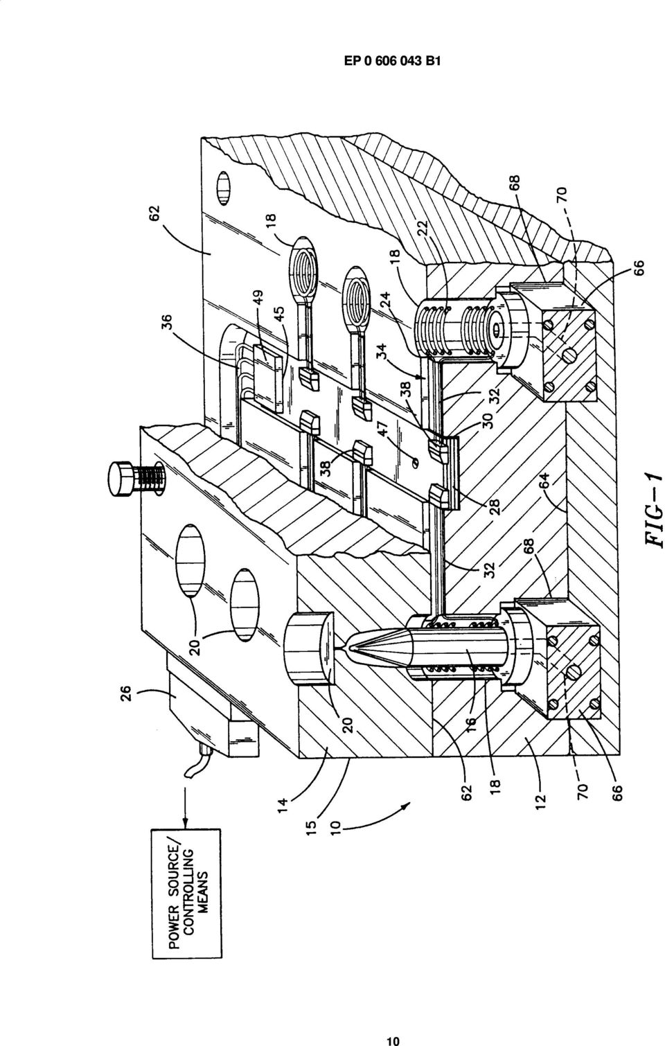
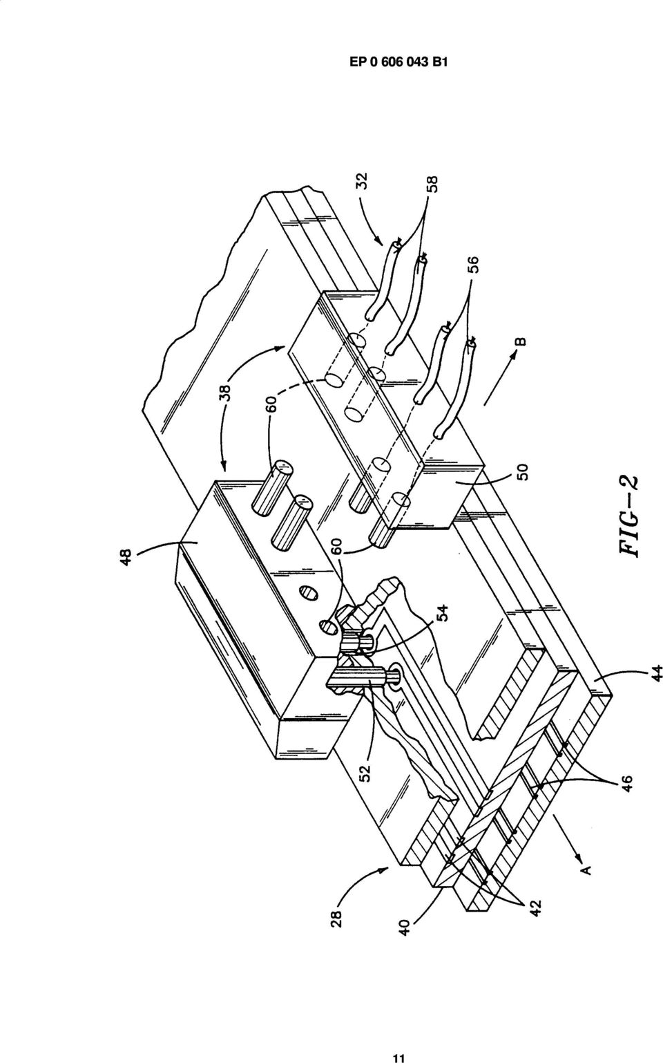
3 3 EP B1 4 tern according to the invention; Figure 3 is a schematic view of a layer of a printed circuit board according to the invention; and Figure 4 is a schematic view of an alternate embodiment of the invention. DETAILED DESCRIPTION OF THE PREFERRED EMBODIMENTS The invention relates to the field of plastic injection 10 molding, especially to hot runner or "runnerless" injection molding machines and, more particularly, to a wiring system for an injection molding machine having individually heated and controlled nozzles. According to the invention, printed circuit boards are used to provide is electrical connection in the injection molding machine in a more reliable, space efficient, and readily serviceable manner. Figure 1 shows an injection molding system 10 having a mold manifold plate 1 2, a mold cavity plate 1 4, and 20 a plurality of nozzles 16 disposed in wells 18 spaced about mold manifold plate 12. As is well known, melted resin or plastic is injected through nozzles 16 and into cavities 20 of mold cavity plate 1 4 in order to injection mold the articles being manufactured. Each nozzle 1 6 is 25 heated by heating means such as, for example, a heater 22 disposed in each well 18. Any conventional heater may be used, such as a coil heater as shown schematically in the drawing. The temperature of each nozzle 16 is preferably monitored by a temperature sensing 30 means such as thermocouple 24, which may also be mounted in well 18. In this manner, the temperature of each nozzle 16 and, therefore, the temperature of melted resin supplied through nozzle 16, is individually monitored. 35 Conventionally, wiring of heaters 22 and thermocouples 24 involves running an unwieldy mass of wires through wiring channels in the mold manifold plate, resulting in numerous problems and complications as discussed above. 40 According to the invention, heaters 22 and thermocouples 24 are connected to a mold connector 26 through printed circuit boards 28. Printed circuit boards 28 are mounted in association with system 10, preferably in association with mold manifold plate 12, so as to 45 electrically connect heaters 22 and thermocouple 24 with a power source through mold connector 26. Printed circuit boards 28 are preferably mounted in at least one circuit board channel 30, formed on mold manifold plate 12. Printed circuit boards 28 are provided, according to so the invention, so as to markedly decrease the space formerly required with conventional wiring systems. Thus, mold manifold plate 12 can be provided having circuit board channel 30 of a smaller dimension than the conventional channels used for wiring, thus providing a ss mold manifold plate 12 having a greater structural strength. One or more circuit board channels 30 may be provided on mold manifold plate 12, preferably between s rows of wells 18, so that heaters 22 and thermocouples 24 in wells 18 can be conveniently connected to printed circuit boards 28. Each heater 22 and thermocouple 24 preferably has a connector, such as connector wiring 32, for connection to printed circuit boards 28. Connector wiring 32 may preferably be disposed in additional channels 34, also formed on mold manifold plate 12, and preferably intersecting circuit board channel 30. It should be noted, of course, that any convenient and suitable channel could be used to accommodate printed circuit boards 28. As previously set forth, the object is to eliminate the conventional mass of individual wires running from wells 18 to mold connector 26, and not the specific routing of the channels 30 and/or boards 28. For example, alternate to the embodiment of Fig. 1, printed circuit boards 28 could be mounted, in channels or otherwise, to mold cavity plate 14, for example on a side face 15 thereof, so that printed circuit boards 28 could be accessed for maintenance without removing mold cavity plate 1 4. Printed circuit boards 28 may preferably be connected to mold connector 26 through a wiring harness 36 which is also preferably disposed in circuit board channel 30. Mold connector 26 is in turn connected to a conventional power source for the heaters and a conventional controlling means for receiving input from the temperature sensing means, i.e., thermocouples 24 and for controlling power supplied to heaters 22. In this manner, the temperature of nozzles 16 is monitored and controlled. The power source/controlling means is shown schematically in the drawings. Connector wiring 32 is preferably connected to printed circuit board 28 through plug means, preferably two-piece connectors 38. Referring to Figure 2, each printed circuit board 28 preferably comprises a plurality of layers printed with the appropriate conductive tracks. Both sides of each layer are preferably printed with a number of substantially parallel tracks so as to provide the necessary connections in a greatly reduced area as compared to conventional wiring systems. As shown in Figure 2, each printed circuit board 28 preferably has at least one power layer 40 printed with power supply tracks 42 for supplying power to heaters 22 from the power source (shown schematically in Fig. 1), each power supply track 42 being connected at one end to the power source and at the other end to a respective heater 22. Each printed circuit board 28 is further preferably provided with at least one sensor layer 44 printed with sensor tracks 46 for conveying temperature data to a controlling means (shown schematically in Fig. 1). The tracks are printed on the respective layers in a conventional and well known manner. According to the invention, printed circuit boards are pre-manufactured at varying predetermined lengths, so that combinations of the boards can be used to conform to numerous cavity layouts of different injection molding machines. Further in this regard, printed circuit boards 28 are 3

4 5 EP B1 6 preferably adapted for connection to each other as well as to harness 36. In this manner, several boards 28 may be combined in an endwise manner to accommodate a desired length and number of mold cavities 20. Naturally, successive boards would have additional tracks to connect with incoming tracks from an adjoining board. Boards 28 are preferably made from a material capable of withstanding expected temperatures of up to about 250 C. Such a material may suitably be a polyimide material such as, for example, Norplex Oak PY260. A printed circuit board according to the invention may, for example, be provided with layers having 16 tracks (8 pairs) on each side on a typical board which may be 1 0 mm wide by 2 mm thick. Each track would suitably be about 0.25 mm wide with a 0.25 mm spacing between tracks. One side of a layer of such a board could supply 8 nozzles with 268 watts each at 220 volts AC. Figure 3 shows a schematic view of one layer of such a board, having 8 pairs of tracks numbered 1-8 on the left side and having 8 pairs numbered 1a-8a on the right side. For simplicity, only the tracks of the left side are shown and the layer is broken away at the middle section, only showing pairs 1,2,7 and 8 on the left, and 1a, 2a, 7a, and 8a on the right. As shown, the tracks of board 28 lead to an end 45 of board 28. End 45 could suitably be provided with a junction collector 49, (Figure 1) for connection to harness 36. It is noted that both front and back sides of each layer could also be printed with tracks so as to further optimize the number of tracks which can be disposed in a particular space. With such a configuration, it may be desirable to dispose an insulator between adjacent layers so as to insulate the bottom tracks of one layer from the top tracks of the layer below. A sensor layer 44 for sensor tracks 46 would suitably have a similar layout to the power layer 40 of Figure 3. In this configuration, circuit board channel 30 could be formed with a depth of 5 mm. Conventional wiring for a similar number of heaters would require a channel 20 mm deep. Further, a faulty track or other failure of a board 28 is remedied by unplugging the board and replacing it, a procedure which takes considerably less time than locating and replacing a faulty wire. Boards 28 may be spaced from mold manifold plate 12 by conventional mounting screws 47. Alternatively, boards 28 could be mounted directly to mold manifold plate 12 so as to improve the strength of mold manifold plate 12. Once all connections to boards 28 are completed, a conformal coating may be applied over the board to protect same from attack by any gases generated during the injection molding process. Such a coating could be applied by the user through any conventional means. Each two piece connector 38 preferably includes a fixed plug 48 attached to printed circuit board 28 and a movable plug 50 disposed at the end of connector wiring 32. Each fixed plug 48 is preferably mounted to printed circuit board 28 through conductive pins 52. Each fixed plug 48 preferably has two pairs of conductive pins 52. One pair is inserted into printed circuit board 28 so as to connect with a pair of power tracks 42 on a power layer 40, while a second pair of pins 52 con- 5 nects with a pair of sensor tracks 46 on a sensor layer 44. Other fixed plugs 48, not shown, are positioned so as to connect with other pairs of power tracks 42 and sensor tracks 46. Pins 52 may preferably connect with tracks on a desired layer through holes 54 arranged in 10 the layers of printed circuit board 28. Pins 52 in such a configuration could be insulated along their length so as to provide contact with only the desired tracks of the desired layer. In this manner, fixed pugs 48 can be connected to the appropriate tracks on the appropriate layer 15 by providing pins 52 having a suitable length. Naturally, power tracks and sensor tracks could suitably be printed on the same layer of a printed circuit board. Separate layers are preferable, however, because of the complications involved in printing a layer 20 with the different materials from which the two types of tracks are to be made. Movable plugs 50 are preferably connected to connector wiring 32 which includes a pair of heater wires 56 and a pair of sensor wires 58. Each two-piece connector provides a connection between a pair of heater wires 56 and a pair of power tracks 42 so as to supply power to heaters 22, and also provides a connection between a pair of sensor wires 58 and a pair of sensor tracks 46 so as to transmit temperature data to the controlling 30 means. This connection may preferably be provided with a number of male/female conductive pin connections 60 as shown in Figure 2. This configuration allows convenient and releasable connection of movable plug 50 to the closest available fixed plug 48, thus minimizing 35 the length of connector wiring 32 and furthering the overall objective of the invention of avoiding complex and space consuming masses of wiring. Further, pin connections 60 allow convenient disconnect of printed circuit boards 28, thus facilitating removal of a board for 40 maintenance, repair or replacement. It should be noted that pins 52 are electrically connected to tracks of the printed circuit board through any conventional process such as, for example, welding. Such weld connections, however, would be subject to 45 attack from gases likely to be generated during plastic injection molding. Accordingly, the pin connections of the present invention are preferably provided with means to protect them from such gas attack. According to a preferred embodiment of the invention, the pin con- so nections are gold plated, the gold plate being resistant to attack by gasses which may be generated. Alternatively, each pin connection could be adapted so as to be substantially gas tight. Referring to Figure 1, mold manifold plate 12 prefer- 55 ably has a front face 62, facing the mold cavity plate 1 4, and a rear face 64. According to the invention, circuit board channels 30 and additional channels 34 are formed in front face 62. In this configuration, when mold cavity plate 1 4 is moved away from mold manifold plate 4

5 7 EP B , printed circuit boards 28 and connector wiring 32, as well as nozzles 16, and heaters 22, are fully accessible for maintenance without disassembling the injection molding system 10. Still referring to Figure 1, nozzles 1 6 are preferably s disposed in wells 1 8 on a manifold 66 which is mounted in a manifold channel 68 preferably formed on rear face 64 of mold manifold plate 12, as shown. Manifold 66 conveys melted resin or plastic from its source (not shown) through branched conduits 70 to each nozzle to 16. In this manner, mold manifold plate 12 with heaters 22, thermocouples 24 and connector wiring 32 attached, is conveniently provided to a user who can assemble the system for use by merely connecting two- ts piece connectors 38, thus avoiding complicated and time consuming assembly. The temperature sensing device at each nozzle 16 is preferably a thermocouple 24 as thermocouples are the accepted means in the industry for monitoring the 20 temperature of nozzle 16. When thermocouples are used, care should be taken to ensure that sensor tracks 46 are made of a material which will not interfere with the operation of the thermocouple. As is known, a thermocouple is operative to monitor the temperature differ- 25 ence between the ends of a pair of wires. The wires are made from a different material from each other, and are joined at a junction located at the point where temperature is to be measured. The temperature difference between the junction and the other ends of the wires of 30 the pair, (usually kept at a controlled temperature), generates a voltage in each wire which voltage is different based upon the material of the wire in which the voltage is generated. Thus, the temperature at the junction can be obtained based upon the measured voltage differ- 35 ence at the ends of the wires of the pair. The thermocouple may suitably be a conventional J-type thermocouple, wherein one wire is iron and the other wire is constantan. The sensor tracks are preferably provided of similar materials so as not to introduce mul- to tiple junctions between different materials that would interfere with proper operation of the thermocouple. As an alternative to thermocouples, resistance temperature detectors (RTD's) could be utilized as the temperature sensing means. Such RTD's could be used to 45 avoid the problem of multiple junction thermocouples, thereby simplifying the preparation of sensor layers 44. According to another alternate embodiment of the invention, shown in Figure 4, mold manifold plate 12 could be provided with a mother board 72, mounted for so example along the top of mold manifold plate 12, with a number of printed circuit boards 28 mounted between rows of nozzles 16 and connected to mother board 72. Mother board 72, in this configuration, would be connected to the electrical power source and controlling 55 means. This embodiment of the invention provides additional adaptability of the printed circuit boards 28 to different injection molding patterns. It should be noted that while Fig. 1 schematically illustrates the controlling means as an external member, the controlling means could, of course, be mounted to the system. Furthermore, according to an alternate embodiment of the invention, the controlling means could be an integral element of printed circuit boards 28. For example, printed circuit boards 28 could be provided with chips and other hardware and/or software or the like so as to receive temperature signals from thermocouples 24 and generate appropriate signals for controlling power supplied to heaters 22. It should also be noted that manifold 66, which is heated as set forth above, could also advantageously have heaters (not shown) connected through the printed circuit board system of the present invention so as to provide electrical connection for control of such manifold heaters while eliminating still more conventional wiring. It is to be understood that the invention is not limited to the illustrations described and shown herein, which are deemed to be merely illustrative of the best modes of carrying out the invention, and which are susceptible of modification of form, size, arrangement of parts and details of operation. The invention rather is intended to encompass all such modifications as defined by the claims. Claims 1. An injection molding system (10), comprising: at least one mold plate housing a plurality of injection molding nozzles (16) and housing heaters (22) for the plurality of injection molding nozzles (16); at least one printed circuit board (28), associated with the mold plate; and a power source; wherein the at least one printed circuit board (28) electrically connects the power source with the heaters (22). 2. An injection molding system according to claim 1 wherein the at least one printed circuit board (28) comprises at least one power layer (40) printed with at least one power supply track (42), the power supply track (42) being connected at a first end to the power source and at a second end to a respective heater (22). 3. An injection molding system according to claim 1 or 2 including a mold manifold plate (12) which has a front face (62), the at least one printed circuit board (28) being mounted to the front face (62) of the mold manifold plate (12) whereby the at least one printed circuit board (28) is serviceable without disassembling the injection molding system (10), and wherein the mold manifold plate (12) has at least one circuit board channel (30) formed in the front 5
 through branched conduits 70 to each nozzle to 16.")
6 9 EP B1 10 face (62), the at least one printed circuit board (28) being mounted in the at least one circuit board channel (30). 4. An injection molding system according to one of the s claims 1 to 3 wherein each nozzle (16) of the plurality of injection molding nozzles has a respective heater (22) and further has a respective temperature sensing means (24) whereby the temperature of each nozzle (16) is monitored. to 5. An injection molding system according to claim 4 wherein the at least one printed circuit board (28) comprises at least one power layer (40) printed with at least one power supply track (42) and at leat one is sensor layer (44) printed with a plurality of sensor tracks (46), said power supply track (42) being connected at a first end to the power source and at a second end to a respective heater (22), the sensor tracks (46) being connected at a first end to a 20 respective temperature sensing means (24), and at a second end to a controlling means for receiving input from sensor tracks (46) and controlling power supplied to said power supply track (42) An injection molding system according to claim 5, wherein the controlling means is an integral element of the at least one printed circuit board (28), wherein the temperature sensing means (24) is a plurality of the thermocouples each having a junc- 30 tion disposed at a respective injection molding nozzle (16) and wherein the sensor tracks (46) are thermocouple wires. 7. An injection molding system according to claim 6 35 wherein a heater (22) and a thermocouple (24) for each injection molding nozzle (16) are disposed in a mold manifold plate (12) and electrically connected to plug means for connection to the printed circuit board, wherein the plug means comprises a to plurality of two piece connectors, each two piece connector having a fixed plug (48) and a movable plug (50), the fixed plug (48) being mounted to the printed circuit board (28) through a first pair of conductive pins (52) contacting a respective pair of 45 power supply tracks (42) and a second pair of conductive pins (52) contacting a respective pair of sensor tracks (46), the movable plug (50) being connected to the heater (22) and thermocouple (24) of a respective nozzle (16). so 8. An injection molding system according to claim 7 wherein the fixed plug (48) and movable plug (50) of each two piece connector are releasably joined at a conductive pin connection (60), and wherein at 55 least one of each first pair of conductive pins (52), second pair of conductive pins (52) and condutive pin connection (60) includes means for protecting from attack of gasses generated during injection molding, and wherein the protecting means includes a gold plating applied to each first pair of conductive pins (52), second pair of conductive pins (52) and conductive pin connection (60). 9. An injection molding system according to one of the claims 4 to 8 wherein the mold manifold plate (12) has a plurality of wells (18) for accommodating each injection molding nozzle (16), the respective heater (22) and temperature sensing means (24) for each nozzle (16) being disposed in a respective well (18) of the plurality of wells, and wherein the mold manifold plate (1 2) has a rear face (64) and at least one manifold channel (34) formed in the rear face (64) and intersecting the plurality of wells (18), the system further including at least one manifold (66) disposed in the at least one manifold channel (34), the injection molding nozzles (16) being connected to the manifold (66) in alignment with the wells (18) of the mold manifold plate (12), the manifold (66) further having a melt channel (68) for conveying material to be injection molded from a source of the material to the injection molding nozzles (16), and wherein the temperatures sensing means (24) is a plurality of resistance temperature detectors. 10. An injection molding system, comprising: a plurality of injection molding nozzles (16); a plurality of heaters (22) associated with the plurality of injection molding nozzles (16) for heating the plurality of injection molding nozzles (16); a power source for the plurality of heaters (22); and at least one printed circuit board (28) electrically connecting the power source with the plurality of heaters (22). 11. An injection molding system according to claim 10, further comprising mold plate means (12) for housing the plurality of injection molding nozzles (16) and the plurality of heaters (22), wherein the printed circuit boards (28) are associated with the mold plate means (12). 12. An injection molding system according to claim 1 1, wherein the mold plate means comprises at least one mold manifold plate (12) or at least one mold cavity plate (14), and wherein the at least one printed circuit board (48) is mounted to the mold plate means. Patentanspruche 1. Spritzgiessystem (10), umfassend: 6
 comprises at least one power layer (40) printed with at least one power supply track (42) and at")
7 11 EP B1 12 Zumindest eine Formplatte mit einer Vielzahl von Spritzgiessdtisen (16) und Heizeinrichtungen (22) fur die Vielzahl von Spritzgiessdtisen (16); zumindest eine mit der Formplatte verbundene Leiterplatte (28); und eine Stromquelle; wobei die zumindest eine Leiterplatte (28) die Stromquelle mit den Heizeinrichtungen (22) elektrisch verbindet. 2. Spritzgiessystem nach Anspruch 1, bei dem die zumindest eine Leiterplatte (28) zumindest eine Stromschicht (40) aufweist, die mit zumindest einer is Stromversorgungsspur (42) bedruckt ist, wobei die Stromversorgungsspur (42) an einem ersten Ende mit der Stromquelle und an einem zweiten Ende mit einer entsprechenden Heizeinrichtung (22) verbunden ist Spritzgiessystem nach Anspruch 1 oder 2, einschliesslich einer Formverteilerplatte (12), die eine Frontseite (62) aufweist, wobei die zumindest eine Leiterplatte (28) an der Frontseite (62) der Formver- 25 teilerplatte (12) befestigt ist, wodurch an der zumindest einen Leiterplatte (28) ohne Zerlegung des Spritzgiessystems (10) Unterhaltsarbeiten ausfiihrbar sind und bei dem die Formverteilerplatte (12) zumindest einen an der Frontseite (62) ausgebilde- 30 ten Leiterplattenkanal (30) aufweist, wobei die zumindest eine Leiterplatte (28) in dem zumindest einen Leiterplattenkanal (30) befestigt ist. 4. Spritzgiessystem nach einem der Anspriiche 1 bis 35 3, bei dem jede Dtise (16) der Vielzahl der Spritzgiessdtisen jeweils eine Heizeinrichtung (22) und ausserdem jeweils einen Temperatursensor (24) aufweist, wobei die Temperatur jeder Dtise (16) iiberwacht wird Spritzgiessystem nach Anspruch 4, bei dem die zumindest eine Leiterplatte (28) zumindest eine mit zumindest einer Stromversorgungsspur (42) bedruckte Stromschicht (40), und zumindest eine 45 mit einer Vielzahl von Sensorspuren (46) bedruckte Sensorschicht (44) umfasst, wobei jene Stromversorgungsspur (42) an einem ersten Ende mit der Stromquelle und an einem zweiten Ende mit jeweils einer Heizeinrichtung (22) verbunden ist, und wobei so die Sensorspuren (46) an einem ersten Ende mit jeweils einem Temperatursensor (24) und an einem zweiten Ende mit einer Steuerung zum Empfang einer Spannung von den Sensorspuren (46) und zur Steuerung des zu jenen Stromversorgungsspu- 55 ren (42) gefiihrten Stromes verbunden ist. 6. Spritzgiessystem nach Anspruch 5, bei dem die Steuerung ein integrales Element der zumindest 5 w einen Leiterplatte (28) ist, bei dem die Temperatursensoren (24) eine Vielzahl von Thermoelementen sind, wobei jedes Thermoelement eine Verbindungsstelle an jeweils einer Spritzgiessdiise (16) aufweist, und bei dem die Sensorspuren (46) Thermoelementdrahte sind. 7. Spritzgiessystem nach Anspruch 6, bei dem eine Heizeinrichtung (22) und ein Thermoelement (24) fur jede Spritzgiessdiise (16) in einer Formverteilerplatte (12) angeordnet und elektrisch mit Steckerverbindungen zur Verbindung mit der Leiterplatte ausgestattet sind, bei dem die Steckerverbindungen eine Vielzahl von zweiteiligen Steckerverbindungen umfasst, wobei jede zweiteilige Steckerverbindung einen festen Stecker (48) und einen beweglichen Stecker (50) aufweist, wobei der teste Stecker (48) iiber ein erstes Paar leitende Stifte (52), die ein entsprechendes Paar von Stromversorgungsspuren (42) kontaktieren, und ein zweites Paar leitende Stifte (52), die ein entsprechendes Paar Sensorspuren (46) kontaktieren, auf der Leiterplatte (28) montiert ist, wobei der bewegliche Stecker (50) mit der Heizeinrichtung (22) und dem Thermoelement (24) einer entsprechenden Dtise (16) verbunden ist. 8. Spritzgiessystem nach Anspruch 7, bei dem der teste Stecker (48) und der bewegliche Stecker (50) jedes zweiteiligen Verbindungssteckers losbar iiber eine leitende Stiftverbindung (60) verbunden sind und bei dem zumindest das erste Paar leitende Stifte (52), das zweite Paar leitende Stifte (52) oder die leitende Stiftverbindung (60) Mittel zum Schutz gegen den Angriff durch Gase, die wahrend des Spritzgiessens erzeugt werden, umfassen, und bei dem die Schutzmittel eine auf das erste Paar leitende Stifte (52), auf das zweite Paar leitende Stifte (52) und auf die leitende Stiftverbindung (60) aufgebrachte Goldplattierung einschliesst. 9. Spritzgiessystem nach einem der Anspriiche 4 bis 8, bei dem die Formverteilerplatte (12) eine Vielzahl von Bohrungen (18) zur Aufnahme je einer Spritzgiessdiise (16) aufweist, wobei die jeweilige Heizeinrichtung (22) und der jeweilige Temperatursensor (24) fur jede Dtise (16) in einer entsprechende Bohrung (18) der Vielzahl von Bohrungen angeordnet sind, und bei dem die Formverteilerplatte (12) eine Riickseite (64) und zumindest einen in der Riickseite (64) geformten, die Vielzahl von Bohrungen (18) kreuzenden Verteilerkanal (34) aufweist, wobei das System weiter zumindest einen in dem zumindest einen Verteilerkanal (34) angeordneten Verteiler (66) einschliesst, wobei die Spritzgiessdtisen (16) mit den Verteilern (66) verbunden und in den Bohrungen (18) der Formverteilerplatte (12) ausgerichtet sind, wobei der Verteiler (66) zudem einen Schmelzkanal (68) zur Beforde- 7
 an einem ersten Ende mit der Stromquelle und an einem zweiten Ende mit einer entsprechenden Heizeinrichtung (22) verbunden ist. 20 3.")
8 13 EP B1 14 rung von zum Spritzgiessen vorgesehenem Material von einer Materialquelle zu den Spritzgiessdtisen (16) aufweist, und bei dem die Temperatursensoren (24) eine Vielzahl von Widerstandstemperaturdetektoren sind. 10. Spritzgiessystem, umfassend: eine Vielzahl von Spritzgiessdtisen (16); eine Vielzahl von mit der Vielzahl von Spritzgiessdtisen (16) verbundenen Heizeinrichtungen (22) zum Heizen der Vielzahl von Spritzgiessdtisen (16); eine Stromquelle fur die Vielzahl von Heizeinrichtungen (22); und zumindest eine die Stromquelle mit der Vielzahl von Heizeinrichtungen (22) elektrisch verbindende Leiterplatte (28). 11. Spritzgiessystem nach Anspruch 10, weiter umfassend eine Formplatte (12) fur die Vielzahl von Spritzgiessdtisen (16) und die Vielzahl von Heizeinrichtungen (22), wobei die Leiterplatten (28) mit der Formplatte (12) verbunden sind. 12. Spritzgiessystem nach Anspruch 11, bei dem die Formplatte zumindest eine Formverteilerplatte (12) oder zumindest eine Formhohlraumplatte (14) aufweist, und bei dem die zumindest eine Leiterplatte (28) an der Formplatte befestigt ist. Revendications 1. Un systeme (1 0) de moulage par injection comprenant: au moins une plaque de moule ou est logee une serie d'injecteurs (16) de moulage par injection et ou sont aussi loges des elements chauffants (22) pour la serie des injecteurs (1 6) de moulage par injection; au moins une carte (28) de circuit imprime, associee a la plaque de moule; et une source d'energie; dans lequel la carte (28) de circuit imprime au moins unique connecte electriquement la source d'energie aux elements chauffants (22). 2. Un systeme de moulage par injection selon la revendication 1 dans lequel la carte (28) de circuit imprime au moins unique comprend au moins une couche d'energie (40) ou est imprimee au moins une piste d'alimentation en energie (42), la piste d'alimentation en energie (42) etant connectee a une premiere extremite a la source d'energie et a une deuxieme extremite a un element chauffant respectif (22). 3. Un systeme de moulage par injection selon la revendication 1 ou 2 incluant une plaque de collec- 5 teur (12) de moule qui comporte une face avant (62), la carte (28) de circuit imprime au moins unique etant montee sur la face avant (62) de la plaque de collecteur (12) de moule, de sorte que la carte (28) de circuit imprime au moins unique peut 10 etre entretenue sans disassembler le systeme (1 0) de moulage par injection, et dans lequel la plaque de collecteur (12) de moule comprend au moins un canal (30) de carte de circuit forme dans la face avant (62), la carte (28) de circuit imprime au moins is unique etant montee dans le canal (30) au moins unique de carte de circuit. 4. Un systeme de moulage par injection selon I'une des revendications 1 a 3 dans lequel chaque injec- 20 teur (16) de la serie des injecteurs de moulage par injection comporte un element chauffant (22) respectif et comporte en outre un moyen detecteur respectif (24) de temperature au moyen duquel la temperature de chaque injecteur (1 6) est surveillee Un systeme de moulage par injection selon la revendication 4 dans lequel la carte (28) de circuit imprime au moins unique comprend au moins une couche d'energie (40) ou est imprimee au moins 30 une piste d'alimentation en energie (42) et au moins une couche (44) de detecteurs ou est imprimee une serie de pistes (46) de detecteurs, ladite piste d'alimentation en energie (42) etant connectee a une premiere extremite a la source d'energie 35 et a une deuxieme extremite a un element chauffant respectif (22), les pistes (46) de detecteurs etant connectees a une premiere extremite a un moyen detecteur respectif (24) de temperature, et a une deuxieme extremite a un moyen de reglage 40 pour recevoir une entree des pistes (46) de detecteurs et regler la puissance fournie a ladite piste d'alimentation en energie (42). 6. Un systeme de moulage par injection selon la 45 revendication 5, dans lequel le moyen de reglage fait partie integrante de la carte (28) de circuit imprime au moins unique, dans lequel le moyen detecteur (24) de temperature est une serie de thermocouples comportant chacun une jonction so disposee a un injecteur respectif (16) de moulage par injection et dans lequel les pistes (46) de detecteurs sont des f ils de thermocouples. 7. Un systeme de moulage par injection selon la 55 revendication 6 dans lequel un element chauffant (22) et un thermocouple (24) sont disposes, pour chaque injecteur (16) de moulage par injection, dans une plaque de collecteur (12) de moule et sont connectes electriquement a un moyen de f iche 8
; eine Stromquelle fur die Vielzahl von Heizeinrichtungen (22); und zumindest eine die Stromquelle mit der Vielzahl von Heizeinrichtungen (22) elektrisch verbindende")
9 15 EP B1 16 en vue d'une connexion a la carte de circuit imprime, dans lequel le moyen de fiche comprend une serie de connecteurs en deux pieces, chacun des connecteurs en deux pieces comportant une fiche fixe (48) et une fiche mobile (50), la fiche fixe 5 (48) etant montee sur la carte (28) de circuit imprime par I'intermediaire d'une premiere paire de broches conductrices (52) qui sont au contact d'une paire respective de pistes d'energie (42) et d'une deuxieme paire de broches conductrices (52) qui w sont au contact d'une paire respective de pistes (46) de detecteurs, la fiche mobile (50) etant connectee a I'element chauffant (22) et au thermocouple (24) d'un injecteur respectif (16) Un systeme de moulage par injection selon la revendication 7 dans lequel la fiche fixe (48) et la fiche mobile (50) de chaque connecteur en deux pieces sont assemblies de fagon liberable a une connexion (60) de broches conductrices, et dans 20 lequel au moins I'un des elements suivants: chaque premiere paire de broches conductrices (52), chaque deuxieme paire de broches conductrices (52) et chaque connexion (60) de broches conductrices, inclut un moyen de protection contre une attaque 25 par les gaz engendres pendant le moulage par injection, et dans lequel le moyen de protection inclut une dorure appliquee a chaque premiere paire de broches conductrices (52), deuxieme paire de broches conductrices (52) et connexion (60) de 30 broches conductrices. injection; une serie d'elements chauffants (22) associes a la serie d'injecteurs (16) de moulage par injection pour chauffer la serie des injecteurs (16) de moulage par injection; une source d'energie pour la serie des elements chauffants (22); et au moins une carte (28) de circuit imprime qui connecte electriquement la source d'energie a la serie des elements chauffants (22). 11. Un systeme de moulage par injection selon la revendication 10, comprenant en outre un moyen de plaque de collecteur (12) de moule pour loger la serie d'injecteurs (1 6) de moulage par injection et la serie d'elements chauffants (22), dans lequel les cartes (28) de circuits imprimes sont associees au moyen (12) de plaque de moule. 12. Un systeme de moulage par injection selon la revendication 1 1, dans lequel le moyen de plaque de moule comprend au moins une plaque de collecteur (12) de moule ou au moins une plaque (14) de cavites de moule, et dans lequel la carte (28) de circuit imprime au moins unique est montee sur le moyen de plaque de moule. 9. Un systeme de moulage par injection selon I'une des revendications 4 a 8 dans lequel la plaque de collecteur (12) de moule comporte une serie de 35 puits (18) pour loger chaque injecteur (16) de moulage par injection, I'element chauffant respectif (22) et le moyen detecteur (24) de temperature pour chaque injecteur (16) etant disposes dans un puits respectif (18) de la serie de puits, et dans lequel la 40 plaque de collecteur (12) de moule comporte une face arriere (64) et au moins un canal (34) de collecteur forme dans la face arriere (64) et coupant la serie de puits (18), le systeme incluant en outre au moins un collecteur (66) dispose dans le canal au 45 moins unique (34) de collecteur, les injecteurs (16) de moulage par injection etant connectes au collecteur (66) en alignement avec les puits (18) de la plaque de collecteur (12) de moule, le collecteur (66) comportant en outre un canal de fusion (68) so pour transporter une matiere a injecter a partir d'une source de la matiere vers les injecteurs (16) de moulage par injection, et dans lequel le moyen detecteur (24) de temperature est une serie de detecteurs de temperature a resistance Un systeme de moulage par injection comprenant une serie d'injecteurs (16) de moulage par 9
 etant connectee a I'element chauffant (22) et au thermocouple (24) d'un injecteur respectif (16). 15 8.")
10 EP B1
11 EP B1
12 CM U

*EP001173363B1* EP 1 173 363 B1 (19) (11) EP 1 173 363 B1 (12) EUROPEAN PATENT SPECIFICATION
 (11) EP 1 173 363 B1 (12) EUROPEAN PATENT SPECIFICATION") (19) Europäisches Patentamt European Patent Office Office européen des brevets *EP001173363B1* (11) EP 1 173 363 B1 (12) EUROPEAN PATENT SPECIFICATION (4) Date of publication and mention of the grant of
(19) Europäisches Patentamt European Patent Office Office européen des brevets *EP001173363B1* (11) EP 1 173 363 B1 (12) EUROPEAN PATENT SPECIFICATION (4) Date of publication and mention of the grant of
(51) Int Cl.: H05K 1/02 (2006.01)
 Int Cl.: H05K 1/02 (2006.01)") (19) (11) EP 1 229 767 B1 (12) EUROPEAN PATENT SPECIFICATION (4) Date of publication and mention of the grant of the patent: 20.01.2010 Bulletin 2010/03 (1) Int Cl.: H0K 1/02 (2006.01) (21) Application
(19) (11) EP 1 229 767 B1 (12) EUROPEAN PATENT SPECIFICATION (4) Date of publication and mention of the grant of the patent: 20.01.2010 Bulletin 2010/03 (1) Int Cl.: H0K 1/02 (2006.01) (21) Application
(51) Int Cl.: H04L 29/06 (2006.01) G06F 9/445 (2006.01) G06F 13/00 (2006.01)
 Int Cl.: H04L 29/06 (2006.01) G06F 9/445 (2006.01) G06F 13/00 (2006.01)") (19) TEPZZ_7486_6B_T (11) EP 1 748 616 B1 (12) EUROPEAN PATENT SPECIFICATION (4) Date of publication and mention of the grant of the patent: 03.09.2014 Bulletin 2014/36 (1) Int Cl.: H04L 29/06 (2006.01)
(19) TEPZZ_7486_6B_T (11) EP 1 748 616 B1 (12) EUROPEAN PATENT SPECIFICATION (4) Date of publication and mention of the grant of the patent: 03.09.2014 Bulletin 2014/36 (1) Int Cl.: H04L 29/06 (2006.01)
(51) Int Cl.: G05F 3/26 (2006.01) G05F 3/24 (2006.01)
 Int Cl.: G05F 3/26 (2006.01) G05F 3/24 (2006.01)") (19) Europäisches Patentamt European Patent Office Office européen des brevets (11) EP 1 280 033 B1 (12) EUROPEAN PATENT SPECIFICATION (4) Date of publication and mention of the grant of the patent: 31.0.2006
(19) Europäisches Patentamt European Patent Office Office européen des brevets (11) EP 1 280 033 B1 (12) EUROPEAN PATENT SPECIFICATION (4) Date of publication and mention of the grant of the patent: 31.0.2006
(51) Int Cl.: B29C 41/20 (2006.01) F21S 4/00 (2006.01) H05K 3/28 (2006.01)
 Int Cl.: B29C 41/20 (2006.01) F21S 4/00 (2006.01) H05K 3/28 (2006.01)") (19) TEPZZ 68698B_T (11) EP 2 68 698 B1 (12) EUROPEAN PATENT SPECIFICATION (4) Date of publication and mention of the grant of the patent: 18.11.201 Bulletin 201/47 (21) Application number: 11808612.3
(19) TEPZZ 68698B_T (11) EP 2 68 698 B1 (12) EUROPEAN PATENT SPECIFICATION (4) Date of publication and mention of the grant of the patent: 18.11.201 Bulletin 201/47 (21) Application number: 11808612.3
(51) Int Cl.: H04N 5/225 (2006.01)
 Int Cl.: H04N 5/225 (2006.01)") (19) TEPZZ_94 66_B_T (11) EP 1 942 661 B1 (12) EUROPEAN PATENT SPECIFICATION (4) Date of publication and mention of the grant of the patent: 17.09.2014 Bulletin 2014/38 (1) Int Cl.: H04N /22 (2006.01)
(19) TEPZZ_94 66_B_T (11) EP 1 942 661 B1 (12) EUROPEAN PATENT SPECIFICATION (4) Date of publication and mention of the grant of the patent: 17.09.2014 Bulletin 2014/38 (1) Int Cl.: H04N /22 (2006.01)
(51) Int Cl.: G06F 13/38 (2006.01) G06F 1/16 (2006.01)
 Int Cl.: G06F 13/38 (2006.01) G06F 1/16 (2006.01)") (19) TEPZZ 9777B_T (11) EP 2 97 77 B1 (12) EUROPEAN PATENT SPECIFICATION (4) Date of publication and mention of the grant of the patent: 1.07.1 Bulletin 1/29 (1) Int Cl.: G06F 13/38 (06.01) G06F 1/16 (06.01)
(19) TEPZZ 9777B_T (11) EP 2 97 77 B1 (12) EUROPEAN PATENT SPECIFICATION (4) Date of publication and mention of the grant of the patent: 1.07.1 Bulletin 1/29 (1) Int Cl.: G06F 13/38 (06.01) G06F 1/16 (06.01)
TEPZZ_768 7_B_T EP 1 768 371 B1 (19) (11) EP 1 768 371 B1 (12) EUROPEAN PATENT SPECIFICATION. (51) Int Cl.: H04M 19/04 (2006.01)
 (11) EP 1 768 371 B1 (12) EUROPEAN PATENT SPECIFICATION. (51) Int Cl.: H04M 19/04 (2006.01)") (19) TEPZZ_768 7_B_T (11) EP 1 768 371 B1 (12) EUROPEAN PATENT SPECIFICATION (4) Date of publication and mention of the grant of the patent: 1.01.2014 Bulletin 2014/03 (1) Int Cl.: H04M 19/04 (2006.01)
(19) TEPZZ_768 7_B_T (11) EP 1 768 371 B1 (12) EUROPEAN PATENT SPECIFICATION (4) Date of publication and mention of the grant of the patent: 1.01.2014 Bulletin 2014/03 (1) Int Cl.: H04M 19/04 (2006.01)
(51) Int Cl.: C08K 5/523 (2006.01) C08K 5/521 (2006.01) C08K 5/52 (2006.01) C08G 64/00 (2006.01)
 Int Cl.: C08K 5/523 (2006.01) C08K 5/521 (2006.01) C08K 5/52 (2006.01) C08G 64/00 (2006.01)") (19) Europäisches Patentamt European Patent Office Office européen des brevets (11) EP 0 78 966 B1 (12) EUROPEAN PATENT SPECIFICATION (4) Date of publication and mention of the grant of the patent: 01.03.06
(19) Europäisches Patentamt European Patent Office Office européen des brevets (11) EP 0 78 966 B1 (12) EUROPEAN PATENT SPECIFICATION (4) Date of publication and mention of the grant of the patent: 01.03.06
(51) Int Cl.: H04L 12/26 (2006.01)
 Int Cl.: H04L 12/26 (2006.01)") (19) TEPZZ 84 8B_T (11) EP 2 84 338 B1 (12) EUROPEAN PATENT SPECIFICATION (4) Date of publication and mention of the grant of the patent: 23.09.1 Bulletin 1/39 (1) Int Cl.: H04L 12/26 (06.01) (21) Application
(19) TEPZZ 84 8B_T (11) EP 2 84 338 B1 (12) EUROPEAN PATENT SPECIFICATION (4) Date of publication and mention of the grant of the patent: 23.09.1 Bulletin 1/39 (1) Int Cl.: H04L 12/26 (06.01) (21) Application
(51) Int Cl.: H04M 3/50 (2006.01)
 Int Cl.: H04M 3/50 (2006.01)") (19) TEPZZ_Z48_64B_T (11) EP 1 048 164 B1 (12) EUROPEAN PATENT SPECIFICATION (4) Date of publication and mention of the grant of the patent: 07.01.1 Bulletin 1/02 (21) Application number: 9893133.0 (22)
(19) TEPZZ_Z48_64B_T (11) EP 1 048 164 B1 (12) EUROPEAN PATENT SPECIFICATION (4) Date of publication and mention of the grant of the patent: 07.01.1 Bulletin 1/02 (21) Application number: 9893133.0 (22)
(51) Int Cl.: G06F 11/20 (2006.01)
 Int Cl.: G06F 11/20 (2006.01)") (19) TEPZZ 66_ B_T (11) EP 2 366 13 B1 (12) EUROPEAN PATENT SPECIFICATION (4) Date of publication and mention of the grant of the patent: 13.0.201 Bulletin 201/20 (21) Application number: 08878183.6 (22)
(19) TEPZZ 66_ B_T (11) EP 2 366 13 B1 (12) EUROPEAN PATENT SPECIFICATION (4) Date of publication and mention of the grant of the patent: 13.0.201 Bulletin 201/20 (21) Application number: 08878183.6 (22)
(51) Int Cl.: H05K 1/02 (2006.01)
 Int Cl.: H05K 1/02 (2006.01)") (19) TEPZZ 4 67B_T (11) EP 2 241 167 B1 (12) EUROPEAN PATENT SPECIFICATION (4) Date of publication and mention of the grant of the patent:.03.13 Bulletin 13/12 (21) Application number: 0886976.0 (22) Date
(19) TEPZZ 4 67B_T (11) EP 2 241 167 B1 (12) EUROPEAN PATENT SPECIFICATION (4) Date of publication and mention of the grant of the patent:.03.13 Bulletin 13/12 (21) Application number: 0886976.0 (22) Date
(51) Int Cl. 7 : G03G 15/00
 Int Cl. 7 : G03G 15/00") (19) Europäisches Patentamt European Patent Office Office européen des brevets *EP001179B1* (11) EP 1 17 9 B1 (12) EUROPEAN PATENT SPECIFICATION (4) Date of publication and mention of the grant of the
(19) Europäisches Patentamt European Patent Office Office européen des brevets *EP001179B1* (11) EP 1 17 9 B1 (12) EUROPEAN PATENT SPECIFICATION (4) Date of publication and mention of the grant of the
(51) Int Cl.: G06F 1/00 (2006.01)
 Int Cl.: G06F 1/00 (2006.01)") (19) (11) EP 0 972 234 B1 (12) EUROPEAN PATENT SPECIFICATION (4) Date of publication and mention of the grant of the patent: 0.09.07 Bulletin 07/36 (21) Application number: 98913219.6 (22) Date of filing:
(19) (11) EP 0 972 234 B1 (12) EUROPEAN PATENT SPECIFICATION (4) Date of publication and mention of the grant of the patent: 0.09.07 Bulletin 07/36 (21) Application number: 98913219.6 (22) Date of filing:
(51) Int Cl.: H04L 29/06 (2006.01)
 Int Cl.: H04L 29/06 (2006.01)") (19) (11) EP 2 07 816 B1 (12) EUROPEAN PATENT SPECIFICATION (4) Date of publication and mention of the grant of the patent: 04.0.11 Bulletin 11/18 (21) Application number: 07804833.7 (22) Date of filing:
(19) (11) EP 2 07 816 B1 (12) EUROPEAN PATENT SPECIFICATION (4) Date of publication and mention of the grant of the patent: 04.0.11 Bulletin 11/18 (21) Application number: 07804833.7 (22) Date of filing:
(51) Int Cl.: G06F 13/42 (2006.01)
 Int Cl.: G06F 13/42 (2006.01)") (19) TEPZZ 67487_B_T (11) EP 2 674 871 B1 (12) EUROPEAN PATENT SPECIFICATION (4) Date of publication and mention of the grant of the patent: 04.03.201 Bulletin 201/ (1) Int Cl.: G06F 13/42 (2006.01) (21)
(19) TEPZZ 67487_B_T (11) EP 2 674 871 B1 (12) EUROPEAN PATENT SPECIFICATION (4) Date of publication and mention of the grant of the patent: 04.03.201 Bulletin 201/ (1) Int Cl.: G06F 13/42 (2006.01) (21)
The Advantialer and Its Advantages
 (19) TEPZZ Z B_T (11) EP 2 0 113 B1 (12) EUROPEAN PATENT SPECIFICATION (4) Date of publication and mention of the grant of the patent: 16.09.1 Bulletin 1/38 (21) Application number: 07809477.8 (22) Date
(51) Int Cl.: H04N 7/16 (2011.01)
 Int Cl.: H04N 7/16 (2011.01)") (19) TEPZZ_796 89B_T (11) EP 1 796 389 B1 (12) EUROPEAN PATENT SPECIFICATION (4) Date of publication and mention of the grant of the patent: 04.03.1 Bulletin 1/ (1) Int Cl.: H04N 7/16 (11.01) (21) Application
(19) TEPZZ_796 89B_T (11) EP 1 796 389 B1 (12) EUROPEAN PATENT SPECIFICATION (4) Date of publication and mention of the grant of the patent: 04.03.1 Bulletin 1/ (1) Int Cl.: H04N 7/16 (11.01) (21) Application
Europaisches Patentamt European Patent Office Office europeen des brevets (11) EP 0 219 886 B2
 EP 0 219 886 B2") Europaisches Patentamt European Patent Office Office europeen des brevets (11) EP 0 219 886 B2 (12) NEW EUROPEAN PATENT SPECIFICATION (45) Date of publication and mention (51) Int CI.6: G07G 1/12 of the
Europaisches Patentamt European Patent Office Office europeen des brevets (11) EP 0 219 886 B2 (12) NEW EUROPEAN PATENT SPECIFICATION (45) Date of publication and mention (51) Int CI.6: G07G 1/12 of the
ColdGuard Bi-PARTING DOOR INSTALLATION INSTRUCTIONS
 EHD TRACK LEVEL, (SET LEVEL ON PLASTIC HEADER. DO NOT PLACE LEVEL ON ALUMINUM TRACK.) TRACK IS FLUSH WITH TOP OF HEADER JUNCTION BOX IDLER PULLEY LOCATOR PINS LOCATOR PINS OPERATOR DOOR STOP JUNCTION BOX
(51) Int Cl.: G06F 21/00 (2006.01) H04L 29/06 (2006.01)
 Int Cl.: G06F 21/00 (2006.01) H04L 29/06 (2006.01)") (19) TEPZZ_8Z_7 _B_T (11) EP 1 801 721 B1 (12) EUROPEAN PATENT SPECIFICATION (4) Date of publication and mention of the grant of the patent: 16.06. Bulletin /24 (1) Int Cl.: G06F 21/00 (06.01) H04L 29/06
(19) TEPZZ_8Z_7 _B_T (11) EP 1 801 721 B1 (12) EUROPEAN PATENT SPECIFICATION (4) Date of publication and mention of the grant of the patent: 16.06. Bulletin /24 (1) Int Cl.: G06F 21/00 (06.01) H04L 29/06
TEPZZ 5Z _9_B_T EP 2 502 191 B1 (19) (11) EP 2 502 191 B1 (12) EUROPEAN PATENT SPECIFICATION
 (11) EP 2 502 191 B1 (12) EUROPEAN PATENT SPECIFICATION") (19) TEPZZ Z _9_B_T (11) EP 2 02 191 B1 (12) EUROPEAN PATENT SPECIFICATION (4) Date of publication and mention of the grant of the patent: 17.06.1 Bulletin 1/2 (21) Application number: 787872.0 (22) Date
(19) TEPZZ Z _9_B_T (11) EP 2 02 191 B1 (12) EUROPEAN PATENT SPECIFICATION (4) Date of publication and mention of the grant of the patent: 17.06.1 Bulletin 1/2 (21) Application number: 787872.0 (22) Date
(51) Int Cl.: H04L 12/24 (2006.01)
 Int Cl.: H04L 12/24 (2006.01)") (19) (12) EUROPEAN PATENT SPECIFICATION (11) EP 1 487 11 B1 (4) Date of publication and mention of the grant of the patent: 01.07.09 Bulletin 09/27 (1) Int Cl.: H04L 12/24 (06.01) (21) Application number:
(19) (12) EUROPEAN PATENT SPECIFICATION (11) EP 1 487 11 B1 (4) Date of publication and mention of the grant of the patent: 01.07.09 Bulletin 09/27 (1) Int Cl.: H04L 12/24 (06.01) (21) Application number:
(51) Int Cl.: H04L 12/24 (2006.01)
 Int Cl.: H04L 12/24 (2006.01)") (19) TEPZZ_8_9Z96B_T (11) EP 1 819 096 B1 (12) EUROPEAN PATENT SPECIFICATION (4) Date of publication and mention of the grant of the patent: 24..12 Bulletin 12/43 (21) Application number: 0818628.9 (22)
(19) TEPZZ_8_9Z96B_T (11) EP 1 819 096 B1 (12) EUROPEAN PATENT SPECIFICATION (4) Date of publication and mention of the grant of the patent: 24..12 Bulletin 12/43 (21) Application number: 0818628.9 (22)
(51) Int Cl.: H04L 29/06 (2006.01)
 Int Cl.: H04L 29/06 (2006.01)") (19) Europäisches Patentamt European Patent Office Office européen des brevets (11) EP 1 146 711 B1 (12) EUROPEAN PATENT SPECIFICATION (4) Date of publication and mention of the grant of the patent: 13.09.06
(19) Europäisches Patentamt European Patent Office Office européen des brevets (11) EP 1 146 711 B1 (12) EUROPEAN PATENT SPECIFICATION (4) Date of publication and mention of the grant of the patent: 13.09.06
(51) Int Cl. 7 : G06F 11/22
 Int Cl. 7 : G06F 11/22") (19) Europäisches Patentamt European Patent Office Office européen des brevets *EP00084463B1* (11) EP 0 844 63 B1 (12) EUROPEAN PATENT SPECIFICATION (4) Date of publication and mention of the grant of
(19) Europäisches Patentamt European Patent Office Office européen des brevets *EP00084463B1* (11) EP 0 844 63 B1 (12) EUROPEAN PATENT SPECIFICATION (4) Date of publication and mention of the grant of
(51) Int Cl.: B62M 7/12 (2006.01) B62M 23/02 (2006.01)
 Int Cl.: B62M 7/12 (2006.01) B62M 23/02 (2006.01)") (19) (11) EP 1 810 918 B1 (12) EUROPEAN PATENT SPECIFICATION (4) Date of publication and mention of the grant of the patent: 18.11.2009 Bulletin 2009/47 (1) Int Cl.: B62M 7/12 (2006.01) B62M 23/02 (2006.01)
(19) (11) EP 1 810 918 B1 (12) EUROPEAN PATENT SPECIFICATION (4) Date of publication and mention of the grant of the patent: 18.11.2009 Bulletin 2009/47 (1) Int Cl.: B62M 7/12 (2006.01) B62M 23/02 (2006.01)
(51) Int Cl.: H04W 4/14 (2009.01)
 Int Cl.: H04W 4/14 (2009.01)") (19) (12) EUROPEAN PATENT SPECIFICATION (11) EP 2 184 897 B1 (4) Date of publication and mention of the grant of the patent: 14.03.12 Bulletin 12/11 (21) Application number: 087774.3 (22) Date of filing:
(19) (12) EUROPEAN PATENT SPECIFICATION (11) EP 2 184 897 B1 (4) Date of publication and mention of the grant of the patent: 14.03.12 Bulletin 12/11 (21) Application number: 087774.3 (22) Date of filing:
TEPZZ_9 6Z46B_T EP 1 926 046 B1 (19) (11) EP 1 926 046 B1 (12) EUROPEAN PATENT SPECIFICATION. (51) Int Cl.:
 (11) EP 1 926 046 B1 (12) EUROPEAN PATENT SPECIFICATION. (51) Int Cl.:") (19) TEPZZ_9 6Z46B_T (11) EP 1 926 046 B1 (12) EUROPEAN PATENT SPECIFICATION (4) Date of publication and mention of the grant of the patent: 21.08.13 Bulletin 13/34 (1) Int Cl.: G06F 19/00 (11.01) (21)
(19) TEPZZ_9 6Z46B_T (11) EP 1 926 046 B1 (12) EUROPEAN PATENT SPECIFICATION (4) Date of publication and mention of the grant of the patent: 21.08.13 Bulletin 13/34 (1) Int Cl.: G06F 19/00 (11.01) (21)
(51) Int Cl.: G06F 1/00 (2006.01)
 Int Cl.: G06F 1/00 (2006.01)") (19) TEPZZ_4 Z4ZB_T (11) EP 1 433 040 B1 (12) EUROPEAN PATENT SPECIFICATION (4) Date of publication and mention of the grant of the patent: 11.11.201 Bulletin 201/46 (21) Application number: 0277267.9
(19) TEPZZ_4 Z4ZB_T (11) EP 1 433 040 B1 (12) EUROPEAN PATENT SPECIFICATION (4) Date of publication and mention of the grant of the patent: 11.11.201 Bulletin 201/46 (21) Application number: 0277267.9
(51) Int Cl. 7 : H04B 7/185, H04B 1/40. (56) References cited: WO-A-00/03494
 Int Cl. 7 : H04B 7/185, H04B 1/40. (56) References cited: WO-A-00/03494") (19) Europäisches Patentamt European Patent Office Office européen des brevets *EP001363412B1* (11) EP 1 363 412 B1 (12) EUROPEAN PATENT SPECIFICATION (4) Date of publication and mention of the grant of
(19) Europäisches Patentamt European Patent Office Office européen des brevets *EP001363412B1* (11) EP 1 363 412 B1 (12) EUROPEAN PATENT SPECIFICATION (4) Date of publication and mention of the grant of
Office europeen des brevets Publication number: 0 377 486 B1 EUROPEAN PATENT SPECIFICATION
 Office europeen des brevets Publication number: 0 377 486 B1 EUROPEAN PATENT SPECIFICATION Date of publication of patent specification : Int. CI.5 : F16L 58/10, F16L 55/16 21.07.93 Bulletin 93/29 Application
(51) Int Cl.: H04L 9/24 (2006.01) G06Q 10/00 (2012.01)
 Int Cl.: H04L 9/24 (2006.01) G06Q 10/00 (2012.01)") (19) TEPZZ_4Z 68ZB_T (11) EP 1 2 680 B1 (12) EUROPEAN PATENT SPECIFICATION (4) Date of publication and mention of the grant of the patent: 01.04.1 Bulletin 1/14 (21) Application number: 02741722.9 (22)
(19) TEPZZ_4Z 68ZB_T (11) EP 1 2 680 B1 (12) EUROPEAN PATENT SPECIFICATION (4) Date of publication and mention of the grant of the patent: 01.04.1 Bulletin 1/14 (21) Application number: 02741722.9 (22)
(51) Int Cl.: G08G 1/14 (2006.01) G07B 15/02 (2006.01) G10L 15/28 (2006.01)
 Int Cl.: G08G 1/14 (2006.01) G07B 15/02 (2006.01) G10L 15/28 (2006.01)") (19) (12) EUROPEAN PATENT SPECIFICATION (11) EP 1 862 986 B1 (4) Date of publication and mention of the grant of the patent: 14.07. Bulletin /28 (1) Int Cl.: G08G 1/14 (06.01) G07B 1/02 (06.01) GL 1/28
(19) (12) EUROPEAN PATENT SPECIFICATION (11) EP 1 862 986 B1 (4) Date of publication and mention of the grant of the patent: 14.07. Bulletin /28 (1) Int Cl.: G08G 1/14 (06.01) G07B 1/02 (06.01) GL 1/28
(51) Int Cl.: H01M 8/04 (2006.01)
 Int Cl.: H01M 8/04 (2006.01)") (19) (11) EP 1 791 20 B1 (12) EUROPEAN PATENT SPECIFICATION (4) Date of publication and mention of the grant of the patent: 12.09.2012 Bulletin 2012/37 (1) Int Cl.: H01M 8/04 (2006.01) (21) Application
(19) (11) EP 1 791 20 B1 (12) EUROPEAN PATENT SPECIFICATION (4) Date of publication and mention of the grant of the patent: 12.09.2012 Bulletin 2012/37 (1) Int Cl.: H01M 8/04 (2006.01) (21) Application
*EP000961991B1* EP 0 961 991 B1 (19) (11) EP 0 961 991 B1 (12) EUROPEAN PATENT SPECIFICATION
 (11) EP 0 961 991 B1 (12) EUROPEAN PATENT SPECIFICATION") (19) Europäisches Patentamt European Patent Office Office européen des brevets *EP000961991B1* (11) EP 0 961 991 B1 (12) EUROPEAN PATENT SPECIFICATION (4) Date of publication and mention of the grant of
(19) Europäisches Patentamt European Patent Office Office européen des brevets *EP000961991B1* (11) EP 0 961 991 B1 (12) EUROPEAN PATENT SPECIFICATION (4) Date of publication and mention of the grant of
(51) Int Cl.: G01S 7/52 (2006.01)
 Int Cl.: G01S 7/52 (2006.01)") (19) (11) EP 0 92 48 B1 (12) EUROPEAN PATENT SPECIFICATION (4) Date of publication and mention of the grant of the patent: 18.08. Bulletin /33 (1) Int Cl.: G01S 7/2 (06.01) (21) Application number: 993172.3
(19) (11) EP 0 92 48 B1 (12) EUROPEAN PATENT SPECIFICATION (4) Date of publication and mention of the grant of the patent: 18.08. Bulletin /33 (1) Int Cl.: G01S 7/2 (06.01) (21) Application number: 993172.3
(51) Int Cl.: H04L 29/06 (2006.01) H04Q 7/24 (2006.01) H04L 12/66 (2006.01)
 Int Cl.: H04L 29/06 (2006.01) H04Q 7/24 (2006.01) H04L 12/66 (2006.01)") (19) (11) EP 1 314 291 B1 (12) EUROPEAN PATENT SPECIFICATION (4) Date of publication and mention of the grant of the patent:..07 Bulletin 07/41 (21) Application number: 0194907.2 (22) Date of filing: 06.07.01
(19) (11) EP 1 314 291 B1 (12) EUROPEAN PATENT SPECIFICATION (4) Date of publication and mention of the grant of the patent:..07 Bulletin 07/41 (21) Application number: 0194907.2 (22) Date of filing: 06.07.01
(51) Int Cl.: H04L 12/56 (2006.01)
 Int Cl.: H04L 12/56 (2006.01)") (19) (11) EP 1 779 90 B1 (12) EUROPEAN PATENT SPECIFICATION (4) Date of publication and mention of the grant of the patent: 28.12.11 Bulletin 11/2 (21) Application number: 0783482.2 (22) Date of filing:
(19) (11) EP 1 779 90 B1 (12) EUROPEAN PATENT SPECIFICATION (4) Date of publication and mention of the grant of the patent: 28.12.11 Bulletin 11/2 (21) Application number: 0783482.2 (22) Date of filing:
(51) Int Cl.: G08B 21/02 (2006.01) H04M 11/04 (2006.01)
 Int Cl.: G08B 21/02 (2006.01) H04M 11/04 (2006.01)") (19) Europäisches Patentamt European Patent Office Office européen des brevets (11) EP 1 224 642 B1 (12) EUROPEAN PATENT SPECIFICATION (4) Date of publication and mention of the grant of the patent: 1.03.06
(19) Europäisches Patentamt European Patent Office Office européen des brevets (11) EP 1 224 642 B1 (12) EUROPEAN PATENT SPECIFICATION (4) Date of publication and mention of the grant of the patent: 1.03.06
(51) Int Cl.: G10L 15/26 (2006.01)
 Int Cl.: G10L 15/26 (2006.01)") (19) TEPZZ Z 8B_T (11) EP 2 023 338 B1 (12) EUROPEAN PATENT SPECIFICATION (4) Date of publication and mention of the grant of the patent: 28.0.14 Bulletin 14/22 (1) Int Cl.: GL /26 (06.01) (21) Application
(19) TEPZZ Z 8B_T (11) EP 2 023 338 B1 (12) EUROPEAN PATENT SPECIFICATION (4) Date of publication and mention of the grant of the patent: 28.0.14 Bulletin 14/22 (1) Int Cl.: GL /26 (06.01) (21) Application
(51) Int Cl.: H04L 12/24 (2006.01) G06F 9/445 (2006.01)
 Int Cl.: H04L 12/24 (2006.01) G06F 9/445 (2006.01)") (19) (12) EUROPEAN PATENT SPECIFICATION (11) EP 1 978 672 B1 (4) Date of publication and mention of the grant of the patent: 01.09. Bulletin /3 (1) Int Cl.: H04L 12/24 (06.01) G06F 9/44 (06.01) (21) Application
(19) (12) EUROPEAN PATENT SPECIFICATION (11) EP 1 978 672 B1 (4) Date of publication and mention of the grant of the patent: 01.09. Bulletin /3 (1) Int Cl.: H04L 12/24 (06.01) G06F 9/44 (06.01) (21) Application
EP 0 678 590 B1 (19) (11) EP 0 678 590 B1 (12) EUROPEAN PATENT SPECIFICATION
 (11) EP 0 678 590 B1 (12) EUROPEAN PATENT SPECIFICATION") (19) Europäisches Patentamt European Patent Office Office européen des brevets (11) EP 0 678 90 B1 (12) EUROPEAN PATENT SPECIFICATION (4) Date of publication and mention of the grant of the patent: 06.09.00
(19) Europäisches Patentamt European Patent Office Office européen des brevets (11) EP 0 678 90 B1 (12) EUROPEAN PATENT SPECIFICATION (4) Date of publication and mention of the grant of the patent: 06.09.00
(51) Int Cl.: G01C 21/36 (2006.01)
 Int Cl.: G01C 21/36 (2006.01)") (19) TEPZZ_ 678B_T (11) EP 1 26 78 B1 (12) EUROPEAN PATENT SPECIFICATION (4) Date of publication and mention of the grant of the patent:.09.14 Bulletin 14/37 (1) Int Cl.: G01C 21/36 (06.01) (21) Application
(19) TEPZZ_ 678B_T (11) EP 1 26 78 B1 (12) EUROPEAN PATENT SPECIFICATION (4) Date of publication and mention of the grant of the patent:.09.14 Bulletin 14/37 (1) Int Cl.: G01C 21/36 (06.01) (21) Application
(51) Int Cl.: H04L 12/58 (2006.01)
 Int Cl.: H04L 12/58 (2006.01)") (19) (11) EP 1 628 448 B1 (12) EUROPEAN PATENT SPECIFICATION (4) Date of publication and mention of the grant of the patent: 21.11.07 Bulletin 07/47 (1) Int Cl.: H04L 12/8 (06.01) (21) Application number:
(19) (11) EP 1 628 448 B1 (12) EUROPEAN PATENT SPECIFICATION (4) Date of publication and mention of the grant of the patent: 21.11.07 Bulletin 07/47 (1) Int Cl.: H04L 12/8 (06.01) (21) Application number:
(51) Int Cl.: G06F 11/14 (2006.01) G06F 17/30 (2006.01)
 Int Cl.: G06F 11/14 (2006.01) G06F 17/30 (2006.01)") (19) TEPZZ_97799B_T (11) EP 1 97 799 B1 (12) EUROPEAN PATENT SPECIFICATION (4) Date of publication and mention of the grant of the patent: 06.0. Bulletin /19 (1) Int Cl.: G06F 11/14 (06.01) G06F 17/ (06.01)
(19) TEPZZ_97799B_T (11) EP 1 97 799 B1 (12) EUROPEAN PATENT SPECIFICATION (4) Date of publication and mention of the grant of the patent: 06.0. Bulletin /19 (1) Int Cl.: G06F 11/14 (06.01) G06F 17/ (06.01)
(51) Int Cl.: H04L 12/00 (2006.01)
 Int Cl.: H04L 12/00 (2006.01)") (19) (11) EP 2 119 B1 (12) EUROPEAN PATENT SPECIFICATION (4) Date of publication and mention of the grant of the patent: 14.12.11 Bulletin 11/0 (21) Application number: 0789037.9 (22) Date of filing: 14.12.07
(19) (11) EP 2 119 B1 (12) EUROPEAN PATENT SPECIFICATION (4) Date of publication and mention of the grant of the patent: 14.12.11 Bulletin 11/0 (21) Application number: 0789037.9 (22) Date of filing: 14.12.07
(51) Int Cl.: B65D 1/26 (2006.01) B31B 43/00 (2006.01) B65D 1/34 (2006.01) B21D 22/20 (2006.01) B21D 51/18 (2006.01)
 Int Cl.: B65D 1/26 (2006.01) B31B 43/00 (2006.01) B65D 1/34 (2006.01) B21D 22/20 (2006.01) B21D 51/18 (2006.01)") (19) TEPZZ 4779ZZB_T (11) EP 2 477 900 B1 (12) EUROPEAN PATENT SPECIFICATION (4) Date of publication and mention of the grant of the patent: 12.08.20 Bulletin 20/33 (21) Application number: 776.8 (22)
(19) TEPZZ 4779ZZB_T (11) EP 2 477 900 B1 (12) EUROPEAN PATENT SPECIFICATION (4) Date of publication and mention of the grant of the patent: 12.08.20 Bulletin 20/33 (21) Application number: 776.8 (22)
(51) Int Cl. 7 : F16K 11/044, F16K 11/04
 Int Cl. 7 : F16K 11/044, F16K 11/04") (19) Europäisches Patentamt European Patent Office Office européen des brevets *EP0078182B1* (11) EP 1 078 182 B1 (12) EUROPEAN PATENT SPECIFICATION (4) Date of publication and mention of the grant of
(19) Europäisches Patentamt European Patent Office Office européen des brevets *EP0078182B1* (11) EP 1 078 182 B1 (12) EUROPEAN PATENT SPECIFICATION (4) Date of publication and mention of the grant of
(51) Int Cl.: B65H 9/16 (2006.01) B65H 5/02 (2006.01)
 Int Cl.: B65H 9/16 (2006.01) B65H 5/02 (2006.01)") (19) (11) EP 1 4 6 B1 (12) EUROPEAN PATENT SPECIFICATION (4) Date of publication and mention of the grant of the patent: 17.09.08 Bulletin 08/38 (1) Int Cl.: B6H 9/16 (06.01) B6H /02 (06.01) (21) Application
(19) (11) EP 1 4 6 B1 (12) EUROPEAN PATENT SPECIFICATION (4) Date of publication and mention of the grant of the patent: 17.09.08 Bulletin 08/38 (1) Int Cl.: B6H 9/16 (06.01) B6H /02 (06.01) (21) Application
(51) Int Cl.: H04L 29/06 (2006.01)
 Int Cl.: H04L 29/06 (2006.01)") (19) TEPZZ Z9 96 B_T (11) EP 2 093 962 B1 (12) EUROPEAN PATENT SPECIFICATION (4) Date of publication and mention of the grant of the patent: 19.12.12 Bulletin 12/1 (21) Application number: 08800984.0 (22)
(19) TEPZZ Z9 96 B_T (11) EP 2 093 962 B1 (12) EUROPEAN PATENT SPECIFICATION (4) Date of publication and mention of the grant of the patent: 19.12.12 Bulletin 12/1 (21) Application number: 08800984.0 (22)
TEPZZ 46699B_T EP 2 346 699 B1 (19) (11) EP 2 346 699 B1 (12) EUROPEAN PATENT SPECIFICATION
 (11) EP 2 346 699 B1 (12) EUROPEAN PATENT SPECIFICATION") (19) TEPZZ 46699B_T (11) EP 2 346 699 B1 (12) EUROPEAN PATENT SPECIFICATION (4) Date of publication and mention of the grant of the patent: 29.01.14 Bulletin 14/0 (21) Application number: 098101.9 (22)
(19) TEPZZ 46699B_T (11) EP 2 346 699 B1 (12) EUROPEAN PATENT SPECIFICATION (4) Date of publication and mention of the grant of the patent: 29.01.14 Bulletin 14/0 (21) Application number: 098101.9 (22)
(51) Int Cl.: G06F 9/46 (2006.01) H04L 12/56 (2006.01)
 Int Cl.: G06F 9/46 (2006.01) H04L 12/56 (2006.01)") (19) (11) EP 1 611 23 B1 (12) EUROPEAN PATENT SPECIFICATION (4) Date of publication and mention of the grant of the patent: 21.0.08 Bulletin 08/21 (21) Application number: 0471948.2 (22) Date of filing:
(19) (11) EP 1 611 23 B1 (12) EUROPEAN PATENT SPECIFICATION (4) Date of publication and mention of the grant of the patent: 21.0.08 Bulletin 08/21 (21) Application number: 0471948.2 (22) Date of filing:
(51) Int Cl.: H04L 9/32 (2006.01) H04B 7/00 (2006.01) A61N 1/37 (2006.01)
 Int Cl.: H04L 9/32 (2006.01) H04B 7/00 (2006.01) A61N 1/37 (2006.01)") (19) TEPZZ_4977B_T (11) EP 1 49 77 B1 (12) EUROPEAN PATENT SPECIFICATION (4) Date of publication and mention of the grant of the patent:.12.14 Bulletin 14/0 (21) Application number: 03723989.4 (22) Date
(19) TEPZZ_4977B_T (11) EP 1 49 77 B1 (12) EUROPEAN PATENT SPECIFICATION (4) Date of publication and mention of the grant of the patent:.12.14 Bulletin 14/0 (21) Application number: 03723989.4 (22) Date
(51) Int Cl.: H04M 3/42 (2006.01) H04Q 3/00 (2006.01)
 Int Cl.: H04M 3/42 (2006.01) H04Q 3/00 (2006.01)") (19) (11) EP 1 696 646 B1 (12) EUROPEAN PATENT SPECIFICATION (4) Date of publication and mention of the grant of the patent: 07.03.12 Bulletin 12/ (1) Int Cl.: H04M 3/42 (06.01) H04Q 3/00 (06.01) (21)
(19) (11) EP 1 696 646 B1 (12) EUROPEAN PATENT SPECIFICATION (4) Date of publication and mention of the grant of the patent: 07.03.12 Bulletin 12/ (1) Int Cl.: H04M 3/42 (06.01) H04Q 3/00 (06.01) (21)
(51) Int Cl.: B43M 3/04 (2006.01)
 Int Cl.: B43M 3/04 (2006.01)") (19) (11) EP 0 899 129 B1 (12) EUROPEAN PATENT SPECIFICATION (4) Date of publication and mention of the grant of the patent: 13.08.08 Bulletin 08/33 (1) Int Cl.: B43M 3/04 (06.01) (21) Application number:
(19) (11) EP 0 899 129 B1 (12) EUROPEAN PATENT SPECIFICATION (4) Date of publication and mention of the grant of the patent: 13.08.08 Bulletin 08/33 (1) Int Cl.: B43M 3/04 (06.01) (21) Application number:
(51) Int Cl.: H04B 3/23 (2006.01)
 Int Cl.: H04B 3/23 (2006.01)") (19) (11) EP 0 983 638 B1 (12) EUROPEAN PATENT SPECIFICATION (4) Date of publication and mention of the grant of the patent: 21.03.12 Bulletin 12/12 (21) Application number: 989232.7 (22) Date of filing:
(19) (11) EP 0 983 638 B1 (12) EUROPEAN PATENT SPECIFICATION (4) Date of publication and mention of the grant of the patent: 21.03.12 Bulletin 12/12 (21) Application number: 989232.7 (22) Date of filing:
(51) Int Cl.: G06F 17/30 (2006.01)
 Int Cl.: G06F 17/30 (2006.01)") (19) TEPZZ 7 _B_T (11) EP 1 127 321 B1 (12) EUROPEAN PATENT SPECIFICATION (4) Date of publication and mention of the grant of the patent: 03.04.13 Bulletin 13/14 (21) Application number: 99948341. (22)
(19) TEPZZ 7 _B_T (11) EP 1 127 321 B1 (12) EUROPEAN PATENT SPECIFICATION (4) Date of publication and mention of the grant of the patent: 03.04.13 Bulletin 13/14 (21) Application number: 99948341. (22)
(51) Int Cl.: H04L 12/46 (2006.01) H04L 29/14 (2006.01) H04L 29/12 (2006.01)
 Int Cl.: H04L 12/46 (2006.01) H04L 29/14 (2006.01) H04L 29/12 (2006.01)") (19) (11) EP 1 342 344 B1 (12) EUROPEAN PATENT SPECIFICATION (4) Date of publication and mention of the grant of the patent: 03.06.09 Bulletin 09/23 (21) Application number: 019639.0 (22) Date of filing:.08.01
(19) (11) EP 1 342 344 B1 (12) EUROPEAN PATENT SPECIFICATION (4) Date of publication and mention of the grant of the patent: 03.06.09 Bulletin 09/23 (21) Application number: 019639.0 (22) Date of filing:.08.01
(51) Int Cl.: G06F 21/24 (2006.01)
 Int Cl.: G06F 21/24 (2006.01)") (19) (12) EUROPEAN PATENT SPECIFICATION (11) EP 1 674 960 B1 (45) Date of publication and mention of the grant of the patent: 05..2011 Bulletin 2011/40 (51) Int Cl.: G06F 21/24 (2006.01) (21) Application
(19) (12) EUROPEAN PATENT SPECIFICATION (11) EP 1 674 960 B1 (45) Date of publication and mention of the grant of the patent: 05..2011 Bulletin 2011/40 (51) Int Cl.: G06F 21/24 (2006.01) (21) Application
(56) References cited:
 References cited:") (19) (12) EUROPEAN PATENT SPECIFICATION (11) EP 1 371 26 B1 (4) Date of publication and mention of the grant of the patent: 21.01.09 Bulletin 09/04 (21) Application number: 02711612.8 (22) Date of filing:
(19) (12) EUROPEAN PATENT SPECIFICATION (11) EP 1 371 26 B1 (4) Date of publication and mention of the grant of the patent: 21.01.09 Bulletin 09/04 (21) Application number: 02711612.8 (22) Date of filing:
(51) Int Cl.: H04L 9/32 (2006.01) G09C 1/00 (2006.01) G06F 21/33 (2013.01) H04L 29/06 (2006.01)
 Int Cl.: H04L 9/32 (2006.01) G09C 1/00 (2006.01) G06F 21/33 (2013.01) H04L 29/06 (2006.01)") (19) TEPZZ Z48B_T (11) EP 2 2 048 B1 (12) EUROPEAN PATENT SPECIFICATION (4) Date of publication and mention of the grant of the patent: 13.0. Bulletin / (21) Application number: 1179238.6 (22) Date of
(19) TEPZZ Z48B_T (11) EP 2 2 048 B1 (12) EUROPEAN PATENT SPECIFICATION (4) Date of publication and mention of the grant of the patent: 13.0. Bulletin / (21) Application number: 1179238.6 (22) Date of
Publication number: Office europeen des brevets PATENT SPECIFICATION
 Europaisches Patentamt J European Patent Office Publication number: 0 226 9 0 3 Office europeen des brevets B1 EUROPEAN PATENT SPECIFICATION Date of publication of patent specification: 26.09.90 Application
(51) Int Cl.: H04N 1/19 (2006.01) H04N 3/15 (2006.01) H04N 9/04 (2006.01)
 Int Cl.: H04N 1/19 (2006.01) H04N 3/15 (2006.01) H04N 9/04 (2006.01)") (19) (12) EUROPEAN PATENT SPECIFICATION (11) EP 1 417 829 B1 (45) Date of publication and mention of the grant of the patent: 08.04.2009 Bulletin 2009/15 (21) Application number: 02751534.5 (22) Date of
(19) (12) EUROPEAN PATENT SPECIFICATION (11) EP 1 417 829 B1 (45) Date of publication and mention of the grant of the patent: 08.04.2009 Bulletin 2009/15 (21) Application number: 02751534.5 (22) Date of
(51) Int Cl.: G06F 9/455 (2006.01) G06F 9/50 (2006.01)
 Int Cl.: G06F 9/455 (2006.01) G06F 9/50 (2006.01)") (19) TEPZZ 6987 B_T (11) EP 2 698 711 B1 (12) EUROPEAN PATENT SPECIFICATION (4) Date of publication and mention of the grant of the patent: 0.08.1 Bulletin 1/32 (21) Application number: 118777.8 (22) Date
(19) TEPZZ 6987 B_T (11) EP 2 698 711 B1 (12) EUROPEAN PATENT SPECIFICATION (4) Date of publication and mention of the grant of the patent: 0.08.1 Bulletin 1/32 (21) Application number: 118777.8 (22) Date
EUROPEAN PATENT SPECIFICATION
 J t Europaisches Patentamt European Patent Office Office europeen des brevets (11) Publication number: 0 307 425 B1 EUROPEAN PATENT SPECIFICATION Date of publication of patent specification : 25.09.91
(51) Int Cl.: G10L 19/00 (2006.01) H04L 1/20 (2006.01)
 Int Cl.: G10L 19/00 (2006.01) H04L 1/20 (2006.01)") (19) Europäisches Patentamt European Patent Office Office européen des brevets (11) EP 1 317 72 B1 (12) EUROPEAN PATENT SPECIFICATION (4) Date of publication and mention of the grant of the patent:.08.06
(19) Europäisches Patentamt European Patent Office Office européen des brevets (11) EP 1 317 72 B1 (12) EUROPEAN PATENT SPECIFICATION (4) Date of publication and mention of the grant of the patent:.08.06
(51) Int Cl.: H04L 29/06 (2006.01) H04M 3/56 (2006.01) H04M 3/44 (2006.01) H04L 12/18 (2006.01)
 Int Cl.: H04L 29/06 (2006.01) H04M 3/56 (2006.01) H04M 3/44 (2006.01) H04L 12/18 (2006.01)") (19) TEPZZ Z9 79B_T (11) EP 2 091 179 B1 (12) EUROPEAN PATENT SPECIFICATION (4) Date of publication and mention of the grant of the patent: 17.12.14 Bulletin 14/1 (21) Application number: 07817029.7 (22)
(19) TEPZZ Z9 79B_T (11) EP 2 091 179 B1 (12) EUROPEAN PATENT SPECIFICATION (4) Date of publication and mention of the grant of the patent: 17.12.14 Bulletin 14/1 (21) Application number: 07817029.7 (22)
TEPZZ Z9Z75 B_T EP 2 090 752 B1 (19) (11) EP 2 090 752 B1 (12) EUROPEAN PATENT SPECIFICATION
 (11) EP 2 090 752 B1 (12) EUROPEAN PATENT SPECIFICATION") (19) TEPZZ Z9Z7 B_T (11) EP 2 090 72 B1 (12) EUROPEAN PATENT SPECIFICATION (4) Date of publication and mention of the grant of the patent: 1.01.14 Bulletin 14/03 (21) Application number: 0934.7 (1) Int
(19) TEPZZ Z9Z7 B_T (11) EP 2 090 72 B1 (12) EUROPEAN PATENT SPECIFICATION (4) Date of publication and mention of the grant of the patent: 1.01.14 Bulletin 14/03 (21) Application number: 0934.7 (1) Int
(51) Int Cl.: H04L 29/06 (2006.01) H04L 12/22 (2006.01)
 Int Cl.: H04L 29/06 (2006.01) H04L 12/22 (2006.01)") (19) (11) EP 0 998 091 B1 (12) EUROPEAN PATENT SPECIFICATION (4) Date of publication and mention of the grant of the patent: 31.01.07 Bulletin 07/0 (1) Int Cl.: H04L 29/06 (06.01) H04L 12/22 (06.01) (21)
(19) (11) EP 0 998 091 B1 (12) EUROPEAN PATENT SPECIFICATION (4) Date of publication and mention of the grant of the patent: 31.01.07 Bulletin 07/0 (1) Int Cl.: H04L 29/06 (06.01) H04L 12/22 (06.01) (21)
(56) References cited:
 References cited:") (19) (12) EUROPEAN PATENT SPECIFICATION (11) EP 1 43 18 B1 (4) Date of publication and mention of the grant of the patent: 02.12.09 Bulletin 09/49 (21) Application number: 02773111.6 (22) Date of filing:
(19) (12) EUROPEAN PATENT SPECIFICATION (11) EP 1 43 18 B1 (4) Date of publication and mention of the grant of the patent: 02.12.09 Bulletin 09/49 (21) Application number: 02773111.6 (22) Date of filing:
(51) Int Cl.: H04L 12/46 (2006.01)
 Int Cl.: H04L 12/46 (2006.01)") (19) (11) EP 1 892 B1 (12) EUROPEAN PATENT SPECIFICATION (4) Date of publication and mention of the grant of the patent: 19.12.07 Bulletin 07/1 (21) Application number: 0374778. (22) Date of filing: 09.09.03
(19) (11) EP 1 892 B1 (12) EUROPEAN PATENT SPECIFICATION (4) Date of publication and mention of the grant of the patent: 19.12.07 Bulletin 07/1 (21) Application number: 0374778. (22) Date of filing: 09.09.03
(56) References cited:
 References cited:") (19) (12) EUROPEAN PATENT SPECIFICATION (11) EP 1 04 B1 (4) Date of publication and mention of the grant of the patent: 26.12.07 Bulletin 07/2 (21) Application number: 03742391.0 (22) Date of filing: 02.07.03
(19) (12) EUROPEAN PATENT SPECIFICATION (11) EP 1 04 B1 (4) Date of publication and mention of the grant of the patent: 26.12.07 Bulletin 07/2 (21) Application number: 03742391.0 (22) Date of filing: 02.07.03
Invention of a Dental Appraisal
 à Europâisches Patentamt European Patent Office Office européen des brevets (J) Publication number: 0 042 2 6 7 B1 EUROPEAN PATENT SPECIFICATION ( ) Date of publication of patent spécification: 15.05.85
(51) Int Cl.: B61K 9/12 (2006.01)
 Int Cl.: B61K 9/12 (2006.01)") (19) (11) EP 2 001 722 B1 (12) EUROPEAN PATENT SPECIFICATION (4) Date of publication and mention of the grant of the patent: 21.12.11 Bulletin 11/1 (21) Application number: 077926.6 (22) Date of filing:
(19) (11) EP 2 001 722 B1 (12) EUROPEAN PATENT SPECIFICATION (4) Date of publication and mention of the grant of the patent: 21.12.11 Bulletin 11/1 (21) Application number: 077926.6 (22) Date of filing:
(51) Int Cl.: H04L 12/10 (2006.01) H04L 12/40 (2006.01)
 Int Cl.: H04L 12/10 (2006.01) H04L 12/40 (2006.01)") (19) TEPZZ 4799 B_T (11) EP 2 479 92 B1 (12) EUROPEAN PATENT SPECIFICATION (4) Date of publication and mention of the grant of the patent: 14.0.14 Bulletin 14/ (1) Int Cl.: H04L 12/ (06.01) H04L 12/ (06.01)
(19) TEPZZ 4799 B_T (11) EP 2 479 92 B1 (12) EUROPEAN PATENT SPECIFICATION (4) Date of publication and mention of the grant of the patent: 14.0.14 Bulletin 14/ (1) Int Cl.: H04L 12/ (06.01) H04L 12/ (06.01)
(51) Int Cl.: G06Q 10/00 (2006.01)
 Int Cl.: G06Q 10/00 (2006.01)") (19) (11) EP 1 69 282 B1 (12) EUROPEAN PATENT SPECIFICATION (4) Date of publication and mention of the grant of the patent: 2.03.09 Bulletin 09/13 (21) Application number: 048.1 (22) Date of filing: 29.11.04
(19) (11) EP 1 69 282 B1 (12) EUROPEAN PATENT SPECIFICATION (4) Date of publication and mention of the grant of the patent: 2.03.09 Bulletin 09/13 (21) Application number: 048.1 (22) Date of filing: 29.11.04
(51) Int Cl.: G05B 19/05 (2006.01)
 Int Cl.: G05B 19/05 (2006.01)") (19) (11) EP 1 291 74 B1 (12) EUROPEAN PATENT SPECIFICATION (4) Date of publication and mention of the grant of the patent:.06.07 Bulletin 07/2 (1) Int Cl.: G0B 19/0 (06.01) (21) Application number: 078479.9
(19) (11) EP 1 291 74 B1 (12) EUROPEAN PATENT SPECIFICATION (4) Date of publication and mention of the grant of the patent:.06.07 Bulletin 07/2 (1) Int Cl.: G0B 19/0 (06.01) (21) Application number: 078479.9
(51) Int Cl.: H04Q 11/04 (2006.01) H04L 12/64 (2006.01)
 Int Cl.: H04Q 11/04 (2006.01) H04L 12/64 (2006.01)") (19) (11) EP 1 181 839 B1 (12) EUROPEAN PATENT SPECIFICATION (4) Date of publication and mention of the grant of the patent: 27.0.09 Bulletin 09/22 (21) Application number: 009391.3 (22) Date of filing:
(19) (11) EP 1 181 839 B1 (12) EUROPEAN PATENT SPECIFICATION (4) Date of publication and mention of the grant of the patent: 27.0.09 Bulletin 09/22 (21) Application number: 009391.3 (22) Date of filing:
(51) Int Cl.: H04L 12/66 (2006.01)
 Int Cl.: H04L 12/66 (2006.01)") (19) (12) EUROPEAN PATENT SPECIFICATION (11) EP 1 73 43 B1 (4) Date of publication and mention of the grant of the patent: 18.01.12 Bulletin 12/03 (21) Application number: 02792. (22) Date of filing: 26.12.02
(19) (12) EUROPEAN PATENT SPECIFICATION (11) EP 1 73 43 B1 (4) Date of publication and mention of the grant of the patent: 18.01.12 Bulletin 12/03 (21) Application number: 02792. (22) Date of filing: 26.12.02
TEPZZ 858 ZB_T EP 2 858 320 B1 (19) (11) EP 2 858 320 B1 (12) EUROPEAN PATENT SPECIFICATION
 (11) EP 2 858 320 B1 (12) EUROPEAN PATENT SPECIFICATION") (19) TEPZZ 88 ZB_T (11) EP 2 88 3 B1 (12) EUROPEAN PATENT SPECIFICATION (4) Date of publication and mention of the grant of the patent: 06.04.16 Bulletin 16/14 (21) Application number: 1287929.9 (22) Date
(19) TEPZZ 88 ZB_T (11) EP 2 88 3 B1 (12) EUROPEAN PATENT SPECIFICATION (4) Date of publication and mention of the grant of the patent: 06.04.16 Bulletin 16/14 (21) Application number: 1287929.9 (22) Date
(51) Int Cl.: G04B 19/08 (2006.01)
 Int Cl.: G04B 19/08 (2006.01)") (19) (11) EP 1 988 432 B1 (12) EUROPEAN PATENT SPECIFICATION (4) Date of publication and mention of the grant of the patent: 0.10.2011 Bulletin 2011/40 (21) Application number: 0771278.9 (22) Date of filing:
(19) (11) EP 1 988 432 B1 (12) EUROPEAN PATENT SPECIFICATION (4) Date of publication and mention of the grant of the patent: 0.10.2011 Bulletin 2011/40 (21) Application number: 0771278.9 (22) Date of filing:
(51) Int Cl.: B29C 44/06 (2006.01)
 Int Cl.: B29C 44/06 (2006.01)") (19) TEPZZ 8 9 B_T (11) EP 2 81 193 B1 (12) EUROPEAN PATENT SPECIFICATION (4) Date of publication and mention of the grant of the patent: 2.11.1 Bulletin 1/48 (1) Int Cl.: B29C 44/06 (06.01) (21) Application
(19) TEPZZ 8 9 B_T (11) EP 2 81 193 B1 (12) EUROPEAN PATENT SPECIFICATION (4) Date of publication and mention of the grant of the patent: 2.11.1 Bulletin 1/48 (1) Int Cl.: B29C 44/06 (06.01) (21) Application
(51) Int Cl.: H04L 12/56 (2006.01) H04L 12/28 (2006.01) H04M 7/00 (2006.01)
 Int Cl.: H04L 12/56 (2006.01) H04L 12/28 (2006.01) H04M 7/00 (2006.01)") (19) (12) EUROPEAN PATENT SPECIFICATION (11) EP 1 129 0 B1 (4) Date of publication and mention of the grant of the patent: 09.04.08 Bulletin 08/1 (21) Application number: 9996836.2 (22) Date of filing:
(19) (12) EUROPEAN PATENT SPECIFICATION (11) EP 1 129 0 B1 (4) Date of publication and mention of the grant of the patent: 09.04.08 Bulletin 08/1 (21) Application number: 9996836.2 (22) Date of filing:
(51) Int Cl.: H04L 29/06 (2006.01) H04M 15/00 (2006.01)
 Int Cl.: H04L 29/06 (2006.01) H04M 15/00 (2006.01)") (19) TEPZZ 7Z 74 B_T (11) EP 2 702 742 B1 (12) EUROPEAN PATENT SPECIFICATION (4) Date of publication and mention of the grant of the patent:.04. Bulletin /16 (21) Application number: 1171674.6 (22) Date
(19) TEPZZ 7Z 74 B_T (11) EP 2 702 742 B1 (12) EUROPEAN PATENT SPECIFICATION (4) Date of publication and mention of the grant of the patent:.04. Bulletin /16 (21) Application number: 1171674.6 (22) Date
SAP Patent Pricing and a Transport Management System
 (19) (11) EP 1 63 34 B1 (12) EUROPEAN PATENT SPECIFICATION (4) Date of publication and mention of the grant of the patent: 23.07.08 Bulletin 08/ (1) Int Cl.: G06F 9/44 (06.01) G06F 9/44 (06.01) (21) Application
EP 1 976 249 B1 (19) (11) EP 1 976 249 B1 (12) EUROPEAN PATENT SPECIFICATION
 (11) EP 1 976 249 B1 (12) EUROPEAN PATENT SPECIFICATION") (19) (11) EP 1 976 249 B1 (12) EUROPEAN PATENT SPECIFICATION (4) Date of publication and mention of the grant of the patent: 11.03.09 Bulletin 09/11 (1) Int Cl.: H04M 1/72 (06.01) G06F 9/44 (06.01) H04W
(19) (11) EP 1 976 249 B1 (12) EUROPEAN PATENT SPECIFICATION (4) Date of publication and mention of the grant of the patent: 11.03.09 Bulletin 09/11 (1) Int Cl.: H04M 1/72 (06.01) G06F 9/44 (06.01) H04W
(51) Int Cl.: G06F 17/00 (2006.01) G06F 11/20 (2006.01)
 Int Cl.: G06F 17/00 (2006.01) G06F 11/20 (2006.01)") (19) Europäisches Patentamt European Patent Office Office européen des brevets (11) EP 1 388 08 B1 (12) EUROPEAN PATENT SPECIFICATION (4) Date of publication and mention of the grant of the patent: 29.11.06
(19) Europäisches Patentamt European Patent Office Office européen des brevets (11) EP 1 388 08 B1 (12) EUROPEAN PATENT SPECIFICATION (4) Date of publication and mention of the grant of the patent: 29.11.06
(51) Int Cl.: H04M 3/51 (2006.01)
 Int Cl.: H04M 3/51 (2006.01)") (19) TEPZZ_976 B_T (11) EP 1 976 2 B1 (12) EUROPEAN PATENT SPECIFICATION (4) Date of publication and mention of the grant of the patent: 18.03.1 Bulletin 1/12 (1) Int Cl.: H04M 3/1 (06.01) (21) Application
(19) TEPZZ_976 B_T (11) EP 1 976 2 B1 (12) EUROPEAN PATENT SPECIFICATION (4) Date of publication and mention of the grant of the patent: 18.03.1 Bulletin 1/12 (1) Int Cl.: H04M 3/1 (06.01) (21) Application
(51) Int Cl.: H04L 9/32 (2006.01)
 Int Cl.: H04L 9/32 (2006.01)") (19) Europäisches Patentamt European Patent Office Office européen des brevets (11) EP 1 17 038 B1 (12) EUROPEAN PATENT SPECIFICATION (4) Date of publication and mention of the grant of the patent: 19.07.06
(19) Europäisches Patentamt European Patent Office Office européen des brevets (11) EP 1 17 038 B1 (12) EUROPEAN PATENT SPECIFICATION (4) Date of publication and mention of the grant of the patent: 19.07.06
EURÓPAI SZABADALOM SZÖVEGÉNEK FORDÍTÁSA. (51) Int. Cl.: H04L 12/24 (2006.01)
 Int. Cl.: H04L 12/24 (2006.01)") *HU000011740T2* HU000011740T2 (19) HU (11) Lajstromszám: E 011 740 (13) T2 MAGYARORSZÁG Szellemi Tulajdon Nemzeti Hivatala EURÓPAI SZABADALOM SZÖVEGÉNEK FORDÍTÁSA (21) Magyar ügyszám: E 09 157877 (22)
*HU000011740T2* HU000011740T2 (19) HU (11) Lajstromszám: E 011 740 (13) T2 MAGYARORSZÁG Szellemi Tulajdon Nemzeti Hivatala EURÓPAI SZABADALOM SZÖVEGÉNEK FORDÍTÁSA (21) Magyar ügyszám: E 09 157877 (22)
TEPZZ_965577B_T EP 1 965 577 B1 (19) (11) EP 1 965 577 B1 (12) EUROPEAN PATENT SPECIFICATION. (51) Int Cl.: H04M 3/523 (2006.01)
 (11) EP 1 965 577 B1 (12) EUROPEAN PATENT SPECIFICATION. (51) Int Cl.: H04M 3/523 (2006.01)") (19) TEPZZ_9677B_T (11) EP 1 96 77 B1 (12) EUROPEAN PATENT SPECIFICATION (4) Date of publication and mention of the grant of the patent:.04.14 Bulletin 14/18 (1) Int Cl.: H04M 3/23 (06.01) (21) Application
(19) TEPZZ_9677B_T (11) EP 1 96 77 B1 (12) EUROPEAN PATENT SPECIFICATION (4) Date of publication and mention of the grant of the patent:.04.14 Bulletin 14/18 (1) Int Cl.: H04M 3/23 (06.01) (21) Application
EUROPEAN PATENT APPLICATION. Hudson, NC 28638 (US) Chancery Lane London WC2A 1QU (GB)
 Chancery Lane London WC2A 1QU (GB)") (19) (12) Europaisches Patentamt European Patent Office Office europeen een des brevets EUROPEAN PATENT APPLICATION EP 0 889 344 A1 (43) Date of publication: (51) nt CI.6: G 02 B 6/44 07.01.1999 Bulletin
(19) (12) Europaisches Patentamt European Patent Office Office europeen een des brevets EUROPEAN PATENT APPLICATION EP 0 889 344 A1 (43) Date of publication: (51) nt CI.6: G 02 B 6/44 07.01.1999 Bulletin
(51) Int Cl.: G06F 17/30 (2006.01)
 Int Cl.: G06F 17/30 (2006.01)") (19) (11) EP 1 6 23 B1 (12) EUROPEAN PATENT SPECIFICATION (4) Date of publication and mention of the grant of the patent: 2.11.09 Bulletin 09/48 (1) Int Cl.: G06F 17/ (06.01) (21) Application number: 014696.1
(19) (11) EP 1 6 23 B1 (12) EUROPEAN PATENT SPECIFICATION (4) Date of publication and mention of the grant of the patent: 2.11.09 Bulletin 09/48 (1) Int Cl.: G06F 17/ (06.01) (21) Application number: 014696.1
(51) Int Cl.: G06F 17/30 (2006.01)
 Int Cl.: G06F 17/30 (2006.01)") (19) (11) EP 1 426 877 B1 (12) EUROPEAN PATENT SPECIFICATION (4) Date of publication and mention of the grant of the patent:.09. Bulletin /37 (1) Int Cl.: G06F 17/ (06.01) (21) Application number: 026013.7
(19) (11) EP 1 426 877 B1 (12) EUROPEAN PATENT SPECIFICATION (4) Date of publication and mention of the grant of the patent:.09. Bulletin /37 (1) Int Cl.: G06F 17/ (06.01) (21) Application number: 026013.7
(51) Int Cl.: G06F 11/14 (2006.01) G06F 12/08 (2006.01)
 Int Cl.: G06F 11/14 (2006.01) G06F 12/08 (2006.01)") (19) TEPZZ 488949B_T (11) EP 2 488 949 B1 (12) EUROPEAN PATENT SPECIFICATION (4) Date of publication and mention of the grant of the patent: 07.0.14 Bulletin 14/19 (21) Application number: 76367.4 (22)
(19) TEPZZ 488949B_T (11) EP 2 488 949 B1 (12) EUROPEAN PATENT SPECIFICATION (4) Date of publication and mention of the grant of the patent: 07.0.14 Bulletin 14/19 (21) Application number: 76367.4 (22)
Jouve, 18, rue Saint-Denis, 75001 PARIS
 @ EuroPean Patent Office iiililiili^ ^-S Office europeen des brevets (fi) Publication number: 0 477 448 B1 @ EUROPEAN PATENT SPECIFICATION @ Date of publication of patent specification : @ Int. CI.6 :
TEPZZ 59_99ZB_T EP 2 591 990 B1 (19) (11) EP 2 591 990 B1 (12) EUROPEAN PATENT SPECIFICATION
 (11) EP 2 591 990 B1 (12) EUROPEAN PATENT SPECIFICATION") (19) TEPZZ 59_99ZB_T (11) EP 2 591 990 B1 (12) EUROPEAN PATENT SPECIFICATION (45) Date of publication and mention of the grant of the patent: 13.08.2014 Bulletin 2014/33 (51) Int Cl.: B62D 55/04 (2006.01)
(19) TEPZZ 59_99ZB_T (11) EP 2 591 990 B1 (12) EUROPEAN PATENT SPECIFICATION (45) Date of publication and mention of the grant of the patent: 13.08.2014 Bulletin 2014/33 (51) Int Cl.: B62D 55/04 (2006.01)
. Publication number: 0 234 676 B1
 J ~ " ' MM II II II II I Ml MM MM I II Ml European Patent Office. Publication number: 0 234 676 B1 Office europeen des brevets EUROPEAN PATENT SPECIFICATION Date of publication of patent specification: