Components. Active Components. Passive Components
|
|
|
- Sharon Haynes
- 8 years ago
- Views:
Transcription
1 Components Active Components diodes, transistors, integrated circuits optoelectronics analog, digital, power based on semiconductor materials Passive Components Resistors Capacitors Inductors

2 Active Components Increase in active device performance will place heavy demands throughout all aspects of packaging to meet the performance projections Semiconductor Industry Assoc. (SIA) roadmap projects speeds at 1 GHz and power at 200 W within 8 years, although performance has already outstripped the roadmap) New devices (SiC,GaAs, etc) and optoelectronic devices and integration will continue to challenge packaging designers
 New devices (SiC,GaAs, etc) and optoelectronic devices and integration will")
3 Active Part Classification By semiconductor material-si, GaAs, SiC, other III-V and II-VI compounds By construction technology-cmos, bipolar, BiMOS, FET By device integration-transistor, integrated circuit, level of integration (LSI, VLSI, ULSI), and type( memory, microprocessor) By application-digital, analogue, mixed signal, power, high speed, microwave
 By application-digital, analogue, mixed signal, power, high")
4 Critical Performance Attributes Speed Level of integration ( number of gates) Power ( from 1.2 to hundreds of volts) Device feature size ( 1.5 to submicron) Number of interconnects Number of I/Os
 Number of interconnects Number")
5 Representation of a MOSFET

6 CMOS Gate Construction VDD VDD

7 Processes in IC Fabrication E-beam deposition Sputtering Chemical Vapor Deposition MOCVD ( metallorganic CVD) Molecular Beam Epitaxy Ion Implantation Lithography ( optical, UV, X-ray, E-beam)

8 CMOS Construction

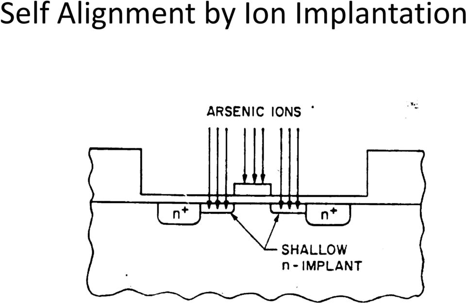
9 Self Alignment by Ion Implantation
10 Metallization IC metallization provides the ohmic contact with the semiconductor Multilayer constructions are often required due to adhesion requirement. Adhesion layers include Ti,Ti/W, Cr, Co Multi-level interconnects required for on-chip interconnection. 2-5 layers currently Metallizations must be capable of fine line fabrication ( currently.25 microns) and must be resistant to hillock formation, electromigration, etc) Size reduction increases need for high conductivity

11 Multilayer IC Metallization

12 SIA Roadmap for Chip Interconnections

13 SEM View of Multilayer IC Metallization

14 Passive Components Capacitors Ceramic Tantalum solid electrolytic aluminum electrolytic Resistors thick film chip power Magnetic devices inductors transformers

15 Recent changes Affecting Passive Components DOD Acquisition reform; abandonment of military specifications and associated audit and quality control functions World wide ISO9000 quality standards, increasing offshore competition Drive towards miniaturization, low power, high frequency applications Increases in automotive, communication and computer applications

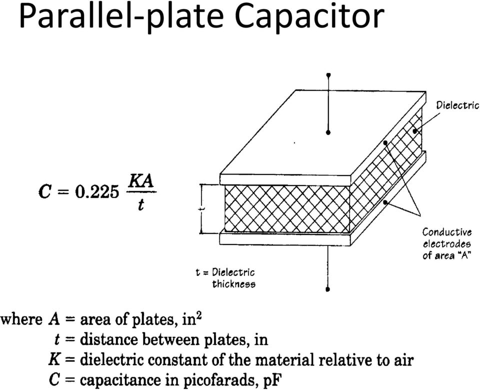
16 Parallel-plate Capacitor
17 Capacitor Properties Capacitance and tolerance Voltage rating Equivalent series resistance(esr) and power loss Insulating resistance (leakage current) AC rating Capacitance stability with temperature and frequency

18 Principle Capacitor Types Ceramic chip capacitor dielectrics made from sintered ceramics, often barium titanate most widely used style: low cost, wide range of characteristics, small size, excellent high frequency properties Solid electrolyte tantalum capacitors high volumetric efficiency, good stability and high reliability leakage current, limited voltage range and polarity can be problems Aluminum electrolytic Metallized plastic capacitors

19 Ceramic Chip Capacitor Construction Consists of an inter-digitated set of ceramic dielectric layers with metal electrodes Dielectric is based on high K ferroelectric barium titanate (BaTiO 3 ) or paraelectric titanates for NPO dielectrics Electrodes are Ag or Ag/Pd alloys End terminations are thick film metallizations, which can be Ni plated to minimize solder leaching Value within a size range obtained by increasing the number of layers, as the dielectric thickness remains constant

20 Typical Ceramic Chip Capacitor Construction End Termination

21 Dielectric Properties
22 Deaging After undergoing the phase transformation at the Curie temperature, the effective dielectric constant will decrease with time due to domain relaxation. This is called deaging. For BX dielectrics, it is about 2%/decade hr. NPO does not deage because it is fabricated from a paraelectric dielectric
23 Barium Titanate Crystal Structure Cubic Perovskite Structure Tetragonal Structure Below the Curie Point
24 Temperature Coefficient of Capacitance The temperature response of BaTiO 3 can be modified by either adding materials that shift the Curie point (usually solid solutions perovskites) or suppress the dielectric response over temperature (depressors). Shifters Depressors
25 Size Configuration Size configuration ranges from 0402 to 2225, with 0201 currently being introduced. Due to size reduction constraints, the smaller sizes are preferred.the choice of dielectric (NPO, X7R, Z5U) allows a wide range of values to be obtained, based on electrical and reliability performance.
26 Tantalum Electrolytic Capacitors Solid electrolytic tantalum capacitors have the highest vales of capacitance per size for chip components The high capacitance is obtained by using a large area ( porous sintered powder) and a thin dielectric thickness ( tantalum oxide from 10 to 70 nanometers(.01 µm) The capacitors are polar-i.e. they have a positive and negative terminal and circuit polarity must be observed. Reverse operation can lead to dielectric breakdown and catastrophic failure
27 Solid Tantalum Electrolytic Capacitor Tantalum capacitor has an porous sintered tantalum anode body with an electrochemically formed tantalum oxide dielectric. The counter-electrode is made from a semiconducting film of manganese dioxide and colloidal graphite/silver epoxy coating
28 SMT Configurations for Tantalum Capacitors Molder SMT Configuration Hybrid tantalum chip capacitor
29 Sizes of Tantalum Capacitors per MIL-C For a given size, the value is changed by the thickness of the dielectric, and hence the voltage rating. Thus in size A, capacitors from the range 0.1 to 2.2 microfarads are available
30 Resistor Properties Resistance and tolerance Stability during operation Resistance stability with temperature and voltage Maximum working voltage Critical resistance value for a given voltage and power rating, the resistance value that would dissipate full rated power at rated voltage Noise
31 Chip Resistors Chip resistors are typically thick film resistors on an alumina substrate with wrap around end terminations or standard thick film inks ( Pd-Ag) Chip resistors come in the size configuration of chip capacitors, however, a single size covers all values and is determined by power. For size constrained applications, small sizes, such as 0504 or smaller, are utilized Chip resistors are also available in thin film, with lower TCRs, and in arrays.
32
33
34 Chip Resistor
35 MELF Construction Metal Electrode face bonding (MELF) are a packaging configuration which is used for circular devices ( or devices which were previously leaded, with a circular body. This includes diodes, resistors, and capacitors
36 Magnetic Devices Classified by construction and use: Coil: conductor wound in helical or spherical shape to form an inductor Choke: simple coil that conducts DC, but impedes ac current due to inductance Core: magnetizable portion of a device Transformer: two inductively coupled wirewound coils, usually on a single core. Used to step-up or step-down voltage at the same ac frequency
37 Magnetic Properties DC resistance Inductance Permeability Quality factor: ratio of stored to dissipated energy per cycle Self resonant frequency Temperature rating Voltage rating, insulation resistance
38 Chip Inductor Cross-sectional view
39 Other Components Crystals, crystal oscillators Connectors Switches Fuses Relays
40 Application Considerations Derating Environmental Stresses temperature mechanical humidity EMI/RF others Attachment procedures Circuit considerations
41 Derating Operating components at electrical and environmental stress levels lower than the maximum rated to reduce failure rates Recommended factors ( fraction of maximum rated stress to be used) vary with part type, materials, and quality levels Summary table just supplies general information: detailed information needed for specific application
42 Derating Factors, Summary Part Derating Factor Stress Diodes Current, PIV Transistors 0.5 Power, Current ICs 0.8 Current, Voltage, Power Capacitor Voltage Resistor 0.5 Power Feedthru filters 0.7 Voltage,Current Switches 0.8 Current Transformers 0.4 Power Fuses 0.5 Output current
43 Packaging Trends Wider use of Multichip Modules (MCM) and multichip Packages (MCP) MCP s will have same footprint as single chip packages Migration from Perimeter I/O to area I/O Single chip package will migrate smaller to chip scale IC s will continue to follow Rent s Rule, with increases in I/O and memory doubling every 2.5 years
44 SAI Roadmap for ICs (1995)
45 SAI Roadmap
46 Packaging Trends
47 Component Density for Portable Electronics
48 First Level Assembly First level assembly interconnects the component to the next higher level of assembly, either a discrete package or directly to the interconnect structure as in direct chip attach (DCA) techniques First level attach includes ultrasonic aluminum and thermosonic gold wire bonding,tab (tape automated bonding) and soldering
49 Wire Bonding for First Level Interconnection
50 Aluminum Ultrasonic Wedge Bonding The aluminum wire (typically 1 mil, but ranges from.7 to 10 mils)is located between the tool and the material to be bonded The tool presses against the surface at a predetermined force and ultrasonic energy is applied in a lateral motion The tool is raised while the wire is played out from the spool The tool is placed over the second bond location, brought into contact and pressure and ultrasonic energy is applied A wire clamp closes and pulls on the wire, breaking it at the heel of the bond
51 Aluminum Ultrasonic Wedge Bonding
52 Al Wedge Bonding (Cont.)
53 Gold Thermosonic Ball Bonding Gold wire is feed through the capillary, and a electric discharge melts the wire into a ball at the tip The ball is positioned against the bottom of the capillary, lowered to the bonding pad on the device to be bonded, which is heated. Ultrasonic energy and pressure are applied The tool is raised with the wire able to slip through the capillary. The tool is positioned over the second bond The tool is lowered to produce the second bond (called a stitch bond) The tool is raised while the wire is clamped, causing the wire to break
54 Top and Side View of a Wedge Bond
55 Gold Thermosonic Ball Bonding
56 Gold Thermosonic Ball Bonding (Cont.)
57 Top and Side View of a Ball Bond
58 Gold Ball Bonds First bond Second bond
59 Ultrasonic Wedge Bonds First Bond Second bond
60 Spacing Limitations for Ball Bonding
61 Wire Bond Examples Staggered Bonds to Reduce Effective Pitch Examples of Fine-pitch Ball and Wedge Bonds
62 Tape Automated Bonding TAB was developed to allow simultaneous bonding of all chip bonds ( inner lead bonds) by thermocompression bonding TAB requires a gold bump on either the chip or the lead for the inner lead bond (ILB) The outer lead bond (OLB) is usually soldered but can be thermosonically bonded
63 TAB Construction, Prior to Excising the Chip
64 TAB Inner Lead Bonding
65 Bumping Options for TAB Bumped Chip Bumped Tape
66 Gold Bump Process
67 40 Lead Tab Tape Example Mesa Technology
68 Solder Assembly Another method of first level assembly is to create solder balls at the IC pad locations. Since solder does not wet aluminum, a multilayer metallization structure must be provided to provide adhesion and leach resistance ( example Cr, Ti, Ti-W) and easy wetting for the solder (Cu, Ni, Au) Solder could be added by plating or evaporation through a mask,
69 Flip Chip Assembly
70 Solder Bumping
71 Solder Bump
72 Solder Bump Metallizations Hitachi Honeywell-Bull
73 Single Chip Packaging Through Hole Packages Surface Mounted Packages
74 Molded Plastic Packages
75 Types of First Level Packages
76
77
78
79 Through Hole Versus Surface Mount Assembly Technique Surface Mount Technology Through Hole Technology
80 Comparison of SMT and Thru-hole Component Sizes Passive Components Active Components
81 Ball Grid Array Packages
82 QFP-PBGA Size Comparison A comparison of the 208 lead QFP and the 208 lead PBGA demonstrates the size reduction in moving from peripheral to area array connections
83 High I/O Packages (PQFP/BGAs) PQFP are projected to dominate I/O counts up to 200, with 0.5mm lead pitch BGAs will dominate over 300 I/Os, due to small pitch (0.3mm) of equivalent PQFPs and area efficiencies of BGAs Although BGAs are projected to grow at 25%/year, only 2 billion BGAs are anticipated in use by 2004, compared to 23 billion PQFPs BGA availability up to 736 I/Os (TBGA)
84 BGA Formats Plastic overmolded (PBGA)-up to 400I/O Tape carrier (TBGA) -up to 736 I/O Ceramic (CBGA)-up to 625 I/O Ceramic Column (CCBGA)- over 1000 I/O Cavity BGA-up to 596 I/O Metal body (MBGA)
85 Plastic BGA
86 Plastic Ball Grid Array (PBGA)Package PWB laminate substrate, usually BT or similar Wire bonded or flip chip Cavity up or down Bulk of body is molding compound; can be combined with a heat sink.030 diameter solder balls, usually eutectic or Sn62 Typically 1.27 or 1.5 mm grid, mm body size Multiple manufactures ( Amkor, Motorola, IBM,
87 Ceramic Ball Grid Array (CBGA) Package Standard multilayer ceramic substrate Flip chip or wire bonded White or black ceramic Cavity up or down /10 Pb/Sn solder balls Typically 1.27 mm grid, 18 to 32 mm body size Balls attached with eutectic solder
88 CBGA
89 Tape Ball Grid Array (TBGA) Packages 2 metal layer( 1 ground, I signal) TAB type substrate Flip chip or TAB bonding 25 mil diameter 90/10 Pb/Sn solder balls. Balls attached by partial reflow to plated through holes of the TAB substrate A stiffner is attached to the outer-lead portion of the substrate. The entire package is epoxy encapsulated
90 TBGA
91 Various Ball Configurations
92 Chip Scale Packages (CSP) Currently over 50 CSP packages are available as: leadframe-based rigid substrate-based (PWB or ceramic) wafer level flex-circuit-based Flex producers can handle design rules of less than 65 µm pitch, allowing single metal layer routing
93 CSP Configurations
94 Tessera Compliant Chip CSP
95 Peripheral-Area Fan-in for Tessera µbga
96 Slightly Larger than IC (SLICC) Package
97 Tape Based CSPs Tape based CSP are the µbga (Tessera) and the flexbga µbga uses a face down die interconnected via TAB construction. Typically a fan-in approach flexbga is a fan-in/out technology. It is a face-up, flexbga is a fan-in/out technology. It is a face-up, wire bonded, overmolded structure on a single layer polyimide tape, similar to TAB tape
98 Ceramic CSP Multilayer alumina carrier with gold stud bumped die, mounted with conductive adhesive Matsushita
99 Die Size CSP (Shellcase)
100 Different CSP Constructions
101 Progression of Package Types
102 Package on Package (POP)
103 Stacked Die in Package
104 Multi-die in Package
105 Flex Stacked die Package
106 Comparison of µbga Versus Flip Chip
107 Underfilling Flip Chip
108 Underfill Encapsulants Provides strain relief for bumped solder connects by averaging load over entire layer, not only the bumps Must achieve low CTE with extremely low viscosities and high flow Dispensed along the edge of a preheated board to maximize flow Capillary action draws underfill under the chip Underfills are chemically tailored for the substrate material to accommodate different surface tensions
109 Effect of Underfill Prior to the introduction of underfilling, flip chip assembly on organic boards failed in thermal cycle after a few tens of cycles Using underfill, the same construction can survive over 5000 thermal cycles Underfill will allow flip chip DCA to become a dominant assembly method Underfill developments include methods where the encapsulant is applied prior to chip attach to minimize manufacturing time
110 Effect of Underfill on Temp Cycling Performance With filler, 27ppm
111 Reflow Encapsulation Underfill is applied prior to soldering Acts as adhesive prior to reflow Acts as a flux during soldering ( no clean) Cures as an encapsulant/underfill on exposure to the soldering temperature Minimizes post soldering operations
112 Kester Reflow Encapsulant
113 I/O Redistribution Type of Wafer-level CSP
114 Ball Formation- Electroplate Method
115 Paste Method for Ball Formation
116 Multi-chip CSP
117 Glob-top/Dam and Fill Encapsulation For direct chip attach, environmental protection must be provides Glob-top is the oldest,method to protect wirebonds, with controlled flow that allowed penetration between the wires and overmolding of the die in one step For fine pitch requirements, a more fluid encapsulation is desired to insure penetration of the wire bonds. In dam and fill, a dam is formed from a highly thixotropic encapsulant, followed by a fill of the highest possible flow encapsulant
118 Dam and Fill
119 SLC Process
120 Surface Laminar Circuit -SLC
121 Embedded Passives LTCC provides great promise for maximum product density with the ability to embed passive components within the LTCC substrate Currently, resistor, capacitors and inductors Currently, resistor, capacitors and inductors can be buried because of the materials compatibility of thick film materials and the multilayer construction
122 LTCC with Buried Components
1.Introduction. Introduction. Most of slides come from Semiconductor Manufacturing Technology by Michael Quirk and Julian Serda.
 .Introduction If the automobile had followed the same development cycle as the computer, a Rolls- Royce would today cost $00, get one million miles to the gallon and explode once a year Most of slides
 Preface xiii Introduction xv 1 Planning for surface mount design General electronic products 3 Dedicated service electronic products 3 High-reliability electronic products 4 Defining the environmental
Ball Grid Array (BGA) Technology
 Technology") Chapter E: BGA Ball Grid Array (BGA) Technology The information presented in this chapter has been collected from a number of sources describing BGA activities, both nationally at IVF and reported elsewhere
Chapter E: BGA Ball Grid Array (BGA) Technology The information presented in this chapter has been collected from a number of sources describing BGA activities, both nationally at IVF and reported elsewhere
DESIGN GUIDELINES FOR LTCC
 DESIGN GUIDELINES FOR LTCC HERALOCK HL2000 MATERIALS SYSTEM Preliminary Guideline Release 1.0 CONTENTS 1. INTRODUCTION 1.1. GLOSSARY OF TERMS 1.2. LTCC PROCESS FLOW DIAGRAM 1.3. UNITS OF MEASURE 2. PROCESSING
Flip Chip Package Qualification of RF-IC Packages
 Flip Chip Package Qualification of RF-IC Packages Mumtaz Y. Bora Peregrine Semiconductor San Diego, Ca. 92121 mbora@psemi.com Abstract Quad Flat Pack No Leads (QFNs) are thermally enhanced plastic packages
CIRCUITS AND SYSTEMS- Assembly and Printed Circuit Board (PCB) Package Mohammad S. Sharawi ASSEMBLY AND PRINTED CIRCUIT BOARD (PCB) PACKAGE
 Package Mohammad S. Sharawi ASSEMBLY AND PRINTED CIRCUIT BOARD (PCB) PACKAGE") ASSEMBLY AND PRINTED CIRCUIT BOARD (PCB) PACKAGE Mohammad S. Sharawi Electrical Engineering Department, King Fahd University of Petroleum and Minerals Dhahran, 31261 Saudi Arabia Keywords: Printed Circuit
ASSEMBLY AND PRINTED CIRCUIT BOARD (PCB) PACKAGE Mohammad S. Sharawi Electrical Engineering Department, King Fahd University of Petroleum and Minerals Dhahran, 31261 Saudi Arabia Keywords: Printed Circuit
A Manufacturing Technology Perspective of: Embedded Die in Substrate and Panel Based Fan-Out Packages
 A Manufacturing Technology Perspective of: Embedded Die in Substrate and Panel Based Fan-Out Packages Bernd K Appelt Director WW Business Development April 24, 2012 Table of Content Definitions Wafer Level
Fraunhofer ISIT, Itzehoe 14. Juni 2005. Fraunhofer Institut Siliziumtechnologie (ISIT)
") Research and Development centre for Microelectronics and Microsystems Applied Research, Development and Production for Industry ISIT applies an ISO 9001:2000 certified quality management system. Certificate
Research and Development centre for Microelectronics and Microsystems Applied Research, Development and Production for Industry ISIT applies an ISO 9001:2000 certified quality management system. Certificate
Designing with High-Density BGA Packages for Altera Devices
 2014.12.15 Designing with High-Density BGA Packages for Altera Devices AN-114 Subscribe As programmable logic devices (PLDs) increase in density and I/O pins, the demand for small packages and diverse
Dual Integration - Verschmelzung von Wafer und Panel Level Technologien
 ERÖFFNUNG DES INNOVATIONSZENTRUMS ADAPTSYS Dual Integration - Verschmelzung von Wafer und Panel Level Technologien Dr. Michael Töpper BDT Introduction Introduction Why do we need such large machines to
Miniaturizing Flexible Circuits for use in Medical Electronics. Nate Kreutter 3M
 Miniaturizing Flexible Circuits for use in Medical Electronics Nate Kreutter 3M Drivers for Medical Miniaturization Market Drivers for Increased use of Medical Electronics Aging Population Early Detection
Axial and Radial Leaded Multilayer Ceramic Capacitors for Automotive Applications Class 1 and Class 2, 50 V DC, 100 V DC and 200 V DC
 Axial and Radial Leaded Multilayer Ceramic Capacitors for Automotive Applications Class 1 and Class 2, 5 V DC, 1 V DC and 2 V DC DESIGNING For more than 2 years Vitramon has supported the automotive industry
Specializing in Open Cavity Packages & Complete IC Assembly Services ISO 9001:2008 Certified and ITAR Registered
 TowerJazz Global Symposium Specializing in Open Cavity Packages & Complete IC Assembly Services and TowerJazz Global Symposium Quik-Pak a division of Delphon Industries 2011 Gold Sponsor and TowerJazz
Guide for Molded Tantalum Capacitors
 Guide for Molded Tantalum Capacitors INTRODUCTION Tantalum electrolytic capacitors are the preferred choice in applications where volumetric efficiency, stable electrical parameters, high reliability,
Copyright 2008 IEEE. Reprinted from ECTC2008 Proceedings.
 Copyright 2008 IEEE. Reprinted from ECTC2008 Proceedings. This material is posted here with permission of the IEEE. Such permission of the IEEE does not in any way imply IEEE endorsement of any of Amkor
NBB-402. RoHS Compliant & Pb-Free Product. Typical Applications
 Typical Applications Narrow and Broadband Commercial and Military Radio Designs Linear and Saturated Amplifiers 0 RoHS Compliant & Pb-Free Product NBB-402 CASCADABLE BROADBAND GaAs MMIC AMPLIFIER DC TO
What is surface mount?
 A way of attaching electronic components to a printed circuit board The solder joint forms the mechanical and electrical connection What is surface mount? Bonding of the solder joint is to the surface
Flexible Printed Circuits Design Guide
 www.tech-etch.com/flex Flexible Printed Circuits Design Guide Multilayer SMT Assembly Selective Plating of Gold & Tin-Lead Fine Line Microvias Cantilevered & Windowed Leads 1 MATERIALS CONDUCTOR Copper
Investigation of Components Attachment onto Low Temperature Flex Circuit
 Investigation of Components Attachment onto Low Temperature Flex Circuit July 2013 Q. Chu, N. Ghalib, H. Ly Agenda Introduction to MIRA Initiative MIRA Manufacturing Platforms Areas of Development Multiphase
Lecture 030 DSM CMOS Technology (3/24/10) Page 030-1
 Page 030-1") Lecture 030 DSM CMOS Technology (3/24/10) Page 030-1 LECTURE 030 - DEEP SUBMICRON (DSM) CMOS TECHNOLOGY LECTURE ORGANIZATION Outline Characteristics of a deep submicron CMOS technology Typical deep submicron
Lecture 030 DSM CMOS Technology (3/24/10) Page 030-1 LECTURE 030 - DEEP SUBMICRON (DSM) CMOS TECHNOLOGY LECTURE ORGANIZATION Outline Characteristics of a deep submicron CMOS technology Typical deep submicron
High Density SMT Assemblies Based on Flex Substrates
 High Density SMT Assemblies Based on Flex Substrates Robert Larmouth, James Keating Teledyne Electronic Technologies 110 Lowell Rd., Hudson, NH 03051 (603) 889-6191 Abstract The industry trend to shrink
POWER FORUM, BOLOGNA 20-09-2012
 POWER FORUM, BOLOGNA 20-09-2012 Convertitori DC/DC ad alta densità di potenza e bassa impedenza termica. Massimo GAVIOLI. Senior Field Application Engineer. Intersil SIMPLY SMARTER Challenges when Designing
(11) PCB fabrication / (2) Focused assembly
 PCB fabrication / (2) Focused assembly") Company Fact Sheet TTM Technologies, Inc. is a world-wide leader in the manufacture of technologically advanced PCBs, backplane and sub-system assemblies. Our Global Presence / Local Knowledge approach
Company Fact Sheet TTM Technologies, Inc. is a world-wide leader in the manufacture of technologically advanced PCBs, backplane and sub-system assemblies. Our Global Presence / Local Knowledge approach
GaN IC Die Handling, Assembly and Testing Techniques
 GaN IC Die Handling, Assembly and Testing Techniques Page 1 of 9 1. Scope This document describes the storage and handling requirements for GaN IC chips. It also describes recommended assembly and testing
Good Boards = Results
 Section 2: Printed Circuit Board Fabrication & Solderability Good Boards = Results Board fabrication is one aspect of the electronics production industry that SMT assembly engineers often know little about.
INEMI 2007 Roadmap Organic Substrates. Jack Fisher, Interconnect Technology Analysis, Inc. Celestica-iNEMI Technology Forum May 15, 2007
 INEMI 2007 Roadmap Organic Substrates Jack Fisher, Interconnect Technology Analysis, Inc. Celestica-iNEMI Technology Forum May 15, 2007 Introduction The interconnecting substrates functional role provides
Chip-on-board Technology
 Hybrid Technology The trend in electronics is to continue to integrate more and more functions and numbers of components into a single, smaller assembly. Hybrid circuit technology is a key method of increasing
Chapter 10 Circuit Manufacture
 RF Electronics Chapter 10: Circuit Manufacture Page 1 Introduction Chapter 10 Circuit Manufacture Printed Circuits Boards consist of an insulating material forming the PCB substrate onto which conductive
WW12X, WW08X, WW06X, WW04X ±1%, ±5% Thick Film Low ohm chip resistors
 WW12X, WW08X, WW06X, WW04X ±1%, ±5% Thick Film Low ohm chip resistors Size 1206, 0805, 0603, 0402 *Contents in this sheet are subject to change without prior notice. Page 1 of 8 ASC_WWxxX_V12 Nov.- 2011
COPPER FLEX PRODUCTS
 COPPER FLEX PRODUCTS WHY FLEX? Molex ible Printed Circuit Technology is the answer to your most challenging interconnect applications. We are your total solution for ible Printed Circuitry because we design
Webinar HDI Microvia Technology Cost Aspects
 Webinar HDI Microvia Technology Cost Aspects www.we-online.com HDI - Cost Aspects Seite 1 1 July, 2014 Agenda - Webinar HDI Microvia Technology Cost Aspects Reasons for the use of HDI technology Printed
2.996/6.971 Biomedical Devices Design Laboratory Lecture 2: Fundamentals and PCB Layout
 2.996/6.971 Biomedical Devices Design Laboratory Lecture 2: Fundamentals and PCB Layout Instructor: Hong Ma Sept. 12, 2007 Fundamental Elements Resistor (R) Capacitor (C) Inductor (L) Voltage Source Current
Embedding components within PCB substrates
 Embedding components within PCB substrates Max Clemons, Altium - March 19, 2014 Continued pressure for electronic devices that provide greater functionality in ever-smaller formfactors is not only providing
Integrated Circuit Packaging and Thermal Design
 Lezioni di Tecnologie e Materiali per l Elettronica Integrated Circuit Packaging and Thermal Design Danilo Manstretta microlab.unipv.it danilo.manstretta@unipv.it Introduction to IC Technologies Packaging
Introduction to VLSI Fabrication Technologies. Emanuele Baravelli
 Introduction to VLSI Fabrication Technologies Emanuele Baravelli 27/09/2005 Organization Materials Used in VLSI Fabrication VLSI Fabrication Technologies Overview of Fabrication Methods Device simulation
Xilinx Advanced Packaging
 Xilinx Advanced Packaging Electronic packages are the interconnect housings for semiconductor devices. They provide electrical interconnections between the IC and the board, and they efficiently remove
Polymer Termination. Mechanical Cracking 2. The reason for polymer termination. What is Polymer Termination? 3
 Polymer Termination An alternative termination material specifically designed to absorb greater levels of mechanical stress thereby reducing capacitor failures associated with mechanical cracking Mechanical
0.08 to 0.31 mils. IC Metal Interconnect. 6 mils. Bond Wire. Metal Package Lead Frame. 40 mils. PC Board. Metal Trace on PC Board 18507
 3 PACKAGING Packaging the IC chip is a necessary step in the manufacturing process because the IC chips are small, fragile, susceptible to environmental damage, and too difficult to handle by the IC users.
Printed Circuits. Danilo Manstretta. microlab.unipv.it/ danilo.manstretta@unipv.it. AA 2012/2013 Lezioni di Tecnologie e Materiali per l Elettronica
 Lezioni di Tecnologie e Materiali per l Elettronica Printed Circuits Danilo Manstretta microlab.unipv.it/ danilo.manstretta@unipv.it Printed Circuits Printed Circuits Materials Technological steps Production
Microstockage d énergie Les dernières avancées. S. Martin (CEA-LITEN / LCMS Grenoble)
") Microstockage d énergie Les dernières avancées S. Martin (CEA-LITEN / LCMS Grenoble) 1 Outline What is a microbattery? Microbatteries developped at CEA Description Performances Integration and Demonstrations
Microstockage d énergie Les dernières avancées S. Martin (CEA-LITEN / LCMS Grenoble) 1 Outline What is a microbattery? Microbatteries developped at CEA Description Performances Integration and Demonstrations
Adapters - Overview. Quick-Turn Solutions for IC Supply Issues
 Adapters - Overview BGA to BGA Adapter BGA to PGA BGA to QFP BGA to BGA QFP to BGA SMT to DIP SMT to SMT PGA to PGA BGA to QFP Adapter with VR using FlexFrame Interconnect TSOP Adapter Packaged Die to
Accelerated Thermal Cycling and Failure Mechanisms For BGA and CSP Assemblies
 Accelerated Thermal Cycling and Failure Mechanisms For BGA and CSP Assemblies Reza Ghaffarian, Ph.D. Jet Propulsion Laboratory California Institute of Technology Pasadena, California 818-354-2059 reza.ghaffarian@jpl.nasa.gov
HDI. HDI = High Density Interconnect. Kenneth Jonsson Bo Andersson. NCAB Group
 HDI HDI = High Density Interconnect Kenneth Jonsson Bo Andersson NCAB Group Definitions / Standards (IPC) Pros & Cons Key equipment Build-ups Choice of material Design rules IPC HDI reliability (µvia stacked
Flex Circuit Design and Manufacture.
 Flex Circuit Design and Manufacture. Hawarden Industrial Park, Manor Lane, Deeside, Flintshire, CH5 3QZ Tel 01244 520510 Fax 01244 520721 Sales@merlincircuit.co.uk www.merlincircuit.co.uk Flex Circuit
Multilevel Socket Technologies
 Multilevel Socket Technologies High Performance IC Sockets And Test Adapters Overview Company Overview Over 5,000 products High Performance Adapters and Sockets Many Custom Designs & Turn-Key Solutions
Winbond W2E512/W27E257 EEPROM
 Construction Analysis Winbond W2E512/W27E257 EEPROM Report Number: SCA 9703-533 Global Semiconductor Industry the Serving Since 1964 15022 N. 75th Street Scottsdale, AZ 85260-2476 Phone: 602-998-9780 Fax:
Electronic Board Assembly
 Electronic Board Assembly ERNI Systems Technology Systems Solutions - a one stop shop - www.erni.com Contents ERNI Systems Technology Soldering Technologies SMT soldering THR soldering THT soldering -
MADP-000504-10720T. Non Magnetic MELF PIN Diode
 MADP-54-172T Features High Power Handling Low Loss / Low Distortion Leadless Low Inductance MELF Package Non-Magnetic Surface Mountable RoHS Compliant MSL 1 Package Style 172 Dot Denotes Cathode Description
INTERNATIONAL ATOMIC ENERGY AGENCY INSTRUMENTATION UNIT SMD (SURFACE MOUNTED DEVICES) REPAIR S. WIERZBINSKI FEBRUARY 1999
 REPAIR S. WIERZBINSKI FEBRUARY 1999") (SURFACE MOUNTED DEVICES) REPAIR S. WIERZBINSKI FEBRUARY 1999 (SURFACE MOUNTED DEVICES) REPAIR 1 TABLE OF CONTENTS PAGE 1. INTRODUCTION 3 2. ADVANTAGES 4 3. LIMITATIONS 4 4. DIALECT 5 5. SIZES AND DIMENSIONS
(SURFACE MOUNTED DEVICES) REPAIR S. WIERZBINSKI FEBRUARY 1999 (SURFACE MOUNTED DEVICES) REPAIR 1 TABLE OF CONTENTS PAGE 1. INTRODUCTION 3 2. ADVANTAGES 4 3. LIMITATIONS 4 4. DIALECT 5 5. SIZES AND DIMENSIONS
Molded. By July. A chip scale. and Omega. Guidelines. layer on the silicon chip. of mold. aluminum or. Bottom view. Rev. 1.
 Application Note PAC-006 By J. Lu, Y. Ding, S. Liu, J. Gong, C. Yue July 2012 Molded Chip Scale Package Assembly Guidelines Introduction to Molded Chip Scale Package A chip scale package (CSP) has direct
Pulse Withstanding Thick Film Chip Resistor-SMDP Series. official distributor of
 Product: Pulse Withstanding Thick Film Chip Resistor-SMDP Series Size: /// official distributor of Pulse Withstanding Thick Film Chip Resistor-SMDP Series 1. Scope -This specification applies to ~ sizes
Module No. # 06 Lecture No. # 31 Conventional Vs HDI Technologies Flexible Circuits Tutorial Session
 An Introduction to Electronics Systems Packaging Prof. G. V. Mahesh Department of Electronic Systems Engineering Indian Institute of Science, Bangalore Module No. # 06 Lecture No. # 31 Conventional Vs
Power Dissipation Considerations in High Precision Vishay Sfernice Thin Film Chips Resistors and Arrays (P, PRA etc.) (High Temperature Applications)
 (High Temperature Applications)") VISHAY SFERNICE Resistive Products Application Note ABSTRACT On our thin film chips resistors and arrays the main path for the heat, more than 90 %, is conduction through the body of the component, the
VISHAY SFERNICE Resistive Products Application Note ABSTRACT On our thin film chips resistors and arrays the main path for the heat, more than 90 %, is conduction through the body of the component, the
Rogers 3003, 3006, 3010, 3035, 3203, 3206, 3210
 Stocked Materials: RIGID STANDARD FR4 High Tg 170c Black FR4 Polyclad 370HR (Lead Free) HIGH RELIABILITY Polyimide (Arlon 85N, Isola P96) BT (G200) HIGH FREQUENCY: Park Nelco 4000-13, 4000-13si Getek Gore
MMIC packaging. 1. Introduction 2. Data interface. Data submittal methods. Data formats. Single chip & MCM solutions. Contents
 MMIC packaging MMIC packaging Contents 1. Introduction Page 2 2. Data Interface Page 2 3. Microwave package design requirement Page 3 4. Materials Page 3 5. Package layout design guidelines Page 4 6. Package
Advanced VLSI Design CMOS Processing Technology
 Isolation of transistors, i.e., their source and drains, from other transistors is needed to reduce electrical interactions between them. For technologies
TC50 High Precision Power Thin Film chip resistors (RoHS compliant Halogen Free) Size 1206, 0805, 0603
 Size 1206, 0805, 0603") WF2Q, WF08Q, WF06Q ±%, ±0.5%, ±0.25%, ±0.%, ±0.05% TC50 High Precision Power Thin Film chip resistors (RoHS compliant Halogen Free) Size 206, 0805, 0603 *Contents in this sheet are subject to change without
WF2Q, WF08Q, WF06Q ±%, ±0.5%, ±0.25%, ±0.%, ±0.05% TC50 High Precision Power Thin Film chip resistors (RoHS compliant Halogen Free) Size 206, 0805, 0603 *Contents in this sheet are subject to change without
DRIVING COST OUT OF YOUR DESIGNS THROUGH YOUR PCB FABRICATOR S EYES!
 4/3/2013 S THROUGH YOUR PCB FABRICATOR S EYES! Brett McCoy Eagle Electronics Schaumburg IL. New England Design and Manufacturing Tech Conference Brett McCoy: Vice President / Director of Sales Circuit
Thermal Adhesives Ther-O-Bond 1500
 Products / Interface Materials / Adhesives Adhesives Bond 1500 Epoxy casting system for potting and encapsulation Bond 1600 Two part epoxy for bonding Bond 2000 Rapid cure acrylic adhesive bond High strength
Surface Mount Multilayer Ceramic Chip Capacitor Solutions for High Voltage Applications
 Surface Mount Multilayer Ceramic Chip Capacitor Solutions for High Voltage Applications ELECTRICAL SPECIFICATIONS X7R GENERAL SPECIFICATION Note Electrical characteristics at +25 C unless otherwise specified
Global Semiconductor Packaging Materials Outlook
 NOVEMBER 2009 Global Semiconductor Packaging Materials Outlook Produced by Semiconductor Equipment and Materials International and TechSearch International, Inc. EXECUTIVE SUMMARY 1 1 INTRODUCTION 5 1.1
Bi-directional FlipFET TM MOSFETs for Cell Phone Battery Protection Circuits
 Bi-directional FlipFET TM MOSFETs for Cell Phone Battery Protection Circuits As presented at PCIM 2001 Authors: *Mark Pavier, *Hazel Schofield, *Tim Sammon, **Aram Arzumanyan, **Ritu Sodhi, **Dan Kinzer
Powering Integrated Circuits (ICs), and managing ripple voltage as it relates
, and managing ripple voltage as it relates") Ripple Voltage & ESR Powering Integrated Circuits (ICs), and managing ripple voltage as it relates to ESR of capacitors Low voltage ICs require supply voltage (Vcc) to have reduced levels of ripple voltage
Ripple Voltage & ESR Powering Integrated Circuits (ICs), and managing ripple voltage as it relates to ESR of capacitors Low voltage ICs require supply voltage (Vcc) to have reduced levels of ripple voltage
IBS - Ion Beam Services
 IBS - Ion Beam Services Profile Technologies Devices & sensor fabricat ion Participation to R&D programs Researched partnership Présentation activité composant 1 Profile : Products and services Product
Bourns Resistive Products
 Bourns Resistive Products Diverse Requirements Drive Innovations to Pulse Resistors Introduction Countless circuits depend on the protection provided by one of the most fundamental types of passive components:
White Paper. Recommendations for Installing Flash LEDs on Flex Circuits. By Shereen Lim. Abstract. What is a Flex Circuit?
 Recommendations for Installing Flash LEDs on Circuits By Shereen Lim White Paper Abstract For the mobile market some PCB assemblies have been converted to flex circuit assemblies, in part because flex
How to Avoid Conductive Anodic Filaments (CAF)
") How to Avoid Conductive Anodic Filaments (CAF) Ling Zou & Chris Hunt 22 January 20 1 Your Delegate Webinar Control Panel Open and close your panel Full screen view Raise hand for Q&A at the end Submit
How to Avoid Conductive Anodic Filaments (CAF) Ling Zou & Chris Hunt 22 January 20 1 Your Delegate Webinar Control Panel Open and close your panel Full screen view Raise hand for Q&A at the end Submit
FABRICATION 2011 SERVICES TECHNOLOGIES CAPABILITIES INDUSTRY
 FABRICATION 2011 SERVICES 24HRS - 5 DAYS ON QUICK TURN PROTOTYPE Dear Customer, We would like to take this opportunity to welcome you and thank you for looking to ASA PCB as your Printed Circuit Manufacturing
Dry Film Photoresist & Material Solutions for 3D/TSV
 Dry Film Photoresist & Material Solutions for 3D/TSV Agenda Digital Consumer Market Trends Components and Devices 3D Integration Approaches Examples of TSV Applications Image Sensor and Memory Via Last
How to Build a Printed Circuit Board. Advanced Circuits Inc 2004
 How to Build a Printed Circuit Board 1 This presentation is a work in progress. As methods and processes change it will be updated accordingly. It is intended only as an introduction to the production
Type RP73 Series. SMD High Power Precision Resistors. Key Features. Applications. Characteristics - Electrical - RP73 Series - Standard
 Key Features n High precision - tolerances down to 0.05% n Low TCR - down to 5ppm/ C n Stable high frequency performance n Operating temperature -55 C to +155 C n Increased power rating - up to 1.0W n
ENIG with Ductile Electroless Nickel for Flex Circuit Applications
 ENIG with Ductile Electroless Nickel for Flex Circuit Applications Yukinori Oda, Tsuyoshi Maeda, Chika Kawai, Masayuki Kiso, Shigeo Hashimoto C.Uyemura & Co., Ltd. George Milad and Donald Gudeczauskas
Fabrication of Embedded Capacitance Printed Circuit Boards
 Presented at IPC Printed Circuits EXPO 2001 www.ipcprintedcircuitexpo.org Fabrication of Embedded Capacitance Printed Circuit Boards Joel S. Peiffer 3M St. Paul, MN Abstract Embedding capacitor materials
PCB Assembly Guidelines for Intersil Wafer Level Chip Scale Package Devices
 Assembly Guidelines for Intersil Wafer Level Chip Scale Package Devices Introduction There is an industry-wide trend towards using the smallest package possible for a given pin count. This is driven primarily
Innovative Wafer and Interconnect Technologies - Enabling High Volume Low Cost RFID Solutions
 Innovative Wafer and Interconnect Technologies - Enabling High Volume Low Cost RFID Solutions Innovative Wafer & Interconnect Technologies Outline Low cost RFID Tags & Labels Standard applications and
Analysis of BGA Solder Joint Reliability for Selected Solder Alloy and Surface Finish Configurations
 Analysis of BGA Solder Joint Reliability for Selected Solder Alloy and Surface Finish Configurations Hugh Roberts / Atotech USA Inc Sven Lamprecht and Christian Sebald / Atotech Deutschland GmbH Mark Bachman,
Balancing the Electrical and Mechanical Requirements of Flexible Circuits. Mark Finstad, Applications Engineering Manager, Minco
 Balancing the Electrical and Mechanical Requirements of Flexible Circuits Mark Finstad, Applications Engineering Manager, Minco Table of Contents Abstract...............................................................................................
Neal O Hara. Business Development Manager
 Neal O Hara Business Development Manager PCS OFFERING User Interface Flex Circuit Solutions Sensor Systems Multilayer Copper Flex Circuits LED Lighting 2 VERTICAL INTEGRATION FPC Connector Picoflex on
Nanotechnologies for the Integrated Circuits
 Nanotechnologies for the Integrated Circuits September 23, 2015 Dr. Bertrand Cambou Professor of Practice NAU, Cybersecurity School of Informatics, Computing, and Cyber-Systems Agenda The Market Silicon
K&S Interconnect Technology Symposium
 Advanced Packaging Interconnect Trends and Technology Developments E. Jan Vardaman, President, Advanced Packaging Market Share 28 billion WB 13.8 billion FC & WLP 41 billion WB 28.5 billion FC & WLP Source:
Thermal Management Solutions for Printed Circuit Boards used in Digital and RF Power Electronics and LED assemblies
 Thermal Management Solutions for Printed Circuit Boards used in Digital and RF Power Electronics and LED assemblies Sandy Kumar, Ph.D. Director of Technology American Standard Circuits, Inc 3615 Wolf Road
PCB inspection is more important today than ever before!
 PCB inspection is more important today than ever before! Industry experts continue to stress the need to inspect hidden solder joints! Figure 1. The BGA package has not been placed into the paste deposit.
Core Power Delivery Network Analysis of Core and Coreless Substrates in a Multilayer Organic Buildup Package
 Core Power Delivery Network Analysis of Core and Coreless Substrates in a Multilayer Organic Buildup Package Ozgur Misman, Mike DeVita, Nozad Karim, Amkor Technology, AZ, USA 1900 S. Price Rd, Chandler,
Advanced Technologies and Equipment for 3D-Packaging
 Advanced Technologies and Equipment for 3D-Packaging Thomas Oppert Semicon Russia 15 th May 2014 Outline Short Company Introduction Electroless Plating on Wafer Level Ultra-SB 2 - Wafer Level Solder Balling
Modifying the Yaesu FT-847 External 22.625 MHz Reference Input
 Modifying the Yaesu FT-847 External 22.625 MHz Reference Input David Smith VK3HZ Introduction This document describes the modification of an FT-847 to allow an external 22.625 MHz Reference oscillator
Directory chapter 04
 M Directory chapter 04 D-Sub Mixed subminiature D connectors New Page D-Sub mixed connector system general information................... 04.02 Contact arrangements............................................
DirectFET TM - A Proprietary New Source Mounted Power Package for Board Mounted Power
 TM - A Proprietary New Source Mounted Power Package for Board Mounted Power by Andrew Sawle, Martin Standing, Tim Sammon & Arthur Woodworth nternational Rectifier, Oxted, Surrey. England Abstract This
Surface Mount Multilayer Ceramic Chip Capacitors for Automotive Applications
 Surface Mount Multilayer Ceramic Chip Capacitors for Automotive Applications FEATURES AEC-Q200 qualified with PPAP available Available in 0402 to 1812 body size Three dielectric materials AgPd termination
GaAs, phemt, MMIC, 0.25 W Power Amplifier, DC to 40 GHz HMC930A
 Data Sheet GaAs, phemt, MMIC,.25 W Power Amplifier, DC to 4 GHz HMC9A FEATURES High output power for 1 db compression (P1dB): 22 dbm High saturated output power (PSAT): dbm High gain: 13 db High output
High Voltage Power Supplies for Analytical Instrumentation
 ABSTRACT High Voltage Power Supplies for Analytical Instrumentation by Cliff Scapellati Power supply requirements for Analytical Instrumentation are as varied as the applications themselves. Power supply
Tantalum in Power Supply Applications
 Tantalum in Power Supply Applications 1998 PCIM by John Prymak Applications Manager P.O. Box 5928 Greenville, SC 29606 Phone (864) 963-6300 Fax (864) 963-66521 www.kemet.com F2115 12/04 Abstract Tantalum
How To Power A Power Control Microprocessor (Power Control) Microprocessor 2 (Power) (Power Power) (Control) (Repower) Microcontroller (Power/Reflow) (Mini) (Microprocessor) (Wired) (Wire
 Microprocessor 2 (Power) (Power Power) (Control) (Repower) Microcontroller (Power/Reflow) (Mini) (Microprocessor) (Wired) (Wire") PTC NTC for Surface Mounting Application What is a Thermistor? Thermally Sensitive Resistor Thermistor Positive Temperature Coefficient PTC Negative Temperature Coefficient NTC Characteristics of Thermistors
PTC NTC for Surface Mounting Application What is a Thermistor? Thermally Sensitive Resistor Thermistor Positive Temperature Coefficient PTC Negative Temperature Coefficient NTC Characteristics of Thermistors
GUIDELINES FOR PRINTED CIRCUIT BOARD ASSEMBLY (PCBA) OF UTAC GROUP S GRID ARRAY PACKAGE (GQFN) AND ITS BOARD LEVEL RELIABILITY
 OF UTAC GROUP S GRID ARRAY PACKAGE (GQFN) AND ITS BOARD LEVEL RELIABILITY") GUIDELINES FOR PRINTED CIRCUIT BOARD ASSEMBLY (PCBA) OF UTAC GROUP S GRID ARRAY PACKAGE (GQFN) AND ITS BOARD LEVEL RELIABILITY Kyaw Ko Lwin*, Daniel Ting Lee Teh, Carolyn Epino Tubillo, Jun Dimaano, Ang
GUIDELINES FOR PRINTED CIRCUIT BOARD ASSEMBLY (PCBA) OF UTAC GROUP S GRID ARRAY PACKAGE (GQFN) AND ITS BOARD LEVEL RELIABILITY Kyaw Ko Lwin*, Daniel Ting Lee Teh, Carolyn Epino Tubillo, Jun Dimaano, Ang
Anti-Counterfeit, Miniaturized, and Advanced Electronic Substrates for Medical Device Applications
 Anti-Counterfeit, Miniaturized, and Advanced Electronic Substrates for Medical Device Applications Rabindra N. Das, Frank D. Egitto, and How Lin Endicott Interconnect Technologies, Inc., 1093 Clark Street,
Thermal Load Boards Improve Product Development Process
 Thermal Load Boards Improve Product Development Process Bernie Siegal Thermal Engineering Associates, Inc. 2915 Copper Road Santa Clara, CA 95051 USA P: 650-961-5900 F: 650-227-3814 E: bsiegal@thermengr.com
Dynamic & Proto Circuits Inc. Corporate Presentation
 Dynamic & Proto Circuits Inc. Corporate Presentation 1 DAPC Facility 54,000 Sq.ft./6,000 Sq.M 2 Multilayer Process 3 Solder Mask Options BLUE BLACK RED GREEN DRY FILM CLEAR 4 Investing in Technology New
LDO03C/LDO06C/LDO10C
 NEW LDO03C/LDO06C/LDO10C A p p l i c a t i o n N o t e 1 8 6 1. Introduction 2 2. Models Features 2 3. General Description Electrical Description 2 Physical Construction 2 4. Features and Functions Wide
WCAP-CSGP Ceramic Capacitors
 A Dimensions: [mm] B Recommended land pattern: [mm] D1 Electrical Properties: Properties Test conditions Value Unit Tol. Capacitance 1±0.2 Vrms, 1 khz ±10% C 15000 pf ± 10% Rated voltage Dissipation factor
Basic Properties and Application of Auto Enamels
 Basic Properties and Application of Auto Enamels Composition of Ceramic Automotive Glass Enamels Ceramic automotive glass colours are glass enamels that fire on to the glass during the bending process