Multi-layer Micro-structured Films
|
|
|
- Erik Manning
- 8 years ago
- Views:
Transcription
1 Multi-layer Micro-structured Films Kent Coulter, John Cernosek, and James Arps Surface Engineering Section Materials & Mechanical Engineering Division Southwest Research Institute San Antonio, Texas

2 Southwest Research Institute (SwRI ) Independent nonprofit applied R&D organization 11 Technical Divisions & 3000 employees 1200 acre main campus & 12 satellite/ project offices 50/50 split of government & industrial funding $399M in FY2004 revenues Unique IP policy and business model Over 1500 clients annually Expertise in; Mechanical & Materials Engineering Chemistry Aerospace Nondestructive Evaluation Automation Instrumentation Fuels & Lubricants Applied Physics Nuclear Regulatory Waste Analyses

3 Surface Engineering Section 10 staff members (4 PhDs) 6 large (>1.5m3) vacuum chambers (2 more coming online) Areas of Emphasis Aerospace & Defense Biomedical Energy & Transportation Tool & Die R&D to Pilot Production Can provide consulting for: Equipment design/construction Evaluation of new coating technologies Failure analyses involving coatings or tribology Scale-up and transition of surface engineering processes to client or appropriate 3rd party Certification & testing

4 National Nanotechnology Initiative 30 Countries worldwide with national initiatives US spending $1.08B (05) & $1.05B (06) PCAST 5 yr review - money well spent NSF estimates 2,000,000 new jobs Total Market of $1T in 2015 National Nanofabrication Infrastructure Network Pennsylvania State University, Nanofabrication Facility Stanford University, Stanford NanoFabrication Facility University of California at Santa Barbara, Nanotech Fabrication Facility Georgia Institute of Technology, Microelectronics Research Laboratory Harvard University, Center for Imaging and Mesoscale Systems North Carolina State University, Triangle National Lithography Center University of Michigan, Solid State Electronics Laboratory University of Minnesota, Minnesota Nanotechnology Cluster University of New Mexico, Nanoscience at the University of New Mexico University of Texas at Austin, Microelectronics Research Center University of Washington, Center for Nanotechnology Cornell University, Cornell Nanoscale Science and Fabrication Facility Howard University, Keck Center for the Design of Nanoscale Materials for Molecular Recognition

5 Present Market Applications Burn and wound dressings Water filtration Catalysis A dental-bonding agent Step assists on vans. Coatings for easier cleaning glass Bumpers and catalytic converters on cars Sunscreens and cosmetics. Longer-lasting tennis balls. Light-weight, stronger tennis racquets. Stain-free clothing and mattresses. Ink

6 Quantum Technology What are electrons doing? Quantum Computing Quantum Dots Tio2b.mat A Chang, Department of Physics, Purdue university Physics Laboratory, NIST

7 NanoPatterning Nanostructures structures with at least one dimension between 1 and 100 nm L Jay Guo, Department of Electrical Engineering, University of Michigan B Korgel, Department of Chemical Engineering, University of Texas

8 MetaMaterials New man-made materials with superior properties that cannot be found in nature. (the prefix "meta" means "beyond" in Greek) S Sridhar, Physics Department, Northeastern University D Smith, Electrical & Computer Engineering Department, Duke University

9 Plasmonic Devices Collective oscillation of conduction electrons in a metal Radiation drives plasma frequency Resonance for constructive interference Size dimensions for Au & Ag of 1-20nm Applications in LEDs, photovoltaics, sensors, waveguides, polarizers Y Xia, Chemistry Department, University of Washington N J Halas, Electrical and Computer Engineering Department, Rice University

10 Subtractive Processes Feature Size (nm) Area (inches2) Advantages Disadvantages Laser Ablation single step surface damage Lithography 15 unlimited resolution # of steps Maskless Etch 40 6 dry small area C J Hayden & C Dalton, Institute of Biomolecular and Molecular Microsystems, University of Wales; JCT Eijkel, Twente University CR Martin & IA Aksay, Department of Chemical Engineering, Princeton University

11 Roll to Roll Lithography & Ablation Anvik Corporation 10µ resolution Widths up to 610mm 4 ft2/ min

12 Additive Processes Technology Feature Size (nm) Area (inches2) Advantages Disadvantages Ink jet 30, flexibility fluid dynamics Flexo 50,000 unlimited large are resolution Masking 1,000 unlimited simplistic variation Xerography scalability process control MBE 40 1 atomistic slow M Kowalski & J Caruso, Cabot Corporation HO Jacobs, Electrical & Computer Engineering, University of Minnesota Japanese National institute for Materials Science

13 Laser Guided Direct Writing Edward Nadgorny (Physics Department) & Jaroslaw Drelich (Materials Science Department), Michigan Technology University
, Michigan Technology")
14 Structure Zone Model Angle of incidence Deposition temperature ratio to material melting temperature ü Energy released on condensation ü Adatom surface mobility ü Surface roughness Deposition rate ü Void coalescence ü Mass transport and grain growth I Petrov, Department of Materials Science, University of Illinois

15 Structure Zone Model Surface Patterning Energetic Patterning Source Substrate Deposition Source Substrate

16 Film Structure
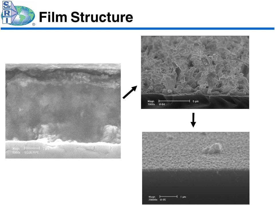
17 Conclusions Surface patterning of multi-layer thin films is a horizon technology that is demonstrating order of magnitude device improvements at laboratory scale. Deposition at speed and resolution requirements is the primary barrier for next generation plasmonic devices, metamaterials, and quantum technology Structure Zone Model Surface Patterning is a potential web coating process to achieve nanometer scale pattern resolution at high rates kent.coulter@swri.org Office: Cell:

18 BACK TO LIST

Laser Based Micro and Nanoscale Manufacturing and Materials Processing
 Laser Based Micro and Nanoscale Manufacturing and Materials Processing Faculty: Prof. Xianfan Xu Email: xxu@ecn.purdue.edu Phone: (765) 494-5639 http://widget.ecn.purdue.edu/~xxu Research Areas: Development
US News & World Report Graduate Program Comparison 1994 2015 Year ranking was published
 US News & World Report Graduate Program Comparison Year was published Select Findings from US News and World Report - Engineering Schools MIT Engineering Year that was released Rank 1 1 1 1 1 1 1 1 1 1
OPTIMIZING OF THERMAL EVAPORATION PROCESS COMPARED TO MAGNETRON SPUTTERING FOR FABRICATION OF TITANIA QUANTUM DOTS
 OPTIMIZING OF THERMAL EVAPORATION PROCESS COMPARED TO MAGNETRON SPUTTERING FOR FABRICATION OF TITANIA QUANTUM DOTS Vojtěch SVATOŠ 1, Jana DRBOHLAVOVÁ 1, Marian MÁRIK 1, Jan PEKÁREK 1, Jana CHOMOCKÁ 1,
TOURNAMENT RESULTS 1 N A T I O N A L I N T R A M U R A L - R E C R E A T I O N A L S P O R T S A S S O C I A T I O N
 TOURNAMENT RESULTS 1 N A T I O N A L I N T R A M U R A L - R E C R E A T I O N A L S P O R T S A S S O C I A T I O N 2005 USA Team Tennis National Campus Championship POOL A (A1) Texas A & M University
For Touch Panel and LCD Sputtering/PECVD/ Wet Processing
 production Systems For Touch Panel and LCD Sputtering/PECVD/ Wet Processing Pilot and Production Systems Process Solutions with over 20 Years of Know-how Process Technology at a Glance for Touch Panel,
Patrick F. Murphy, Ph.D., P.E., CFEI Senior Managing Engineer
 Senior Managing Engineer Professional Profile Dr. Murphy s background is in electrical and electronic engineering, including electronic and optoelectronic devices, circuits, and networks. His project experience
Improved Contact Formation for Large Area Solar Cells Using the Alternative Seed Layer (ASL) Process
 Process") Improved Contact Formation for Large Area Solar Cells Using the Alternative Seed Layer (ASL) Process Lynne Michaelson, Krystal Munoz, Jonathan C. Wang, Y.A. Xi*, Tom Tyson, Anthony Gallegos Technic Inc.,
Improved Contact Formation for Large Area Solar Cells Using the Alternative Seed Layer (ASL) Process Lynne Michaelson, Krystal Munoz, Jonathan C. Wang, Y.A. Xi*, Tom Tyson, Anthony Gallegos Technic Inc.,
Photolithography. Class: Figure 12.1. Various ways in which dust particles can interfere with photomask patterns.
 Photolithography Figure 12.1. Various ways in which dust particles can interfere with photomask patterns. 19/11/2003 Ettore Vittone- Fisica dei Semiconduttori - Lectio XIII 16 Figure 12.2. Particle-size
Lecture 12. Physical Vapor Deposition: Evaporation and Sputtering Reading: Chapter 12. ECE 6450 - Dr. Alan Doolittle
 Lecture 12 Physical Vapor Deposition: Evaporation and Sputtering Reading: Chapter 12 Evaporation and Sputtering (Metalization) Evaporation For all devices, there is a need to go from semiconductor to metal.
Demonstration of sub-4 nm nanoimprint lithography using a template fabricated by helium ion beam lithography
 Demonstration of sub-4 nm nanoimprint lithography using a template fabricated by helium ion beam lithography Wen-Di Li*, Wei Wu** and R. Stanley Williams Hewlett-Packard Labs *Current address: University
CREOL, College of Optics & Photonics, University of Central Florida
 OSE6650 - Optical Properties of Nanostructured Materials Optical Properties of Nanostructured Materials Fall 2013 Class 3 slide 1 Challenge: excite and detect the near field Thus far: Nanostructured materials
Excimer Laser Technology
 D. Basting G. Marowsky (Eds.) Excimer Laser Technology With 257 Figures ^y Springer Contents 1 Introduction 1 1.1 Introductory Remarks 1 1.1.1 The Unique Microstructuring Capabilities of Excimer Lasers
Novel inkjettable copper ink utilizing processing temperatures under 100 degrees C without the need of inert atmosphere
 Novel inkjettable copper ink utilizing processing temperatures under 100 degrees C without the need of inert atmosphere Printed Electronics Europe April 7-8, 2009 Dresden, Germany Dr. Zvi Yaniv Applied
IBS - Ion Beam Services
 IBS - Ion Beam Services Profile Technologies Devices & sensor fabricat ion Participation to R&D programs Researched partnership Présentation activité composant 1 Profile : Products and services Product
Psychology NRC Study S Rankings (1 of 6)
") 1 2 3 4 5 6 Princeton U. Harvard U. Stanford U. U. of Wisconsin at Madison Yale U. U. of Rochester U. of Michigan at Ann Arbor San Diego State U. and U. of California at San Diego Columbia U. U. of California
1 2 3 4 5 6 Princeton U. Harvard U. Stanford U. U. of Wisconsin at Madison Yale U. U. of Rochester U. of Michigan at Ann Arbor San Diego State U. and U. of California at San Diego Columbia U. U. of California
Psychology NRC Study R Rankings (1 of 6)
") 1 2 3 4 5 6 7 8 Princeton U. Harvard U. Stanford U. U. of Michigan at Ann Arbor Yale U. U. of Wisconsin at Madison U. of Rochester U. of California at Los Angeles Columbia U. Brown U. U. of Chicago U.
1 2 3 4 5 6 7 8 Princeton U. Harvard U. Stanford U. U. of Michigan at Ann Arbor Yale U. U. of Wisconsin at Madison U. of Rochester U. of California at Los Angeles Columbia U. Brown U. U. of Chicago U.
Arizona State University: A Strategic Perspective
 Arizona State University: A Strategic Perspective Michael M. Crow March 2005 Competition Competition Competition ASU is an enterprise embedded in a competitive arena An enterprise of: Competition information
Allopathic Medical Schools with Additional Science Course Requirements 2015
 Allopathic Medical Schools with Additional Science Course Requirements 2015 For many U.S. medical schools, the minimum required science courses for admission include one year each with laboratory of general
UC AND THE NATIONAL RESEARCH COUNCIL RATINGS OF GRADUATE PROGRAMS
 UC AND THE NATIONAL RESEARCH COUNCIL RATINGS OF GRADUATE PROGRAMS In the Fall of 1995, the University of California was the subject of some stunning news when the National Research Council (NRC) announced
School of Mathematics and Physics Performance Management Matrix Rolling 3-year targets 1. Experienced Lecturer/Senior Lecturer/Reader
 School of Mathematics and Physics Performance Management Matrix Rolling 3-year targets 1 Output measures per 3-year period Publications Lecturer (up to 3 years postprobation) 3 outputs per year (Physics
BENCHMARKING UNIVERSITY ADVANCEMENT PERFORMANCE
 F-14 BENCHMARKING UNIVERSITY ADVANCEMENT PERFORMANCE Benchmarking Data based on VSE stats (2007 survey results released on February 22, 2008) and peer lists including Universities in $2+ Billion-Dollar
Specifying Plasma Deposited Hard Coated Optical Thin Film Filters. Alluxa Engineering Staff
 Specifying Plasma Deposited Hard Coated Optical Thin Film Filters. Alluxa Engineering Staff December 2012 Specifying Advanced Plasma Deposited Hard Coated Optical Bandpass and Dichroic Filters. Introduction
Double Degree exchange programs taught at Phelma for KTH students
 Double Degree exchange programs taught at Phelma for KTH students Double Degree program for KTH students: In-coming Double Degree KTH students are registered in KTH and in Phelma, but they do not pay registration
Ultimate code quality on a wide variety of substrates. Coding and marking sample guide. CO2 Laser
 Ultimate code quality on a wide variety of substrates Coding and marking sample guide CO2 Laser Achieving the best laser mark is all about the specification process. Laser marking systems can generate
in the Rankings U.S. News & World Report
 in the Rankings UCLA performs very well in all the national and international rankings of the best public and private universities, including the most widely known list published by U.S. News & World Report.
Strategy for Functional Material Development in FUJIFILM
 証券コード 4901 Strategy for Functional Material Development in FUJIFILM - Global competency strategy for business innovation in Functional Material Industry - Sep. 24, 2013 FUJIFILM Corporation Development
US News & World Report Best Undergraduate Engineering Programs: Specialty Rankings 2014 Rankings Published in September 2013
 US News & World Report Best Undergraduate Engineering Programs: Specialty Rankings 2014 Rankings Published in September 2013 Aerospace/Aeronautical/Astronautical 2 Georgia Institute of Technology Atlanta,
U.S. News & World Report
 IN THE RANKINGS UCLA performs very well in all the national and international rankings of the best public and private universities, including the most widely known list published by U.S. News & World Report.
Technology White Papers nr. 13 Paul Holister Cristina Román Vas Tim Harper
 QUANTUM DOTS Technology White Papers nr. 13 Paul Holister Cristina Román Vas Tim Harper QUANTUM DOTS Technology White Papers nr. 13 Release Date: Published by Científica Científica, Ltd. www.cientifica.com
Production of Solar Energy Using Nanosemiconductors
 Production of Solar Energy Using Nanosemiconductors 1 Kiruthika S, 2 Dinesh Kumar M, 3 Surendar.A 1, 2 II year, KSR College of Engineering, Tiruchengode, Tamilnadu, India 3 Assistant Professor, KSR College
Q2 Which university will you be attending? American University (366) Arizona State University (367) Boston University (368) Brown University (439)
 Arizona State University (367) Boston University (368) Brown University (439)") Decline Offer Survey Thank you for considering the University of Washington during your search for a graduate degree program. We understand that many factors influence each applicant s decision in selecting
Decline Offer Survey Thank you for considering the University of Washington during your search for a graduate degree program. We understand that many factors influence each applicant s decision in selecting
Table 1. focus on Physics Graduate Degrees. Page 2. Number of Physics Departments with Graduate Programs, Academic Year 2007-08.
 www.aip.org/statistics One Physics Ellipse College Park, MD 274 31.29.37 stats@aip.org July 211 Physics Graduate Degrees Results from the Enrollments and Degrees & the Degree Recipient Follow-up Surveys
in the Rankings U.S. News & World Report
 UCLA performs very well in all the national and international rankings of the best public and private universities, including the most widely known list published by U.S. News & World Report. Following
How To Make A Plasma Control System
 XXII. Erfahrungsaustausch Mühlleiten 2015 Plasmaanalyse und Prozessoptimierung mittels spektroskopischem Plasmamonitoring in industriellen Anwendungen Swen Marke,, Lichtenau Thomas Schütte, Plasus GmbH,
III. Wet and Dry Etching
 III. Wet and Dry Etching Method Environment and Equipment Advantage Disadvantage Directionality Wet Chemical Solutions Atmosphere, Bath 1) Low cost, easy to implement 2) High etching rate 3) Good selectivity
Barrier Coatings: Conversion and Production Status
 Transparent SiO 2 Barrier Coatings: Conversion and Production Status E. Finson and J. Felts, Airco Coating Technology, Concord, CA Keywords: Permeation barrier coatings; Reactive evaporation; SiO 2 ABSTRACT
National Science Foundation
 Nanoscale Science and Engineering Education Programs at the National Science Foundation John S. (Spud) Bradley, Section Head Instructional Materials Development And Centers for Learning and Teaching, Division
Light management for photovoltaics. Ando Kuypers, TNO Program manager Solar
 Light management for photovoltaics Ando Kuypers, TNO Program manager Solar Global energy consumption: 500 ExaJoule/Year Solar irradiation on earth sphere: 5.000.000 ExaJoule/year 2 Capturing 0,01% covers
DISCUSSION ITEM ANNUAL REPORT ON NEWLY APPROVED INDIRECT COSTS AND DISCUSSION OF THE RECOVERY OF INDIRECT COSTS FROM RESEARCH BACKGROUND
 F2 Office of the President TO MEMBERS OF THE COMMITTEE ON FINANCE: For Meeting of November 17, 2010 DISCUSSION ITEM ANNUAL REPORT ON NEWLY APPROVED INDIRECT COSTS AND DISCUSSION OF THE RECOVERY OF INDIRECT
Houston Plating & Coatings
 Houston Plating & Coatings Electroless Nickel SBN QPQ TM Teflon Coating Polyurethane Multi-Coat Epoxy System Dry Film Lubricant Phosphate and Oil Xylan Fluoropolymer Molybdenum Disulfide Houston Plating
University Your selection: 169 universities
 University Your selection: 169 universities Level of study: bachelor, master Regions: United States, compareuni T eaching & Learning Research Knowledge T ransf er International Orientation Regional Engagement
Le nanotecnologie: dal Laboratorio al Mercato. Fabrizio Pirri Politecnico di Torino Istituto Italiano di Tecnologia
 Le nanotecnologie: dal Laboratorio al Mercato Fabrizio Pirri Politecnico di Torino Istituto Italiano di Tecnologia Materials & Processes for micro nanotechnologies Laboratory http://www.polito.it/micronanotech
National Bureau for Academic Accreditation And Education Quality Assurance LINGUISTICS # UNIVERSITY CITY STATE DEGREE MAJOR SPECIALTY RESTRICTION
 1 UNIVERSITY OF MASSACHUSETTS - BOSTON ~ BOSTON MA M 1 ARIZONA STATE UNIVERSITY - TEMPE TEMPE AZ MD ~ M for Linguistics is for Residential Program ONLY. The online option is not ~ M in Linguistics is for
Ultrahigh-efficiency solar cells based on nanophotonic design
 Ultrahigh-efficiency solar cells based on nanophotonic design Albert Polman Piero Spinelli Jorik van de Groep Claire van Lare Bonna Newman Erik Garnett Marc Verschuuren Ruud Schropp Wim Sinke Center for
Summary of Doctoral Degree Programs in Philosophy
 Summary of Doctoral Degree Programs in Philosophy, Opportunities, and Program Completion All data collected by the American Philosophical Association. The data in this publication have been provided by
The Italian High Tech Cluster for Nanotechnologies
 The Italian High Tech Cluster for Nanotechnologies Venezia, 16 gennaio 2007 Enzo Sisti Investor Relations, Veneto Nanotech Raffaele Franco Marketing Manager, Nanofab NANOTECHNOLOGIES: THAT S UNKNOWN! 1
Improving Printability of Functional Materials by. Laboratory of Paper Coating and Converting Martti Toivakka and Jouko Peltonen
 Improving Printability of Functional Materials by Controlled Substrate Topography and Chemistry Laboratory of Paper Coating and Converting Martti Toivakka and Jouko Peltonen Printed functionality & Paper
Graduate School Rankings By U.S. News & World Report: ENGINEERING SCHOOLS
 Rank Universities 1 University of California, Berkeley 2 Georgia Institute of Technology 3 University of Illinois, Urbana-Champaign 4 University of Texas, Austin 5 University of Michigan, Ann Arbor 6 Purdue
27.9% of the graduates responded. Respondents. Degree Surveys with Salaries Male Average Female Average. Table of Contents
 27.9% of the graduates responded Class # of Respondents % Males % Females Seniors 145 73.1% 26.9% Average Yearly Salary Salary Range Overall $125,457 $40,000 500,000 Male $132,434 $40,000 500,000 Female
Engineering Materials Research /DEVISER/
 DEVelopment of Infrastructure for Smart Engineering Materials Research /DEVISER/ A Czech structural funds project aimed for building a new public research infrastructure called Laboratory of Functional
A Data Based Assessment of Research Doctorate Programs in the United States
 A Data Based Assessment of Resear rch Doctorate Programs in the United States National Research Council Initial Analysis for University of California, Davis Graduat te Program in Civil and Environmental
METHODS FOR PULSED LASER DEPOSITION OF LARGE-AREA FILMS USING MORE THAN ONE TARGET
 Laser Physics 0 International Journal of Modern Physics: Conference Series Vol. 5 (0) 70 78 World Scientific Publishing Company DOI: 0.4/S009450078 METHODS FOR PULSED LASER DEPOSITION OF LARGE-AREA FILMS
Professor John Varcoe (Department of Chemistry, University of Surrey, UK) Plamen Atanassov
 Plamen Atanassov") Electronic Supplementary Material (ESI) for Energy & Environmental Science. This journal is The Royal Society of Chemistry 2014 Professor John Varcoe (Department of Chemistry, University of Surrey, UK)
Electronic Supplementary Material (ESI) for Energy & Environmental Science. This journal is The Royal Society of Chemistry 2014 Professor John Varcoe (Department of Chemistry, University of Surrey, UK)
WŝŽŶĞĞƌŝŶŐ > ĞdžƉĞƌŝĞŶĐĞ ƐŝŶĐĞ ϭϵϳϰ WŝĐŽƐƵŶ ^he > Ρ ZͲƐĞƌŝĞƐ > ƐLJƐƚĞŵƐ ƌŝěőŝŷő ƚśğ ŐĂƉ ďğƚǁğğŷ ƌğɛğăƌđś ĂŶĚ ƉƌŽĚƵĐƟŽŶ d, &hdhz K& d,/e &/>D /^, Z
 The ALD Powerhouse Picosun Defining the future of ALD Picosun s history and background date back to the very beginning of the field of atomic layer deposition. ALD was invented in Finland in 1974 by Dr.
Ion Beam Sputtering: Practical Applications to Electron Microscopy
 Ion Beam Sputtering: Practical Applications to Electron Microscopy Applications Laboratory Report Introduction Electron microscope specimens, both scanning (SEM) and transmission (TEM), often require a
UCLA in the Rankings. U.S. News & World Report
 UCLA performs very well in all the national and international rankings of the best public and private universities, including the most widely known list published by U.S. News & World Report. Following
Silicon-On-Glass MEMS. Design. Handbook
 Silicon-On-Glass MEMS Design Handbook A Process Module for a Multi-User Service Program A Michigan Nanofabrication Facility process at the University of Michigan March 2007 TABLE OF CONTENTS Chapter 1...
PLASMA TECHNOLOGY OVERVIEW
 PLASMA TECHNOLOGY OVERVIEW Plasmas are not a lab curiosity. Plasma processing has been an essential production tool for more than 30 years in the fabrication of microelectronic devices for example. Over
Filtration Technology
 Filtration Technology Capabilities Southwest Research Institute San Antonio, Texas Southwest Research Institute Founded in 1947 as an independent, nonprofit research and development organization, Southwest
Applications and Benefits of Multi-Walled Carbon Nanotubes (MWCNT)
") I Applications and Benefits of Multi-Walled Carbon Nanotubes (MWCNT) Table of Content 1 Introduction...1 2 Improved Properties...1 3 Potential Applications...1 3.1 Current / short-term applications...3
I Applications and Benefits of Multi-Walled Carbon Nanotubes (MWCNT) Table of Content 1 Introduction...1 2 Improved Properties...1 3 Potential Applications...1 3.1 Current / short-term applications...3
Miniaturizing Flexible Circuits for use in Medical Electronics. Nate Kreutter 3M
 Miniaturizing Flexible Circuits for use in Medical Electronics Nate Kreutter 3M Drivers for Medical Miniaturization Market Drivers for Increased use of Medical Electronics Aging Population Early Detection
College of Engineering Update - - I/UCRC CIMJSEA Mee9ng- -
 College of Engineering Update - - I/UCRC CIMJSEA Mee9ng- - Wayne T. Davis Dean College of Engineering December 1, 2014 1 College of Engineering Seven Academic Departments Chemical and Biomolecular Engineering
Materials for Organic Electronic. Jeremy Burroughes FRS FREng
 Materials for Organic Electronic Applications Jeremy Burroughes FRS FREng Introduction Organic Thin Film Transistors Organic Solar Cells and Photodiodes All Printed OLED Summary 4k2k 56 Displays Panasonic
Realization of Your Dream: Higher Study, Partnership, Collaboration Opportunities
 Realization of Your Dream: Higher Study, Partnership, Collaboration Opportunities Dr. Ashutosh Dutta, Ph.D. Lead Scientist, AT&T New Jersey, USA Email: ashutosh.dutta@ieee.org Realization of Your Dream
Update on the Status of Computational Science and Engineering in U.S. Graduate Programs
 HPCERC1999 023 28 September 1999 Update on the Status of Computational Science and Engineering in U.S. Graduate Programs Author Martha Lee Ennis The University of New Mexico High Performance Computing,
By Brian L. Yoder, Ph.D.
 Engineering by the Numbers By Brian L. Yoder, Ph.D. Bachelor s Degrees and Enrollment Degrees awarded to students graduating with a bachelor s degree from an engineering program increased by 7.5 percent
10 th Annual U.S. Department of Energy Small Business Conference
 10 th Annual U.S. Department of Energy Small Business Conference The Institution of Choice Annemarie Delgado, MA, MPA, CRA Assistant Director, Office of Sponsored Programs Norfolk State University 700
A CRITICAL NATIONAL NEED IDEA
 A CRITICAL NATIONAL NEED IDEA Advanced Manufacturing Technologies A Solution for Manufacturing High Volume Precision Micro Scale Components Submitted by: Rockford Engineering Associates LLC 605 Fulton
Soft lithography for diffractive microfabrications
 Soft lithography for diffractive microfabrications Liliana D Amico PhD Section: Materials Engineering XXVIII Cycle (3 Year) Mauro Casalboni, Fabio De Matteis, Paolo Prosposito, Roberta De Angelis Summary
TechVision 2020. A SYSTEMATIC INNOVATION SERENDIPITY ENGINE Convergence Begets Innovation Begets Growth
 TechVision 2020 A SYSTEMATIC INNOVATION SERENDIPITY ENGINE Convergence Begets Innovation Begets Growth Patent Activity Convergence Market Potential Funding Welcome to the Power Packed World of Top 50 Technologies
AC 2011-1023: INNOVATIVE GRADUATE PROGRAM IN NANOENGI- NEERING
 AC 2011-1023: INNOVATIVE GRADUATE PROGRAM IN NANOENGI- NEERING Ajit D. Kelkar, North Carolina A&T State University Dr. Ajit D. Kelkar is a Professor and Chairman of Nanoengineering department at Joint
National Nanotechnology Infrastructure Network Vol.4 # 5
 National Nanotechnology Infrastructure Network Vol.4 # 5 A Periodic Newsletter of NNIN News and Announcements October 2008 NNIN The National Nanotechnology Infrastructure Network consists of 12 nanotechnology
How To Understand Light And Color
 PRACTICE EXAM IV P202 SPRING 2004 1. In two separate double slit experiments, an interference pattern is observed on a screen. In the first experiment, violet light (λ = 754 nm) is used and a second-order
in the Rankings U.S. News & World Report
 in the Rankings UCLA performs very well in all the national and international rankings of the best public and private universities, including the most widely known list published by U.S. News & World Report.
Human Resources and Nanotechnology
 Human Resources and Nanotechnology Grant Black Indiana University South Bend November 14, 2007 Workshop on Statistics and Measurement Organization for Economic Cooperation and Development Paris, France
Chapter 1 Introduction to The Semiconductor Industry 2005 VLSI TECH. 1
 Chapter 1 Introduction to The Semiconductor Industry 1 The Semiconductor Industry INFRASTRUCTURE Industry Standards (SIA, SEMI, NIST, etc.) Production Tools Utilities Materials & Chemicals Metrology Tools
Fundamental Nanomaterials Research and Development: An Australian Perspective
 Fundamental Research and Development: An Australian Perspective Professor Max Lu FTSE, Fed Fellow, Director Http://www.arccfn.org.au Gross Domestic Expenditure on R&D Australia 10000 8000 Business Government
NAAB Accredited Program List
 Auburn University Alabama Architecture Bachelor's degree NAAB Tuskegee University Alabama Architecture Bachelor's degree NAAB Arizona State University Arizona Architecture Master's degree NAAB Frank Lloyd
Current U.S. News and World Report Rankings Public and Private *
 Undergraduate programs 2016 Engineering Engineering: 41 of 184 ahead of Dartmouth Michigan State of Business: 29 of 478 ahead of 2016 Business and specialty programs Brigham Young Management: 15 of 26
By Brian L. Yoder, Ph.D.
 Engineering by the Numbers By Brian L. Yoder, Ph.D. Bachelor s Degrees and Enrollment Engineering bachelor s degrees grew by 6 percent during the past year, reaching a total of 99,173 for 214. This continues
Tufts University Senior Survey 2010 Graduate Schools by Major Report
 Tufts University Graduate Schools by Major Report Note: This report includes both first and second major data, resulting in several students appearing twice under their first major and again under their
Allopathic Medical Schools with Additional Science Course Requirements as of July 2014
 Allopathic Medical Schools with Additional Science Course Requirements as of July 2014 For many U.S. medical schools, the minimum required science courses for admission include one year each with laboratory
Dot matrix Label ID Products. C Vinyl cloth labels. Dot Matrix. Features and benefits. Part numbering system
 Dot Matrix C Vinyl cloth labels Tyco Electronics C is a dot matrix printable vinyl coated cloth material with a permanent acrylic adhesive that is designed for application to irregular surfaces where conformability
Ferromagnetic resonance imaging of Co films using magnetic resonance force microscopy
 Ferromagnetic resonance imaging of Co films using magnetic resonance force microscopy B. J. Suh, P. C. Hammel, a) and Z. Zhang Condensed Matter and Thermal Physics, Los Alamos National Laboratory, Los
Solid State Electronics and Photonics Electrical and Computer Engineering The Ohio State University
 Solid State Electronics and Photonics Electrical and Computer Engineering The Ohio State University An Overview for Prospective Students http://www.ece.osu.edu/ssep SSEP Area: Who Are We? First Row Betty
Package Trends for Mobile Device
 Package Trends for Mobile Device On-package EMI Shield At CTEA Symposium Feb-10, 2015 Tatsuya Kawamura Marketing, Director TEL NEXX, Inc. Love Thinner Mobile? http://www.apple.com/ iphone is registered
Computational Nanoscience of Soft Matter
 ChE/MSE 557 Computational Nanoscience of Soft Matter Fall 2006 Instructor: Professor Sharon C. Glotzer Class meets: Tues 3:00-6:00 Location: Room 3336 BD, Duderstadt Center Room 3336 AC, Duderstadt Center
5. Scanning Near-Field Optical Microscopy 5.1. Resolution of conventional optical microscopy
 5. Scanning Near-Field Optical Microscopy 5.1. Resolution of conventional optical microscopy Resolution of optical microscope is limited by diffraction. Light going through an aperture makes diffraction
Pulsed laser deposition of organic materials
 Pulsed laser deposition of organic materials PhD theses Gabriella Kecskeméti Department of Optics and Quantum Electronics University of Szeged Supervisor: Dr. Béla Hopp senior research fellow Department
Summary of Doctoral Degree Programs in Philosophy
 Summary of Doctoral Degree Programs in Philosophy Faculty and Student Demographics All data collected by the ican Philosophical Association. The data in this publication have been provided by the departments
Association of American Medical College-Affiliated, Liaison Committee on Medical Education-
 Supplemental Digital Appendix 1 Association of American Medical College-Affiliated, Liaison Committee on Medical Education- Accredited U.S. Medical Schools Included in an Assessment of Clerkship Grading
Nanotechnology Education at SUNY Poly
 Nanotechnology Education at SUNY Poly Iulian Gherasoiu 1, Mohammed Abdallah 1, Digendra Das 1, Daniel K. Jones 1, Harry Efstathiadis 2 1 College of Engineering, SUNY Polytechnic Institute 2 Colleges of
2004 KICKOFF WEEKEND COLLEGES - ALPHABETICALLY
 Abilene Christian 1 Air Force 1 Akron 3 Ala.-Birmingham 4 Alabama 20 Alabama A&M 1 Alcorn State 4 Appalachian State 2 Arizona 14 Arizona State 23 Arkansas 13 Arkansas State 5 Arkansas-Monticello 1 Arkansas-Pine
College of Liberal Arts, 2002-2007 Cohorts: Placement of PhD Holders
 College of Liberal Arts, 00-007 Cohorts: Placement of PhD Holders Introduction This report features the PhD-placement portion of a study looking at all graduate students who enrolled in College of Liberal
A Ranking of Political Science Programs Based on Publications in Top Academic Journals and Book Presses
 A Ranking of Political Science Programs Based on Publications in Top Academic Journals and Book Presses THIS REPORT WAS CREATED AS AN INTERNAL DOCUMENT TO ACCOMPANY THE POLITICAL SCIENCE PRE-PROPOSAL FOR
SILA Sistema Integrato di Laboratori per l Ambiente. CENTRE FOR MICROSCOPY AND MICROANALYSIS Scientific coordinator: Prof.ssa Rosanna De Rosa
 CENTRE FOR MICROSCOPY AND MICROANALYSIS Scientific coordinator: Prof.ssa Rosanna De Rosa 0 The Centre for Microscopy and Microanalysis (CM2) is an interdisciplinary service centre, a comprehensive suite
703-697-5131/5132 (media) IMMEDIATE RELEASE April 21, 2011 703-571-3343 (public inquiry) DoD AWARDS $191 MILLION IN RESEARCH FUNDING
 IMMEDIATE RELEASE April 21, 2011 703-571-3343 (public inquiry) DoD AWARDS $191 MILLION IN RESEARCH FUNDING") ASSISTANT SECRETARY OF DEFENSE 3030 DEFENSE PENTAGON WASHINGTON, DC 20301-3030 RESEARCH AND ENGINEERING 703-697-5131/5132 (media) IMMEDIATE RELEASE April 21, 2011 703-571-3343 (public inquiry) DoD AWARDS
ASSISTANT SECRETARY OF DEFENSE 3030 DEFENSE PENTAGON WASHINGTON, DC 20301-3030 RESEARCH AND ENGINEERING 703-697-5131/5132 (media) IMMEDIATE RELEASE April 21, 2011 703-571-3343 (public inquiry) DoD AWARDS
Micro Motion 3098 Gas Specific Gravity Meter
 Product Data Sheet PS-001161, Rev. D April 2013 Micro Motion 3098 Gas Specific Gravity Meter Micro Motion density and concentration meters are built to tackle the most demanding process and fiscal applications.
GREEN NANOTECHNOLOGY. Geoffrey. Energy in the Built Environment. Solutions for Sustainability and. B. Smith Claes G. Granqvist.
 GREEN NANOTECHNOLOGY Solutions for Sustainability and Energy in the Built Environment Geoffrey B. Smith Claes G. Granqvist CRC Press Taylor & Francis Group Boca Raton London NewYork CRC Press is an imprint
Institution Amount Title Aiken Technical $195,484 Nuclear Welding Technical Education Project (NWTEP)
") 2014 Curriculum Development Grant Program Awards Institution Amount Title Aiken Technical College $195,484 Nuclear Welding Technical Education Project (NWTEP) Duke University $199,813 Development of New
2014 Curriculum Development Grant Program Awards Institution Amount Title Aiken Technical College $195,484 Nuclear Welding Technical Education Project (NWTEP) Duke University $199,813 Development of New