Chapter 1 DE2 115 Package Package Contents The DE2-115 Board Assembly...5. Chapter 2 Introduction of the Altera DE2 115 Board...
|
|
|
- Nathaniel Chase
- 8 years ago
- Views:
Transcription
1 1
2 CONTENTS Chapter 1 DE2 115 Package Package Contents The DE2-115 Board Assembly Getting Help...6 Chapter 2 Introduction of the Altera DE2 115 Board Layout and Components Block Diagram of the DE2-115 Board Power-up the DE2-115 Board...12 Chapter 3 DE2 115 Control Panel Control Panel Setup Controlling the LEDs, 7-segment Displays and LCD Display Switches and Push-buttons SDRAM/SRAM/EEPROM/Flash Controller and Program-mer USB Monitoring PS/2 Device SD Card RS-232 Communication VGA HSMC IR Receiver Overall Structure of the DE2-115 Control Panel...27 Chapter 4 Using the DE2 115 Board Configuring the Cyclone IV E FPGA Using Push-buttons and Switches

3 4.3 Using LEDs Using the 7-segment Displays Clock Circuitry Using the LCD Module High Speed Mezzanine Card Using the Expansion Header Using 14-pin General Purpose I/O Connector Using VGA Using the 24-bit Audio CODEC RS-232 Serial Port PS/2 Serial Port Gigabit Ethernet Transceiver TV Decoder Implementing a TV Encoder Using the USB Interface Using IR Using SRAM/SDRAM/FLASH/EEPROM/SD Card...63 Chapter 5 DE2 115 System Builder Introduction General Design Flow Using DE2-115 System Builder...71 Chapter 6 Examples of Advanced Demonstrations DE2-115 Factory Configuration TV Box Demonstration USB Paintbrush USB Device A Karaoke Machine SD Card Demonstration SD Card Music Player PS/2 Mouse Demonstration

4 6.9 IR Receiver Demonstration Music Synthesizer Demonstration Audio Recording and Playing Web Server Demonstration Chapter 7 Appendix Revision History Copyright Statement

5 Chapter 1 DE2-115 Package The DE2-115 package contains all components needed to use the DE2-115 board in conjunction with a computer that runs the Microsoft Windows OS. 1.1 Package Contents Figure 1-1 shows a photograph of the DE2-115 package. Figure 1-1 The DE2-115 package contents The DE2-115 package includes: The DE2-115 board. USB Cable for FPGA programming and control. DE2-115 System CD containing the DE2-115 documentation and supporting materials, including the User Manual, the Control Panel, System Builder and Altera Monitor Program utility, reference designs and demonstrations, device datasheets, tutorials, and a set of laboratory exercises. CD-ROMs containing Altera s Quartus II Web Edition and the Nios II Embedded Design Suit Evaluation Edition software. 4

6 Bag of six rubber (silicon) covers for the DE2-115 board stands. The bag also contains some extender pins, which can be used to facilitate easier probing with testing equipment of the board s I/O expansion headers. Clear plastic cover for the board. 12V DC desktop power supply. Remote controller 1.2 The DE2-115 Board Assembly To assemble the included stands for the DE2-115 board: Assemble a rubber (silicon) cover, as shown in Figure 1-2, for each of the six copper stands on the DE2-115 board The clear plastic cover provides extra protection, and is mounted over the top of the board by using additional stands and screws Figure 1-2 The feet for the DE2-115 board 5
 cover, as shown in Figure 1-2, for each of the six")
7 1.3 Getting Help Here are the addresses where you can get help if you encounter any problem: Altera Corporation 101 Innovation Drive San Jose, California, USA Terasic Technologies No. 356, Sec. 1, Fusing E. Rd. Jhubei City, HsinChu County, Taiwan, Tel.: Web: DE2-115.terasic.com 6

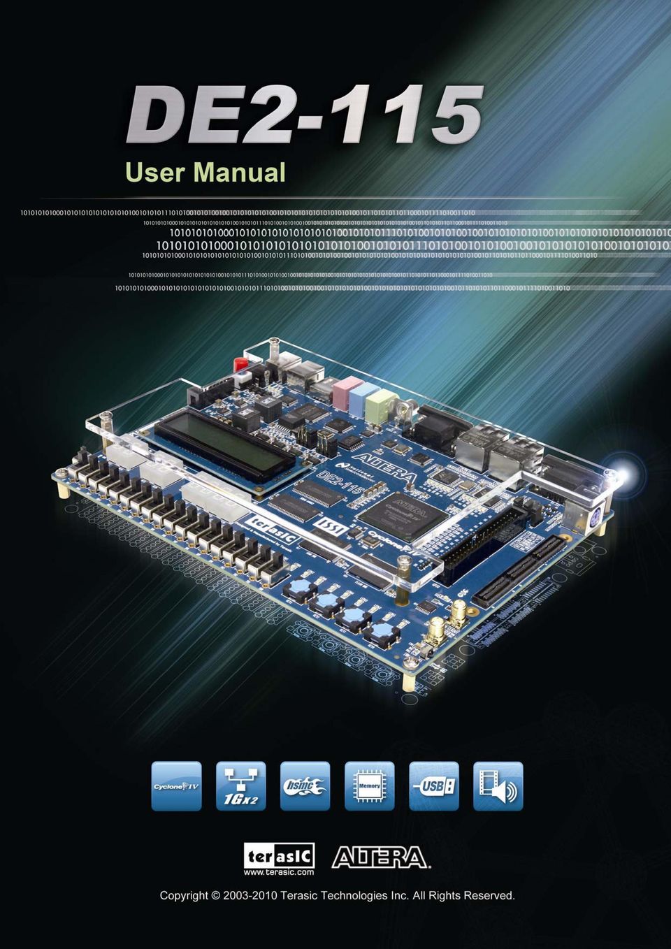
8 Chapter 2 Introduction of the Altera DE2-115 Board This chapter presents the features and design characteristics of the DE2-115 board. 2.1 Layout and Components A photograph of the DE2-115 board is shown in Figure 2-1 and Figure 2-2. It depicts the layout of the board and indicates the location of the connectors and key components. Figure 2-1 The DE2-115 board (top view) 7

9 Figure 2-2 The DE2-115 board (bottom view) The DE2-115 board has many features that allow users to implement a wide range of designed circuits, from simple circuits to various multimedia projects. The following hardware is provided on the DE2-115 board: Altera Cyclone IV 4CE115 FPGA device Altera Serial Configuration device EPCS64 USB Blaster (on board) for programming; both JTAG and Active Serial (AS) programming modes are supported 2MB SRAM Two 64MB SDRAM 8MB Flash memory SD Card socket 4 Push-buttons 18 Slide switches 18 Red user LEDs 9 Green user LEDs 50MHz oscillator for clock sources 24-bit CD-quality audio CODEC with line-in, line-out, and microphone-in jacks VGA DAC (8-bit high-speed triple DACs) with VGA-out connector TV Decoder (NTSC/PAL/SECAM) and TV-in connector 2 Gigabit Ethernet PHY with RJ45 connectors USB Host/Slave Controller with USB type A and type B connectors RS-232 transceiver and 9-pin connector PS/2 mouse/keyboard connector IR Receiver 2 SMA connectors for external clock input/output 8
 with VGA-out connector TV Decoder (NTSC/PAL/SECAM) and TV-in connector 2")
10 One 40-pin Expansion Header with diode protection One High Speed Mezzanine Card (HSMC) connector 16x2 LCD module In addition to these hardware features, the DE2-115 board has software support for standard I/O interfaces and a control panel facility for accessing various components. Also, the software is provided for supporting a number of demonstrations that illustrate the advanced capabilities of the DE2-115 board. In order to use the DE2-115 board, the user has to be familiar with the Quartus II software. The necessary knowledge can be acquired by reading the tutorials Getting Started with Altera s DE2-115 Board (tut_initialde2-115.pdf) and Quartus II Introduction (which exists in three versions based on the design entry method used, namely Verilog, VHDL or schematic entry). These tutorials are provided in the directory DE2_115_tutorials on the DE2-115 System CD that accompanies the DE2-115 kit and can also be found on Terasic s DE2-115 web pages. 2.2 Block Diagram of the DE2-115 Board Figure 2-3 gives the block diagram of the DE2-115 board. To provide maximum flexibility for the user, all connections are made through the Cyclone IV E FPGA device. Thus, the user can configure the FPGA to implement any system design. Figure 2-3 Block Diagram of DE

11 Following is more detailed information about the blocks in Figure 2-3: FPGA device Cyclone IV EP4CE115F29 device 114,480 LEs 432 M9K memory blocks 3,888 Kbits embedded memory 4 PLLs FPGA configuration JTAG and AS mode configuration EPCS64 serial configuration device On-board USB Blaster circuitry Memory devices 128MB (32Mx32bit) SDRAM 2MB (1Mx16) SRAM 8MB (4Mx16) Flash with 8-bit mode 32Kb EEPROM SD Card socket Provides SPI and 4-bit SD mode for SD Card access Connectors Two Ethernet 10/100/1000 Mbps ports High Speed Mezzanine Card (HSMC) Configurable I/O standards (voltage levels:3.3/2.5/1.8/1.5v) USB type A and B o Provide host and device controllers compliant with USB 2.0 o Support data transfer at full-speed and low-speed o PC driver available 10
 USB type A and B o Provide host and device controllers compliant with USB 2.")
12 40-pin expansion port o Configurable I/O standards (voltage levels:3.3/2.5/1.8/1.5v) VGA-out connector o VGA DAC (high speed triple DACs) DB9 serial connector for RS-232 port with flow control PS/2 mouse/keyboard Clock Three 50MHz oscillator clock inputs SMA connectors (external clock input/output) Audio 24-bit encoder/decoder (CODEC) Line-in, line-out, and microphone-in jacks Display 16x2 LCD module Switches and indicators 18 slide switches and 4 push-buttons switches 18 red and 9 green LEDs Eight 7-segment displays Other features Infrared remote-control receiver module TV decoder (NTSC/PAL/SECAM) and TV-in connector 11

13 Power Desktop DC input Switching and step-down regulators LM3150MH 2.3 Power-up the DE2-115 Board The DE2-115 board comes with a preloaded configuration bit stream to demonstrate some features of the board. This bit stream also allows users to see quickly if the board is working properly. To power-up the board perform the following steps: 1. Connect the provided USB cable from the host computer to the USB Blaster connector on the DE2-115 board. For communication between the host and the DE2-115 board, it is necessary to install the Altera USB Blaster driver software. If this driver is not already installed on the host computer, it can be installed as explained in the tutorial Getting Started with Altera's DE2-115 Board (tut_initialde2-115.pdf). This tutorial is available in the directory DE2_115_tutorials on the DE2-115 System CD. 2. Turn off the power by pressing the red ON/OFF switch before connecting the 12V adapter to the DE2-115 board. 3. Connect a VGA monitor to the VGA port on the DE2-115 board. 4. Connect your headset to the line-out audio port on the DE2-115 board. 5. Turn the RUN/PROG switch (SW19) on the left edge of the DE2-115 board to RUN position; the PROG position is used only for the AS Mode programming. 6. Recycle the power by turning the red power switch on the DE2-115 board OFF and ON again. At this point you should observe the following: All user LEDs are flashing All 7-segment displays are cycling through the numbers 0 to F The LCD display shows Welcome to the Altera DE2-115 The VGA monitor displays the image shown in Figure 2-4 Set the slide switch SW17 to the DOWN position; you should hear a 1-kHz sound. Be careful of the very loud volume for avoiding any discomfort Set the slide switch SW17 to the UP position and connect the output of an audio player to the line-in connector on the DE2-115 board; on your speaker or headset you should hear the music played from the audio player (MP3, PC, ipod, or the like) 12

14 You can also connect a microphone to the microphone-in connector on the DE2-115 board; your voice will be mixed with the music playing on the audio player Figure 2-4 The default VGA output pattern 13

15 Chapter 3 DE2-115 Control Panel The DE2-115 board comes with a Control Panel facility that allows users to access various components on the board from a host computer. The host computer communicates with the board through a USB connection. The facility can be used to verify the functionality of components on the board or be used as a debug tool while developing RTL code. This chapter first presents some basic functions of the Control Panel, then describes its structure in block diagram form, and finally describes its capabilities. 3.1 Control Panel Setup The Control Panel Software Utility is located in the directory DE2_115_tools/DE2_115_control_panel in the DE2-115 System CD. It's free of installation, just copy the whole folder to your host computer and launch the control panel by executing the DE2_115_ControlPanel.exe. (Windows 7 64-bit Users: If an error message that shows a missing jtag_client.dll file (cannot find jtag_client.dll) while the Control Panel is commencing, users should re-launch the DE4_ControlPanel.exe from the following directory (/DE2_115_tools/DE2_115_control_panel/win7_64bits)) Specific control circuit should be downloaded to your FPGA board before the control panel can request it to perform required tasks. The program will call Quartus II tools to download the control circuit to the FPGA board through USB-Blaster[USB-0] connection. To activate the Control Panel, perform the following steps: 1. Make sure Quartus II 10.0 or later version is installed successfully on your PC. 2. Set the RUN/PROG switch to the RUN position. 3. Connect the supplied USB cable to the USB Blaster port, connect the 12V power supply, and turn the power switch ON. 4. Start the executable DE2_115_ControlPanel.exe on the host computer. The Control Panel user interface shown in Figure 3-1 will appear. 14

16 5. The DE2_115_ControlPanel.sof bit stream is loaded automatically as soon as the DE2_115_control_panel.exe is launched. 6. In case the connection is disconnected, click on CONNECT where the.sof will be re-loaded onto the board. 7. Note, the Control Panel will occupy the USB port until you close that port; you cannot use Quartus II to download a configuration file into the FPGA until the USB port is closed. 8. The Control Panel is now ready for use; experience it by setting the ON/OFF status for some LEDs and observing the result on the DE2-115 board. Figure 3-1 The DE2-115 Control Panel The concept of the DE2-115 Control Panel is illustrated in Figure 3-2. The Control Circuit that performs the control functions is implemented in the FPGA board. It communicates with the Control Panel window, which is active on the host computer, via the USB Blaster link. The graphical interface is used to issue commands to the control circuit. It handles all requests and performs data transfers between the computer and the DE2-115 board. 15

17 Figure 3-2 The DE2-115 Control Panel concept The DE2-115 Control Panel can be used to light up LEDs, change the values displayed on 7-segment and LCD displays, monitor buttons/switches status, read/write the SDRAM, SRAM, EEPROM and Flash Memory, monitor the status of an USB device, communicate with the PS/2 mouse, output VGA color pattern to VGA monitor, verify functionality of HSMC connector I/Os, communicate with PC via RS-232 interface and read SD Card specification information. The feature of reading/writing a word or an entire file from/to the Flash Memory allows the user to develop multimedia applications (Flash Audio Player, Flash Picture Viewer) without worrying about how to build a Memory Programmer. 3.2 Controlling the LEDs, 7-segment Displays and LCD Display A simple function of the Control Panel is to allow setting the values displayed on LEDs, 7-segment displays, and the LCD character display. Choosing the LED tab leads to the window in Figure 3-3. Here, you can directly turn the LEDs on or off individually or by clicking Light All or Unlight All. 16
 without worrying about")
18 Figure 3-3 Controlling LEDs Choosing the 7-SEG tab leads to the window shown in Figure 3-4. From the window, directly use the left-right arrows to control the 7-SEG patterns on the DE2-115 board which are updated immediately. Note that the dots of the 7-SEGs are not enabled on DE2-115 board. Figure 3-4 Controlling 7-SEG display 17

19 Choosing the LCD tab leads to the window in Figure 3-5. Text can be written to the LCD display by typing it in the LCD box then pressing the Set button. Figure 3-5 Controlling the LCD display The ability to set arbitrary values into simple display devices is not needed in typical design activities. However, it gives the user a simple mechanism for verifying that these devices are functioning correctly in case a malfunction is suspected. Thus, it can be used for troubleshooting purposes. 3.3 Switches and Push-buttons Choosing the Switches tab leads to the window in Figure 3-6. The function is designed to monitor the status of slide switches and push-buttons in real time and show the status in a graphical user interface. It can be used to verify the functionality of the slide switches and push-buttons. 18

20 Figure 3-6 Monitoring switches and buttons The ability to check the status of push-button and slide switch is not needed in typical design activities. However, it provides users a simple mechanism for verifying if the buttons and switches are functioning correctly. Thus, it can be used for troubleshooting purposes. 3.4 SDRAM/SRAM/EEPROM/Flash Controller and Programmer The Control Panel can be used to write/read data to/from the SDRAM, SRAM, EEPROM, and Flash chips on the DE2-115 board. As an example, we will describe how the SDRAM may be accessed; the same approach is used to access the SRAM, EEPROM, and Flash. Click on the Memory tab and select SDRAM to reach the window in Figure

21 Figure 3-7 Accessing the SDRAM A 16-bit word can be written into the SDRAM by entering the address of the desired location, specifying the data to be written, and pressing the Write button. Contents of the location can be read by pressing the Read button. Figure 3-7 depicts the result of writing the hexadecimal value 06CA into offset address 200, followed by reading the same location. The Sequential Write function of the Control Panel is used to write the contents of a file into the SDRAM as follows: 1. Specify the starting address in the Address box. 2. Specify the number of bytes to be written in the Length box. If the entire file is to be loaded, then a checkmark may be placed in the File Length box instead of giving the number of bytes. 3. To initiate the writing process, click on the Write a File to Memory button. 4. When the Control Panel responds with the standard Windows dialog box asking for the source file, specify the desired file in the usual manner. The Control Panel also supports loading files with a.hex extension. Files with a.hex extension are ASCII text files that specify memory values using ASCII characters to represent hexadecimal values. For example, a file containing the line ABCDEF Defines eight 8-bit values: 01, 23, 45, 67, 89, AB, CD, EF. These values will be loaded consecutively into the memory. 20
22 The Sequential Read function is used to read the contents of the SDRAM and fill them into a file as follows: 1. Specify the starting address in the Address box. 2. Specify the number of bytes to be copied into the file in the Length box. If the entire contents of the SDRAM are to be copied (which involves all 128 Mbytes), then place a checkmark in the Entire Memory box. 3. Press Load Memory Content to a File button. 4. When the Control Panel responds with the standard Windows dialog box asking for the destination file, specify the desired file in the usual manner. Users can use the similar way to access the SRAM, EEPROM and Flash. Please note that users need to erase the Flash before writing data to it. 3.5 USB Monitoring The Control Panel provides users a USB monitoring tool which monitors the status of the USB devices connected to the USB port on the DE2-115 board. By plugging in a USB device to the USB host port of the board, the device type is displayed on the control window. Figure 3-8 shows a USB mouse plugged into the host USB port. Figure 3-8 USB Mouse Monitoring Tool 21
23 3.6 PS/2 Device The Control Panel provides users a PS/2 monitoring tool which monitors the real-time status of a PS/2 mouse connected to the DE2-115 board. The movement of the mouse and the status of the three buttons will be shown in the graphical and text interface. The mouse movement is translated as a position (x,y) with range from (0,0)~(1023,767). This function can be used to verify the functionality of the PS/2 connection. Follow the steps below to exercise the PS/2 Mouse Monitoring tool: 1. Choosing the PS/2 tab leads to the window in Figure Plug a PS/2 mouse to the PS/2 port on the DE2-115 board. 3. Press the Start button to start the PS/2 mouse monitoring process, and the button caption is changed from Start to Stop. In the monitoring process, the status of the PS/2 mouse is updated and shown in the Control Panel s GUI window in real-time. Press Stop to terminate the monitoring process. Figure 3-9 PS/2 Mouse Monitoring Tool 22
24 3.7 SD Card The function is designed to read the identification and specification information of the SD Card. The 4-bit SD MODE is used to access the SD Card. This function can be used to verify the functionality of the SD Card Interface. Follow the steps below to exercise the SD Card: 1. Choosing the SD Card tab leads to the window in Figure Insert an SD Card to the DE2-115 board, and then press the Read button to read the SD Card. The SD Card s identification, specification, and file format information will be displayed in the control window. Figure 3-10 Reading the SD Card Identification and Specification 3.8 RS-232 Communication The Control Panel allows users to verify the operation of the RS-232 serial communication interface on the DE The setup is established by connecting a RS pin male to female cable from the PC to the RS-232 port where the Control Panel communicates to the terminal emulator software on the PC, or vice versa. Alternatively, a RS-232 loopback cable can also be used if you do not wish to use the PC to verify the test. The Receive terminal window on the Control Panel monitors the serial communication status. Follow the steps below to initiate the RS-232 communication: 23
25 1. Choosing the RS-232 tab leads to the window in Figure Plug in a RS pin male to female cable from PC to RS-232 port or a RS-232 loopback cable directly to RS-232 port. 3. The RS-232 settings are provided below in case a connection from the PC is used: Baud Rate: Parity Check Bit: None Data Bits: 8 Stop Bits: 1 Flow Control (CTS/RTS): ON 4. To begin the communication, enter specific letters followed by clicking Send. During the communication process, observe the status of the Receive terminal window to verify its operation. Figure 3-11 RS-232 Serial Communication 3.9 VGA DE2-115 Control Panel provides VGA pattern function that allows users to output color pattern to LCD/CRT monitor using the DE2-115 board. Follow the steps below to generate the VGA pattern function: 24
26 1. Choosing the VGA tab leads to the window in Figure Plug a D-sub cable to VGA connector of the DE2-115 board and LCD/CRT monitor. 3. The LCD/CRT monitor will display the same color pattern on the control panel window. 4. Click the drop down menu shown in Figure 3-12 where you can output the selected color individually. Figure 3-12 Controlling VGA display 3.10 HSMC Select the HSMC tab to reach the window shown in Figure This function is designed to verify the functionality of the signals located on the HSMC connector. Before running the HSMC loopback verification test, follow the instruction noted under the Loopback Installation section and click on Verify. Please note to turn off the DE2-115 board before the HSMC loopback adapter is installed to prevent any damage to the board. The HSMC loopback adapter is not provided in the kit package but can be purchased through the website below: ( 25
27 Figure 3-13 HSMC loopback verification test performed under Control Panel 3.11 IR Receiver From the control panel, we can test the IR receiver on the DE2-115 by sending scan code from a remote controller. Figure 3-14 depicts the IR receiver window when the IR tab is pressed. When the scan code is received, the information will be displayed on the IR Receiver window represented in hexadecimal. Also, the pressed button on the remote controller will be indicated on the graphic of remote controller on the IR receiver window. Note that there exists several encoding form among different brands of remote controllers. Only the remote controller comes with the kit is confirmed to be compatible with this software. 26
28 Figure 3-14 Testing the IR receiver using remote controller 3.12 Overall Structure of the DE2-115 Control Panel The DE2-115 Control Panel is based on a Nios II SOPC system instantiated in the Cyclone IV E FPGA with software running on the on-chip memory. The software part is implemented in C code; the hardware part is implemented in Verilog HDL code with SOPC builder. The source code is not available on the DE2_115 System CD. To run the Control Panel, users should make the configuration according to Section 3.1. Figure 3-15 depicts the structure of the Control Panel. Each input/output device is controlled by the Nios II Processor instantiated in the FPGA chip. The communication with the PC is done via the USB Blaster link. The Nios II interprets the commands sent from the PC and performs the corresponding actions. 27
29 Figure 3-15 The block diagram of the DE2-115 control panel 28
30 Chapter 4 Using the DE2-115 Board This chapter gives instructions for using the DE2-115 board and describes each of its peripherals. 4.1 Configuring the Cyclone IV E FPGA The procedure for downloading a circuit from a host computer to the DE2-115 board is described in the tutorial Quartus II Introduction. This tutorial is found in the DE2_115_tutorials folder on the DE2-115 System CD. The user is encouraged to read the tutorial first, and treat the information below as a short reference. The DE2-115 board contains a serial configuration device that stores configuration data for the Cyclone IV E FPGA. This configuration data is automatically loaded from the configuration device into the FPGA every time while power is applied to the board. Using the Quartus II software, it is possible to reconfigure the FPGA at any time, and it is also possible to change the non-volatile data that is stored in the serial configuration device. Both types of programming methods are described below. 1. JTAG programming: In this method of programming, named after the IEEE standards Joint Test Action Group, the configuration bit stream is downloaded directly into the Cyclone IV E FPGA. The FPGA will retain this configuration as long as power is applied to the board; the configuration information will be lost when the power is turned off. 2. AS programming: In this method, called Active Serial programming, the configuration bit stream is downloaded into the Altera EPCS64 serial configuration device. It provides non-volatile storage of the bit stream, so that the information is retained even when the power supply to the DE2-115 board is turned off. When the board s power is turned on, the configuration data in the EPCS64 device is automatically loaded into the Cyclone IV E FPGA. JTAG Chain on DE2-115 Board To use JTAG interface for configuring FPGA device, the JTAG chain on DE2-115 must form a close loop that allows Quartus II programmer to detect FPGA device. Figure 4-1 illustrates the JTAG chain on DE2-115 board. Shorting pin1 and pin2 on JP3 can disable the JTAG signals on 29
31 HSMC connector that will form a close JTAG loop chain on DE2-115 board (See Figure 4-2). Thus, only the on board FPGA device (Cyclone IV E) will be detected by Quartus II programmer. If users want to include another FPGA device or interface containing FPGA device in the chain via HSMC connector, short pin2 and pin3 on JP3 to enable the JTAG signal ports on the HSMC connector. Figure 4-1 The JTAG chain on DE2-115 board Figure 4-2 The JTAG chain configuration header The sections below describe the steps used to perform both JTAG and AS programming. For both methods the DE2-115 board is connected to a host computer via a USB cable. Using this connection, the board will be identified by the host computer as an Altera USB Blaster device. The process for installing on the host computer the necessary software device driver that communicates with the USB Blaster is described in the tutorial Getting Started with Altera s DE2-115 Board (tut_initialde2-115.pdf). This tutorial is available on the DE2-115 System CD. 30
32 Configuring the FPGA in JTAG Mode Figure 4-3 illustrates the JTAG configuration setup. To download a configuration bit stream into the Cyclone IV E FPGA, perform the following steps: Ensure that power is applied to the DE2-115 board Configure the JTAG programming circuit by setting the RUN/PROG slide switch (SW19) to the RUN position (See Figure 4-4) Connect the supplied USB cable to the USB Blaster port on the DE2-115 board (See Figure 2-1) The FPGA can now be programmed by using the Quartus II Programmer to select a configuration bit stream file with the.sof filename extension Figure 4-3 The JTAG configuration scheme Figure 4-4 The RUN/PROG switch (SW19) is set in JTAG mode 31
33 Configuring the EPCS64 in AS Mode Figure 4-5 illustrates the AS configuration setup. To download a configuration bit stream into the EPCS64 serial configuration device, perform the following steps: Ensure that power is applied to the DE2-115 board. Connect the supplied USB cable to the USB Blaster port on the DE2-115 board (See Figure 4-5) Configure the JTAG programming circuit by setting the RUN/PROG slide switch (SW19) to the PROG position. The EPCS64 chip can now be programmed by using the Quartus II Programmer to select a configuration bit stream file with the.pof filename extension. Once the programming operation is finished, set the RUN/PROG slide switch back to the RUN position and then reset the board by turning the power switch off and back on; this action causes the new configuration data in the EPCS64 device to be loaded into the FPGA chip. Figure 4-5 The AS configuration scheme 4.2 Using Push-buttons and Switches The DE2-115 board provides four push-button switches as shown in Figure 4-6. Each of these switches is debounced using a Schmitt Trigger circuit, as indicated in Figure 4-7. The four outputs called KEY0, KEY1, KEY2, and KEY3 of the Schmitt Trigger devices are connected directly to the Cyclone IV E FPGA. Each push-button switch provides a high logic level when it is not pressed, and provides a low logic level when depressed. Since the push-button switches are debounced, they are appropriate for using as clock or reset inputs in a circuit. 32
34 Figure 4-6 Connections between the push-button and Cyclone IV E FPGA Pushbutton depressed Pushbutton released Before Debouncing Schmitt Trigger Debounced Figure 4-7 Switch debouncing There are also 18 slide switches on the DE2-115 board (See Figure 4-8). These switches are not debounced, and are assumed for use as level-sensitive data inputs to a circuit. Each switch is connected directly to a pin on the Cyclone IV E FPGA. When the switch is in the DOWN position (closest to the edge of the board), it provides a low logic level to the FPGA, and when the switch is in the UP position it provides a high logic level. 33
35 Figure 4-8 Connections between the slide switches and Cyclone IV E FPGA 4.3 Using LEDs There are 27 user-controllable LEDs on the DE2-115 board. Eighteen red LEDs are situated above the 18 Slide switches, and eight green LEDs are found above the push-button switches (the 9th green LED is in the middle of the 7-segment displays). Each LED is driven directly by a pin on the Cyclone IV E FPGA; driving its associated pin to a high logic level turns the LED on, and driving the pin low turns it off. Figure 4-9 shows the connections between LEDs and Cyclone IV E FPGA. Figure 4-9 Connections between the LEDs and Cyclone IV E FPGA A list of the pin names on the Cyclone IV E FPGA that are connected to the slide switches is given in Table 4-1. Similarly, the pins used to connect to the push-button switches and LEDs are displayed in Table 4-2 and Table 4-3, respectively. 34
36 Table 4-1 Pin Assignments for Slide Switches Signal Name FPGA Pin No. Description I/O Standard SW[0] PIN_AB28 Slide Switch[0] Depending SW[1] PIN_AC28 Slide Switch[1] Depending SW[2] PIN_AC27 Slide Switch[2] Depending SW[3] PIN_AD27 Slide Switch[3] Depending SW[4] PIN_AB27 Slide Switch[4] Depending SW[5] PIN_AC26 Slide Switch[5] Depending SW[6] PIN_AD26 Slide Switch[6] Depending SW[7] PIN_AB26 Slide Switch[7] Depending SW[8] PIN_AC25 Slide Switch[8] Depending SW[9] PIN_AB25 Slide Switch[9] Depending SW[10] PIN_AC24 Slide Switch[10] Depending SW[11] PIN_AB24 Slide Switch[11] Depending SW[12] PIN_AB23 Slide Switch[12] Depending SW[13] PIN_AA24 Slide Switch[13] Depending SW[14] PIN_AA23 Slide Switch[14] Depending SW[15] PIN_AA22 Slide Switch[15] Depending SW[16] PIN_Y24 Slide Switch[16] Depending SW[17] PIN_Y23 Slide Switch[17] Depending Table 4-2 Pin Assignments for Push-buttons Signal Name FPGA Pin No. Description I/O Standard KEY[0] PIN_M23 Push-button[0] Depending KEY[1] PIN_M21 Push-button[1] Depending KEY[2] PIN_N21 Push-button[2] Depending KEY[3] PIN_R24 Push-button[3] Depending Table 4-3 Pin Assignments for LEDs Signal Name FPGA Pin No. Description I/O Standard LEDR[0] PIN_G19 LED Red[0] 2.5V LEDR[1] PIN_F19 LED Red[1] 2.5V LEDR[2] PIN_E19 LED Red[2] 2.5V LEDR[3] PIN_F21 LED Red[3] 2.5V LEDR[4] PIN_F18 LED Red[4] 2.5V LEDR[5] PIN_E18 LED Red[5] 2.5V LEDR[6] PIN_J19 LED Red[6] 2.5V LEDR[7] PIN_H19 LED Red[7] 2.5V LEDR[8] PIN_J17 LED Red[8] 2.5V LEDR[9] PIN_G17 LED Red[9] 2.5V LEDR[10] PIN_J15 LED Red[10] 2.5V LEDR[11] PIN_H16 LED Red[11] 2.5V LEDR[12] PIN_J16 LED Red[12] 2.5V LEDR[13] PIN_H17 LED Red[13] 2.5V LEDR[14] PIN_F15 LED Red[14] 2.5V 35
37 LEDR[15] PIN_G15 LED Red[15] 2.5V LEDR[16] PIN_G16 LED Red[16] 2.5V LEDR[17] PIN_H15 LED Red[17] 2.5V LEDG[0] PIN_E21 LED Green[0] 2.5V LEDG[1] PIN_E22 LED Green[1] 2.5V LEDG[2] PIN_E25 LED Green[2] 2.5V LEDG[3] PIN_E24 LED Green[3] 2.5V LEDG[4] PIN_H21 LED Green[4] 2.5V LEDG[5] PIN_G20 LED Green[5] 2.5V LEDG[6] PIN_G22 LED Green[6] 2.5V LEDG[7] PIN_G21 LED Green[7] 2.5V LEDG[8] PIN_F17 LED Green[8] 2.5V 4.4 Using the 7-segment Displays The DE2-115 Board has eight 7-segment displays. These displays are arranged into two pairs and a group of four, behaving the intent of displaying numbers of various sizes. As indicated in the schematic in Figure 4-10, the seven segments (common anode) are connected to pins on Cyclone IV E FPGA. Applying a low logic level to a segment will light it up and applying a high logic level turns it off. Each segment in a display is identified by an index from 0 to 6, with the positions given in Figure Table 4-4 shows the assignments of FPGA pins to the 7-segment displays. Figure 4-10 Connections between the 7-segment display HEX0 and Cyclone IV E FPGA Table 4-4 Pin Assignments for 7-segment Displays Signal Name FPGA Pin No. Description I/O Standard HEX0[0] PIN_G18 Seven Segment Digit 0[0] 2.5V HEX0[1] PIN_F22 Seven Segment Digit 0[1] 2.5V HEX0[2] PIN_E17 Seven Segment Digit 0[2] 2.5V HEX0[3] PIN_L26 Seven Segment Digit 0[3] Depending HEX0[4] PIN_L25 Seven Segment Digit 0[4] Depending 36
38 HEX0[5] PIN_J22 Seven Segment Digit 0[5] Depending HEX0[6] PIN_H22 Seven Segment Digit 0[6] Depending HEX1[0] PIN_M24 Seven Segment Digit 1[0] Depending HEX1[1] PIN_Y22 Seven Segment Digit 1[1] Depending HEX1[2] PIN_W21 Seven Segment Digit 1[2] Depending HEX1[3] PIN_W22 Seven Segment Digit 1[3] Depending HEX1[4] PIN_W25 Seven Segment Digit 1[4] Depending HEX1[5] PIN_U23 Seven Segment Digit 1[5] Depending HEX1[6] PIN_U24 Seven Segment Digit 1[6] Depending HEX2[0] PIN_AA25 Seven Segment Digit 2[0] Depending HEX2[1] PIN_AA26 Seven Segment Digit 2[1] Depending HEX2[2] PIN_Y25 Seven Segment Digit 2[2] Depending HEX2[3] PIN_W26 Seven Segment Digit 2[3] Depending HEX2[4] PIN_Y26 Seven Segment Digit 2[4] Depending HEX2[5] PIN_W27 Seven Segment Digit 2[5] Depending HEX2[6] PIN_W28 Seven Segment Digit 2[6] Depending HEX3[0] PIN_V21 Seven Segment Digit 3[0] Depending HEX3[1] PIN_U21 Seven Segment Digit 3[1] Depending HEX3[2] PIN_AB20 Seven Segment Digit 3[2] Depending on JP6 HEX3[3] PIN_AA21 Seven Segment Digit 3[3] Depending on JP6 HEX3[4] PIN_AD24 Seven Segment Digit 3[4] Depending on JP6 HEX3[5] PIN_AF23 Seven Segment Digit 3[5] Depending on JP6 HEX3[6] PIN_Y19 Seven Segment Digit 3[6] Depending on JP6 HEX4[0] PIN_AB19 Seven Segment Digit 4[0] Depending on JP6 HEX4[1] PIN_AA19 Seven Segment Digit 4[1] Depending on JP6 HEX4[2] PIN_AG21 Seven Segment Digit 4[2] Depending on JP6 HEX4[3] PIN_AH21 Seven Segment Digit 4[3] Depending on JP6 HEX4[4] PIN_AE19 Seven Segment Digit 4[4] Depending on JP6 HEX4[5] PIN_AF19 Seven Segment Digit 4[5] Depending on JP6 HEX4[6] PIN_AE18 Seven Segment Digit 4[6] Depending on JP6 HEX5[0] PIN_AD18 Seven Segment Digit 5[0] Depending on JP6 HEX5[1] PIN_AC18 Seven Segment Digit 5[1] Depending on JP6 HEX5[2] PIN_AB18 Seven Segment Digit 5[2] Depending on JP6 HEX5[3] PIN_AH19 Seven Segment Digit 5[3] Depending on JP6 HEX5[4] PIN_AG19 Seven Segment Digit 5[4] Depending on JP6 HEX5[5] PIN_AF18 Seven Segment Digit 5[5] Depending on JP6 HEX5[6] PIN_AH18 Seven Segment Digit 5[6] Depending on JP6 HEX6[0] PIN_AA17 Seven Segment Digit 6[0] Depending on JP6 HEX6[1] PIN_AB16 Seven Segment Digit 6[1] Depending on JP6 HEX6[2] PIN_AA16 Seven Segment Digit 6[2] Depending on JP6 HEX6[3] PIN_AB17 Seven Segment Digit 6[3] Depending on JP6 HEX6[4] PIN_AB15 Seven Segment Digit 6[4] Depending on JP6 HEX6[5] PIN_AA15 Seven Segment Digit 6[5] Depending on JP6 HEX6[6] PIN_AC17 Seven Segment Digit 6[6] Depending on JP6 HEX7[0] PIN_AD17 Seven Segment Digit 7[0] Depending on JP6 HEX7[1] PIN_AE17 Seven Segment Digit 7[1] Depending on JP6 37
39 HEX7[2] PIN_AG17 Seven Segment Digit 7[2] Depending on JP6 HEX7[3] PIN_AH17 Seven Segment Digit 7[3] Depending on JP6 HEX7[4] PIN_AF17 Seven Segment Digit 7[4] Depending on JP6 HEX7[5] PIN_AG18 Seven Segment Digit 7[5] Depending on JP6 HEX7[6] PIN_AA14 Seven Segment Digit 7[6] 3.3V 4.5 Clock Circuitry The DE2-115 board includes one oscillator that produces 50 MHz clock signal. A clock buffer is used to distribute 50 MHz clock signal with low jitter to FPGA. The distributing clock signals are connected to the FPGA that are used for clocking the user logic. The board also includes two SMA connectors which can be used to connect an external clock source to the board or to drive a clock signal out through the SMA connector. In addition, all these clock inputs are connected to the phase locked loops (PLL) clock input pins of the FPGA to allow users to use these clocks as a source clock for the PLL circuit. The clock distribution on the DE2-115 board is shown in Figure The associated pin assignments for clock inputs to FPGA I/O pins are listed in Table 4-5. Figure 4-11 Block diagram of the clock distribution Table 4-5 Pin Assignments for Clock Inputs Signal Name FPGA Pin No. Description I/O Standard CLOCK_50 PIN_Y2 50 MHz clock input 3.3V CLOCK2_50 PIN_AG14 50 MHz clock input 3.3V CLOCK3_50 PIN_AG15 50 MHz clock input Depending on JP6 SMA_CLKOUT PIN_AE23 External (SMA) clock output Depending on JP6 SMA_CLKIN PIN_AH14 External (SMA) clock input 3.3V 38
40 4.6 Using the LCD Module The LCD module has built-in fonts and can be used to display text by sending appropriate commands to the display controller called HD Detailed information for using the display is available in its datasheet, which can be found on the manufacturer s website, and from the DE2_115_datasheets\LCD folder on the DE2-115 System CD. A schematic diagram of the LCD module showing connections to the Cyclone IV E FPGA is given in Figure The associated pin assignments appear in Table 4-6. Figure 4-12 Connections between the LCD module and Cyclone IV E FPGA *(1): Note the current LCD modules used on DE2-115 boards do not have backlight. Therefore the LCD_BLON signal should not be used in users design projects. Table 4-6 Pin Assignments for LCD Module Signal Name FPGA Pin No. Description I/O Standard LCD_DATA[7] PIN_M5 LCD Data[7] 3.3V LCD_DATA[6] PIN_M3 LCD Data[6] 3.3V LCD_DATA[5] PIN_K2 LCD Data[5] 3.3V LCD_DATA[4] PIN_K1 LCD Data[4] 3.3V LCD_DATA[3] PIN_K7 LCD Data[3] 3.3V 39
41 LCD_DATA[2] PIN_L2 LCD Data[2] 3.3V LCD_DATA[1] PIN_L1 LCD Data[1] 3.3V LCD_DATA[0] PIN_L3 LCD Data[0] 3.3V LCD_EN PIN_L4 LCD Enable 3.3V LCD_RW PIN_M1 LCD Read/Write Select, 0 = Write, 1 = Read 3.3V LCD_RS PIN_M2 LCD Command/Data Select, 0 = Command, 1 = Data 3.3V LCD_ON PIN_L5 LCD Power ON/OFF 3.3V LCD_BLON PIN_L6 LCD Back Light ON/OFF 3.3V 4.7 High Speed Mezzanine Card The DE2-115 development board contains a HSMC interface to provide a mechanism for extending the peripheral-set of a FPGA host board by means of add-on cards. This can address today s high speed signaling requirement as well as low-speed device interface support. The HSMC interface support JTAG, clock outputs and inputs, high speed LVDS and single-ended signaling. The HSMC connector connects directly to the Cyclone IV E FPGA with 82 pins. Signals HSMC_SDA and HSMC_SCLK share the same bus with the respected signals I2C_SDA and I2C_SCL of the WM8731 audio ship and ADV7180 TV decoder chip. Table 4-7 shows the maximum power consumption of the daughter card that connects to HSMC port. Table 4-7 Power Supply of the HSMC Supplied Voltage Max. Current Limit 12V 1A 3.3V 1.5A (1).Note the current levels indicated in Table 4-7 are based on 50% resource consumption. If the HSMC interface is utilized with design resources exceeding 50%, please notify our support (support@terasic.com). (2).If the HSMC loopback adapter is mounted, the I2C_SCL will be directly routed back to I2C_SDA. Because audio chip, TV decoder chip and HSMC share one I2C bus, therefore audio and video chip won t function correctly. The voltage level of the I/O pins on the HSMC connector can be adjusted to 3.3V, 2.5V, 1.8V, or 1.5V using JP7 (The default setting is 2.5V, see Figure 4-13). Because the HSMC I/Os are connected to Bank 5 & 6 of the FPGA and the VCCIO voltage (VCCIO5 & VCCIO6) of these banks are controlled by the header JP7, users can use a jumper to select the input voltage of VCCIO5 & VCCIO6 to 3.3V, 2.5V, 1.8V, and 1.5V to control the voltage level of the I/O pins. Table 4-8 lists the jumper settings of the JP7. 40
42 Figure 4-13 HSMC VCCIO supply voltage setting header Table 4-8 Jumper Settings for different I/O Standards JP7 Jumper Settings Supplied Voltage to VCCIO5 & VCCIO6 IO Voltage of HSMC Connector (JP8) Short Pins 1 and 2 1.5V 1.5V Short Pins 3 and 4 1.8V 1.8V Short Pins 5 and 6 2.5V 2.5V (Default) Short Pins 7 and 8 3.3V 3.3V Note: Users that connect a daughter card on the HSMC connector need to pay close attention on the I/O standard between DE2-115 HSMC connector pins and daughter card system. For example, if the I/O standard of HSMC pins on DE2-115 board is set to 1.8V, a daughter card with 3.3V I/O standard may not work properly on DE2-115 board due to I/O standard mismatch. Additionally, when LVDS is used as the I/O standard of the HSMC connector, the LVDS receivers need to assemble a 100 Ohm resistor between two input signals for each pairs as shown in Figure Table 4-9 shows all the pin assignments of the HSMC connector. 41
43 Figure 4-14 LVDS interface on HSMC connector and Cyclone IV E FPGA Signal Name HSMC_CLKIN0 HSMC_CLKIN_N1 HSMC_CLKIN_N2 HSMC_CLKIN_P1 HSMC_CLKIN_P2 HSMC_CLKOUT0 Table 4-9 Pin Assignments for HSMC connector FPGA Pin No. Description PIN_AH15 Dedicated clock input PIN_J28 PIN_Y28 PIN_J27 PIN_Y27 PIN_AD28 LVDS RX or CMOS I/O or differential clock input LVDS RX or CMOS I/O or differential clock input LVDS RX or CMOS I/O or differential clock input LVDS RX or CMOS I/O or differential clock input Dedicated clock output 42 I/O Standard Depending on JP6 Depending Depending Depending Depending Depending HSMC_CLKOUT_N1 PIN_G24 LVDS TX or CMOS I/O or differential clock input/output Depending HSMC_CLKOUT_N2 PIN_V24 LVDS TX or CMOS I/O or differential clock input/output Depending HSMC_CLKOUT_P1 PIN_G23 LVDS TX or CMOS I/O or differential clock input/output Depending HSMC_CLKOUT_P2 PIN_V23 LVDS TX or CMOS I/O or differential clock input/output Depending HSMC_D[0] PIN_AE26 LVDS TX or CMOS I/O Depending HSMC_D[1] PIN_AE28 LVDS RX or CMOS I/O Depending HSMC_D[2] PIN_AE27 LVDS TX or CMOS I/O Depending HSMC_D[3] PIN_AF27 LVDS RX or CMOS I/O Depending HSMC_RX_D_N[0] PIN_F25 LVDS RX bit 0n or CMOS I/O Depending
44 HSMC_RX_D_N[1] PIN_C27 Depending LVDS RX bit 1n or CMOS I/O HSMC_RX_D_N[2] PIN_E26 Depending LVDS RX bit 2n or CMOS I/O HSMC_RX_D_N[3] PIN_G26 Depending LVDS RX bit 3n or CMOS I/O HSMC_RX_D_N[4] PIN_H26 Depending LVDS RX bit 4n or CMOS I/O HSMC_RX_D_N[5] PIN_K26 Depending LVDS RX bit 5n or CMOS I/O HSMC_RX_D_N[6] PIN_L24 Depending LVDS RX bit 6n or CMOS I/O HSMC_RX_D_N[7] PIN_M26 Depending LVDS RX bit 7n or CMOS I/O HSMC_RX_D_N[8] PIN_R26 Depending LVDS RX bit 8n or CMOS I/O HSMC_RX_D_N[9] PIN_T26 Depending LVDS RX bit 9n or CMOS I/O HSMC_RX_D_N[10] PIN_U26 Depending LVDS RX bit 10n or CMOS I/O HSMC_RX_D_N[11] PIN_L22 Depending LVDS RX bit 11n or CMOS I/O HSMC_RX_D_N[12] PIN_N26 Depending LVDS RX bit 12n or CMOS I/O HSMC_RX_D_N[13] PIN_P26 Depending LVDS RX bit 13n or CMOS I/O HSMC_RX_D_N[14] PIN_R21 Depending LVDS RX bit 14n or CMOS I/O HSMC_RX_D_N[15] PIN_R23 Depending LVDS RX bit 15n or CMOS I/O HSMC_RX_D_N[16] PIN_T22 Depending LVDS RX bit 16n or CMOS I/O HSMC_RX_D_P[0] PIN_F24 Depending LVDS RX bit 0 or CMOS I/O HSMC_RX_D_P[1] PIN_D26 Depending LVDS RX bit 1 or CMOS I/O HSMC_RX_D_P[2] PIN_F26 Depending LVDS RX bit 2 or CMOS I/O HSMC_RX_D_P[3] PIN_G25 Depending LVDS RX bit 3 or CMOS I/O HSMC_RX_D_P[4] PIN_H25 Depending LVDS RX bit 4 or CMOS I/O HSMC_RX_D_P[5] PIN_K25 Depending LVDS RX bit 5 or CMOS I/O HSMC_RX_D_P[6] PIN_L23 Depending LVDS RX bit 6 or CMOS I/O 43
45 HSMC_RX_D_P[7] PIN_M25 Depending LVDS RX bit 7 or CMOS I/O HSMC_RX_D_P[8] PIN_R25 Depending LVDS RX bit 8 or CMOS I/O HSMC_RX_D_P[9] PIN_T25 Depending LVDS RX bit 9 or CMOS I/O HSMC_RX_D_P[10] PIN_U25 Depending LVDS RX bit 10 or CMOS I/O HSMC_RX_D_P[11] PIN_L21 Depending LVDS RX bit 11 or CMOS I/O HSMC_RX_D_P[12] PIN_N25 Depending LVDS RX bit 12 or CMOS I/O HSMC_RX_D_P[13] PIN_P25 Depending LVDS RX bit 13 or CMOS I/O HSMC_RX_D_P[14] PIN_P21 Depending LVDS RX bit 14 or CMOS I/O HSMC_RX_D_P[15] PIN_R22 Depending LVDS RX bit 15 or CMOS I/O HSMC_RX_D_P[16] PIN_T21 Depending LVDS RX bit 16 or CMOS I/O HSMC_TX_D_N[0] PIN_D28 Depending LVDS TX bit 0n or CMOS I/O HSMC_TX_D_N[1] PIN_E28 Depending LVDS TX bit 1n or CMOS I/O HSMC_TX_D_N[2] PIN_F28 Depending LVDS TX bit 2n or CMOS I/O HSMC_TX_D_N[3] PIN_G28 Depending LVDS TX bit 3n or CMOS I/O HSMC_TX_D_N[4] PIN_K28 Depending LVDS TX bit 4n or CMOS I/O HSMC_TX_D_N[5] PIN_M28 Depending LVDS TX bit 5n or CMOS I/O HSMC_TX_D_N[6] PIN_K22 Depending LVDS TX bit 6n or CMOS I/O HSMC_TX_D_N[7] PIN_H24 Depending LVDS TX bit 7n or CMOS I/O HSMC_TX_D_N[8] PIN_J24 Depending LVDS TX bit 8n or CMOS I/O HSMC_TX_D_N[9] PIN_P28 Depending LVDS TX bit 9n or CMOS I/O HSMC_TX_D_N[10] PIN_J26 Depending LVDS TX bit 10n or CMOS I/O HSMC_TX_D_N[11] PIN_L28 Depending LVDS TX bit 11n or CMOS I/O HSMC_TX_D_N[12] PIN_V26 Depending LVDS TX bit 12n or CMOS I/O HSMC_TX_D_N[13] PIN_R28 LVDS TX bit 13n or CMOS I/O Depending 44
46 HSMC_TX_D_N[14] PIN_U28 Depending LVDS TX bit 14n or CMOS I/O HSMC_TX_D_N[15] PIN_V28 Depending LVDS TX bit 15n or CMOS I/O HSMC_TX_D_N[16] PIN_V22 Depending LVDS TX bit 16n or CMOS I/O HSMC_TX_D_P[0] PIN_D27 Depending LVDS TX bit 0 or CMOS I/O HSMC_TX_D_P[1] PIN_E27 Depending LVDS TX bit 1 or CMOS I/O HSMC_TX_D_P[2] PIN_F27 Depending LVDS TX bit 2 or CMOS I/O HSMC_TX_D_P[3] PIN_G27 Depending LVDS TX bit 3 or CMOS I/O HSMC_TX_D_P[4] PIN_K27 Depending LVDS TX bit 4 or CMOS I/O HSMC_TX_D_P[5] PIN_M27 Depending LVDS TX bit 5 or CMOS I/O HSMC_TX_D_P[6] PIN_K21 Depending LVDS TX bit 6 or CMOS I/O HSMC_TX_D_P[7] PIN_H23 Depending LVDS TX bit 7 or CMOS I/O HSMC_TX_D_P[8] PIN_J23 Depending LVDS TX bit 8 or CMOS I/O HSMC_TX_D_P[9] PIN_P27 Depending LVDS TX bit 9 or CMOS I/O HSMC_TX_D_P[10] PIN_J25 Depending LVDS TX bit 10 or CMOS I/O HSMC_TX_D_P[11] PIN_L27 Depending LVDS TX bit 11 or CMOS I/O HSMC_TX_D_P[12] PIN_V25 Depending LVDS TX bit 12 or CMOS I/O HSMC_TX_D_P[13] PIN_R27 Depending LVDS TX bit 13 or CMOS I/O HSMC_TX_D_P[14] PIN_U27 Depending LVDS TX bit 14 or CMOS I/O HSMC_TX_D_P[15] PIN_V27 Depending LVDS TX bit 15 or CMOS I/O HSMC_TX_D_P[16] PIN_U22 Depending LVDS TX bit 16 or CMOS I/O 4.8 Using the Expansion Header The DE2-115 Board provides one 40-pin expansion header. The header connects directly to 36 pins of the Cyclone IV E FPGA, and also provides DC +5V (VCC5), DC +3.3V (VCC3P3), and two 45
47 GND pins. Figure 4-15 shows the I/O distribution of the GPIO connector. The maximum power consumption of the daughter card that connects to GPIO port is shown in Table Figure 4-15 GPIO Pin Arrangement Table 4-10 Power Supply of the Expansion Header Supplied Voltage Max. Current Limit 5V 1A 3.3V 1.5A Each pin on the expansion headers is connected to two diodes and a resistor that provides protection against high and low voltages. Figure 4-16 shows the protection circuitry for only one of the pin on the header, but this circuitry is included for all 36 data pins. Figure 4-16 Connections between the GPIO connector and Cyclone IV E FPGA 46
48 The voltage level of the I/O pins on the expansion headers can be adjusted to 3.3V, 2.5V, 1.8V, or 1.5V using JP6 (The default value is 3.3V, see Figure 4-17). Because the expansion I/Os are connected to Bank 4 of the FPGA and the VCCIO voltage (VCCIO4) of this bank is controlled by the header JP6, users can use a jumper to select the input voltage of VCCIO4 to 3.3V, 2.5V, 1.8V, and 1.5V to control the voltage level of the I/O pins. Table 4-11 lists the jumper settings of the JP6. The pin-outs of the JP6 appear in Figure Figure 4-17 GPIO VCCIO supply voltage setting header Table 4-11 Voltage Level Setting of the Expansion Headers Using JP6 JP6 Jumper Settings Supplied Voltage to VCCIO4 IO Voltage of Expansion Headers (JP5) Short Pins 1 and 2 1.5V 1.5V Short Pins 3 and 4 1.8V 1.8V Short Pins 5 and 6 2.5V 2.5V Short Pins 7 and 8 3.3V 3.3V (Default) 47
49 Note : Users who want to use daughter card on GPIO connector need to pay close attention to the I/O standard between DE2-115 GPIO connector pins and daughter card system. For example, if the I/O standard of GPIO pins on DE2-115 board is set to 1.8V, a daughter card with 3.3V I/O standard may not work properly on the DE2-115 board due to I/O standard mismatch. Figure 4-18 depicts the pin definition on the expansion connector for using these I/Os as LVDS transmitters. Due to the reason that the column I/Os of the FPGA the expansion pins connecting with can only support emulated LVDS transmitters, two single-ended output buffers and external resistors must be used as shown in Figure The associated I/O standard of these differential FPGA I/O pins on Quartus II project should set to LVDS_E_3R. Figure 4-18 Pin defined when using LVDS interface on GPIO FPGA pins The factory default setting on Rs resistor will be 47 ohm and Rp resistor will not be assembled for single-ended I/O standard application. For LVDS transmitter application, please assemble 120 and 170 ohm resistor on Rs and Rp position, respectively. Finally, Table 4-12 shows all the pin assignments of the GPIO connector. 48
Altera DE1 Board DE1. Development and Education Board. User Manual. Copyright 2006 Altera Corporation
 Altera DE1 Board DE1 Development and Education Board User Manual Version 1.1 Copyright 2006 Altera Corporation Altera DE1 Board CONTENTS Chapter 1 DE1 Package...1 1.1 Package Contents...1 1.2 The DE1 Board
Altera DE2 Board DE2. Development and Education Board. User Manual. Copyright 2006 Altera Corporation
 Altera DE2 Board DE2 Development and Education Board User Manual Version 1.4 Copyright 2006 Altera Corporation Altera DE2 Board CONTENTS Chapter 1 DE2 Package...1 1.1 Package Contents...1 1.2 The DE2 Board
2. Scope of the DE0 Board and Supporting Material
 1 Getting Started with Altera s DE0 Board This document describes the scope of Altera s DE0 Development and Education Board and the supporting materials provided by the Altera Corporation. It also explains
Chapter 1 Introduction... 3. 1. 1 Package Contents... 3. 1. 2 DE0-CV System CD... 4. 1. 3 Layout and Components... 4
 DE0-CV User Manual 1 www.terasic.com CONTENTS Chapter 1 Introduction... 3 1. 1 Package Contents... 3 1. 2 DE0-CV System CD... 4 1. 3 Layout and Components... 4 1. 4 Block Diagram of the Cyclone V Starter
Lab Experiment 1: The LPC 2148 Education Board
 Lab Experiment 1: The LPC 2148 Education Board 1 Introduction The aim of this course ECE 425L is to help you understand and utilize the functionalities of ARM7TDMI LPC2148 microcontroller. To do that,
HARDWARE MANUAL. BrightSign HD120, HD220, HD1020. BrightSign, LLC. 16795 Lark Ave., Suite 200 Los Gatos, CA 95032 408-852-9263 www.brightsign.
 HARDWARE MANUAL BrightSign HD120, HD220, HD1020 BrightSign, LLC. 16795 Lark Ave., Suite 200 Los Gatos, CA 95032 408-852-9263 www.brightsign.biz TABLE OF CONTENTS OVERVIEW... 1 Block Diagram... 2 Ports...
Digitale Signalverarbeitung mit FPGA (DSF) Soft Core Prozessor NIOS II Stand Mai 2007. Jens Onno Krah
 Soft Core Prozessor NIOS II Stand Mai 2007. Jens Onno Krah") (DSF) Soft Core Prozessor NIOS II Stand Mai 2007 Jens Onno Krah Cologne University of Applied Sciences www.fh-koeln.de jens_onno.krah@fh-koeln.de NIOS II 1 1 What is Nios II? Altera s Second Generation
(DSF) Soft Core Prozessor NIOS II Stand Mai 2007 Jens Onno Krah Cologne University of Applied Sciences www.fh-koeln.de jens_onno.krah@fh-koeln.de NIOS II 1 1 What is Nios II? Altera s Second Generation
Implementation of Web-Server Using Altera DE2-70 FPGA Development Kit
 1 Implementation of Web-Server Using Altera DE2-70 FPGA Development Kit A THESIS SUBMITTED IN PARTIAL FULFILLMENT OF THE REQUIREMENT OF FOR THE DEGREE IN Bachelor of Technology In Electronics and Communication
SKP16C62P Tutorial 1 Software Development Process using HEW. Renesas Technology America Inc.
 SKP16C62P Tutorial 1 Software Development Process using HEW Renesas Technology America Inc. 1 Overview The following tutorial is a brief introduction on how to develop and debug programs using HEW (Highperformance
USBSPYDER08 Discovery Kit for Freescale MC9RS08KA, MC9S08QD and MC9S08QG Microcontrollers User s Manual
 USBSPYDER08 Discovery Kit for Freescale MC9RS08KA, MC9S08QD and MC9S08QG Microcontrollers User s Manual Copyright 2007 SofTec Microsystems DC01197 We want your feedback! SofTec Microsystems is always on
Software User Guide UG-461
 Software User Guide UG-461 One Technology Way P.O. Box 9106 Norwood, MA 02062-9106, U.S.A. Tel: 781.329.4700 Fax: 781.461.3113 www.analog.com ezlinx icoupler Isolated Interface Development Environment
RC2200DK Demonstration Kit User Manual
 Demonstration Kit User Manual Table of contents TABLE OF CONTENTS... 1 QUICK INTRODUCTION... 2 INTRODUCTION... 3 DEMONSTRATION BOARD... 4 POWER SUPPLY SECTION... 5 RS-232 INTERFACE... 6 CONNECTORS... 7
USB to RS-422/485 Serial Adapter
 USB to RS-422/485 Serial Adapter User Manual Ver. 2.00 All brand names and trademarks are properties of their respective owners. Contents: Chapter 1: Introduction... 3 1.1 Product Introduction... 3 1.2
Getting Started with the Xilinx Zynq- 7000 All Programmable SoC Mini-ITX Development Kit
 Getting Started with the Xilinx Zynq- 7000 All Programmable SoC Mini-ITX Development Kit Table of Contents ABOUT THIS GUIDE... 3 ADDITIONAL DOCUMENTATION... 3 ADDITIONAL SUPPORT RESOURCES... 3 INTRODUCTION...
MasterBlaster Serial/USB Communications Cable User Guide
 MasterBlaster Serial/USB Communications Cable User Guide 101 Innovation Drive San Jose, CA 95134 www.altera.com Software Version: 80 Document Version: 1.1 Document Date: July 2008 Copyright 2008 Altera
Von der Hardware zur Software in FPGAs mit Embedded Prozessoren. Alexander Hahn Senior Field Application Engineer Lattice Semiconductor
 Von der Hardware zur Software in FPGAs mit Embedded Prozessoren Alexander Hahn Senior Field Application Engineer Lattice Semiconductor AGENDA Overview Mico32 Embedded Processor Development Tool Chain HW/SW
BE635 User Manual. Rev. V1.0. 2013-2014 Bolymin, Inc. All Rights Reserved.
 BE635 User Manual Rev. V1.0 2013-2014 Bolymin, Inc. All Rights Reserved. Copyright Copyright 2013-2014 BOLYMIN, INC. All rights reserved. No part of the materials may be reproduced, copied or translated
Chapter 6. Inside the System Unit. What You Will Learn... Computers Are Your Future. What You Will Learn... Describing Hardware Performance
 What You Will Learn... Computers Are Your Future Chapter 6 Understand how computers represent data Understand the measurements used to describe data transfer rates and data storage capacity List the components
Quick Installation. A Series of Intelligent Bar Code Reader with NeuroFuzzy Decoding. Quick Installation
 Quick Installation A Series of Intelligent Bar Code Reader with NeuroFuzzy Decoding This chapter intends to get your new FuzzyScan scanner working with your existing system within minutes. General instructions
Microcontroller Based Low Cost Portable PC Mouse and Keyboard Tester
 Leonardo Journal of Sciences ISSN 1583-0233 Issue 20, January-June 2012 p. 31-36 Microcontroller Based Low Cost Portable PC Mouse and Keyboard Tester Ganesh Sunil NHIVEKAR *, and Ravidra Ramchandra MUDHOLKAR
USB-Blaster Download Cable User Guide
 USB-Blaster Download Cable User Guide Subscribe UG-USB81204 101 Innovation Drive San Jose, CA 95134 www.altera.com TOC-2 Contents Introduction to USB-Blaster Download Cable...1-1 USB-Blaster Revision...1-1
LAN / WAN Connection Of Instruments with Serial Interface By Using a Terminal Server
 Products: EFA with EFA Scan, DVRM and DVMD with Realtime Monitor or Stream Explorer DVMD-B1 LAN / WAN Connection Of Instruments with Serial Interface By Using a Terminal Server Remote control of test and
USB - FPGA MODULE (PRELIMINARY)
") DLP-HS-FPGA LEAD-FREE USB - FPGA MODULE (PRELIMINARY) APPLICATIONS: - Rapid Prototyping - Educational Tool - Industrial / Process Control - Data Acquisition / Processing - Embedded Processor FEATURES:
DLP-HS-FPGA LEAD-FREE USB - FPGA MODULE (PRELIMINARY) APPLICATIONS: - Rapid Prototyping - Educational Tool - Industrial / Process Control - Data Acquisition / Processing - Embedded Processor FEATURES:
M68EVB908QL4 Development Board for Motorola MC68HC908QL4
 M68EVB908QL4 Development Board for Motorola MC68HC908QL4! Axiom Manufacturing 2813 Industrial Lane Garland, TX 75041 Email: Sales@axman.com Web: http://www.axman.com! CONTENTS CAUTIONARY NOTES...3 TERMINOLOGY...3
SBC8600B Single Board Computer
 SBC8600B Single Board Computer 720MHz TI s Sitara AM3359 ARM Cortex-A8 Microprocessor Onboard 512MByte DDR3 SDRAM and 512MByte NAND Flash UARTs, 2*USB Host and 1*OTG, 2*Ethernet, CAN, RS485, LCD/TSP, Audio,
T3 Mux M13 Multiplexer
 T3 Mux M13 Multiplexer User Manual [Type the abstract of the document here. The abstract is typically a short summary of the contents of the document. Type the abstract of the document here. The abstract
Multi-Profile CMOS Infrared Network Camera
 Multi-Profile CMOS Infrared Network Camera Quick Start Guide About multi-profile Multi-profile stands for simultaneously video stream. The Network Camera and Video Server can generate MPEG4 and MJPEG streaming
How To Use An Ams 5812 Pressure Sensor With A Usb Starter Kit
 User Guide USB Starter Kit AMS 5812 Phone:+49 (0)6131/91 0730-0 Fax: +49 (0)6131/91 073-30 Internet: E Mail: info@analogmicro.de Analog Microelectronics GmbH An der Fahrt 13, D 55124 Mainz May 2012 - Rev.
DKWF121 WF121-A 802.11 B/G/N MODULE EVALUATION BOARD
 DKWF121 WF121-A 802.11 B/G/N MODULE EVALUATION BOARD PRELIMINARY DATA SHEET Wednesday, 16 May 2012 Version 0.5 Copyright 2000-2012 Bluegiga Technologies All rights reserved. Bluegiga Technologies assumes
Table of Contents. Chapter1. Introduction...1. 1.1 Before Installation... 1 1.2 System Requirements... 1
 Table of Contents Chapter1. Introduction...1 1.1 Before Installation... 1 1.2 System Requirements... 1 Chapter2. IVS-110 1-Channel Internet Video Server...2 2.1 Package Content... 2 2.2 Physical Installation...
Introducing AVR Dragon
 Introducing AVR Dragon ' Front Side Back Side With the AVR Dragon, Atmel has set a new standard for low cost development tools. AVR Dragon supports all programming modes for the Atmel AVR device family.
2-Port RS232/422/485 Combo Serial to USB2.0 Adapter (w/ Metal Case and Screw Lock Mechanism) Installation Guide
 Installation Guide") 2-Port RS232/422/485 Combo Serial to USB2.0 Adapter (w/ Metal Case and Screw Lock Mechanism) Installation Guide 1. Introduction Thank you for purchasing this 2-Port RS232/422/485 Combo Serial to USB Adapter.
2-Port RS232/422/485 Combo Serial to USB2.0 Adapter (w/ Metal Case and Screw Lock Mechanism) Installation Guide 1. Introduction Thank you for purchasing this 2-Port RS232/422/485 Combo Serial to USB Adapter.
PolyBot Board. User's Guide V1.11 9/20/08
 PolyBot Board User's Guide V1.11 9/20/08 PolyBot Board v1.1 16 pin LCD connector 4-pin SPI port (can be used as digital I/O) 10 Analog inputs +5V GND GND JP_PWR 3-pin logic power jumper (short top 2 pins
Quick Start Guide. MRB-KW01 Development Platform Radio Utility Application Demo MODULAR REFERENCE BOARD
 Quick Start Guide MRB-KW01 Development Platform Radio Utility Application Demo MODULAR REFERENCE BOARD Quick Start Guide Get to Know the MRB-KW01x Module UART Selector ANT 1 RFIO (TX/RX) USB 2.0 Serial
Chapter 5 Cubix XP4 Blade Server
 Chapter 5 Cubix XP4 Blade Server Introduction Cubix designed the XP4 Blade Server to fit inside a BladeStation enclosure. The Blade Server features one or two Intel Pentium 4 Xeon processors, the Intel
11. High-Speed Differential Interfaces in Cyclone II Devices
 11. High-Speed Differential Interfaces in Cyclone II Devices CII51011-2.2 Introduction From high-speed backplane applications to high-end switch boxes, low-voltage differential signaling (LVDS) is the
EvB 5.1 v5 User s Guide
 EvB 5.1 v5 User s Guide Page 1 Contents Introduction... 4 The EvB 5.1 v5 kit... 5 Power supply...6 Programmer s connector...7 USB Port... 8 RS485 Port...9 LED's...10 Pushbuttons... 11 Potentiometers and
In-System Programmer USER MANUAL RN-ISP-UM RN-WIFLYCR-UM-.01. www.rovingnetworks.com 1
 RN-WIFLYCR-UM-.01 RN-ISP-UM In-System Programmer 2012 Roving Networks. All rights reserved. Version 1.1 1/19/2012 USER MANUAL www.rovingnetworks.com 1 OVERVIEW You use Roving Networks In-System-Programmer
SABRE Lite Development Kit
 SABRE Lite Development Kit Freescale i.mx 6Quad ARM Cortex A9 processor at 1GHz per core 1GByte of 64-bit wide DDR3 @ 532MHz UART, USB, Ethernet, CAN, SATA, SD, JTAG, I2C Three Display Ports (RGB, LVDS
1 Mi kołaj Z Mik ar ołaj Z zyc arzy ki cki
 1 Mikołaj Zarzycki NAND Flash SD Card Connector 256MB, 8bit I/F Push type, Up to 2GB/12.5Mbps USB Connector 1 x Device 2 x HOST, Dual-port LCD Module KEY Battery Holder 128 x 64 dots matrix structure 4
December 2002, ver. 1.0 Application Note 285. This document describes the Excalibur web server demonstration design and includes the following topics:
 Excalibur Web Server Demonstration December 2002, ver. 1.0 Application Note 285 Introduction This document describes the Excalibur web server demonstration design and includes the following topics: Design
Cart Interface Installation & Control Board Manual for M38 XP and RX Carts and Legacy M39 Carts
 Rubbermaid Medical Solutions Cart Interface Installation & Control Board Manual for M38 XP and RX Carts and Legacy M39 Carts REVISED FEBRUARY 25, 2010 Filename: Cart Interface Installation & Control Board
SF16-FMD. 16-Bit 3-D Sound Board with FM Radio. User Manual
 SF16-FMD 16-Bit 3-D Sound Board with FM Radio User Manual SF16-FMD 16-Bit 3-D Sound Board with FM Radio User Manual All rights reserved. No part of this publication may be produced, transmitted, transcribed,
isppac-powr1220at8 I 2 C Hardware Verification Utility User s Guide
 November 2005 Introduction Application Note AN6067 The isppac -POWR1220AT8 device from Lattice is a full-featured second-generation Power Manager chip. As part of its feature set, this device supports
Switch board datasheet EB007-00-1
 Switch board datasheet EB007-00-1 Contents 1. About this document... 2 2. General information... 3 3. Board layout... 4 4. Testing this product... 5 5. Circuit description... 6 Appendix 1 Circuit diagram
STIM202 Evaluation Kit
 Table of contents: 1 FEATURES... 2 2 GENERAL DESCRIPTIONS AND SYSTEM CONTENTS... 2 3 SYSTEM REQUIREMENTS... 2 4 GETTING STARTED... 3 4.1 INSTALLATION OF NI-SERIAL CABLE ASSEMBLY DRIVER... 3 4.2 INSTALLATION
Web Site: www.parallax.com Forums: forums.parallax.com Sales: sales@parallax.com Technical: support@parallax.com
 Web Site: www.parallax.com Forums: forums.parallax.com Sales: sales@parallax.com Technical: support@parallax.com Office: (916) 624-8333 Fax: (916) 624-8003 Sales: (888) 512-1024 Tech Support: (888) 997-8267
SDN INSTRUCTIONS 07/10, Ver 1.2. Somfy Digital Network (SDN) Installation and Programming
 Installation and Programming") Somfy Digital Network (SDN) Installation and Programming SSoomffyy SSyysst teemss IInncc.. 1 Table of Contents 1 General Information and Features... 3 1.1 ILT2 Motor... 3 1.2 SDN Switches... 4 1.3 ILT2
Somfy Digital Network (SDN) Installation and Programming SSoomffyy SSyysst teemss IInncc.. 1 Table of Contents 1 General Information and Features... 3 1.1 ILT2 Motor... 3 1.2 SDN Switches... 4 1.3 ILT2
LiveDesign Evaluation Board Technical Reference Manual. Technical reference manual for Altium s LiveDesign Evaluation Boards
 LiveDesign Evaluation Board Technical Reference Manual Technical reference manual for Altium s LiveDesign Evaluation Boards CAUTION THIS EQUIPMENT INCLUDES EXPOSED ELECTRONIC COMPONENTS THAT ARE HIGHLY
1-Port R422/485 Serial PCIe Card
 1-Port R422/485 Serial PCIe Card Installation Guide 1. Introduction Thank you for purchasing this 1-Port RS422/485 Serial PCI Express (PCIe) Card. It is a universal add in card that connects to a PC or
RS-232/422/485, Power over Ethernet
 IP-COM-M IP-COMi-M IP-COM-M PoE IP-COMi-M PoE RS-232 RS-232/422/485 RS-232, Power over Ethernet RS-232/422/485, Power over Ethernet Edition: September 2012 The computer programs provided with the hardware
1 Serial RS232 to Ethernet Adapter Installation Guide
 Installation Guide 10/100 Mbps LED (amber color ) Link/Activity LED (green color ) 1. Introduction Thank you for purchasing this 1-port RS232 to Ethernet Adapter (hereinafter referred to as Adapter ).
RAPID PROTOTYPING OF DIGITAL SYSTEMS Second Edition
 RAPID PROTOTYPING OF DIGITAL SYSTEMS Second Edition A Tutorial Approach James O. Hamblen Georgia Institute of Technology Michael D. Furman Georgia Institute of Technology KLUWER ACADEMIC PUBLISHERS Boston
SUDT AccessPort TM Advanced Terminal / Monitor / Debugger Version 1.37 User Manual
 SUDT AccessPort TM Advanced Terminal / Monitor / Debugger Version 1.37 User Manual Version 1.0 - January 20, 2015 CHANGE HISTORY Version Date Description of Changes 1.0 January 20, 2015 Initial Publication
RN-XV-RD2 Evaluation Board
 RN-XV-RD2 Evaluation Board 2012 Roving Networks. All rights reserved. -1.01Version 1.0 9/28/2012 USER MANUAL OVERVIEW This document describes the hardware and software setup for Roving Networks RN-XV-RD2
PM1122 INT DIGITAL INTERFACE REMOTE
 PM1122 INT DIGITAL INTERFACE REMOTE PM1122 INT front panel description: 1. Clear wireless remotes knob: push this button for more than 2 seconds to clear the list of all assigned wireless remote settings
Set up a Nios II project that specifies a desired hardware system and software program
 Altera Monitor Program Tutorial For Quartus II 11.0 1 Introduction This tutorial presents an introduction to the Altera Monitor Program, which can be used to compile, assemble, download and debug programs
WinCON8000-R2/R8. Hardware User s Manual
 WinCON8000-R2/R8 Compact Embedded Controller Hardware User s Manual REV 1.1 2004/10/22 1 Warranty All products manufactured by ICP DAS are warranted against defective materials for a period of one year
16-Port RS232 to USB2.0 High Speed Multi Serial Adapter (w/ Metal Case) Installation Guide
 Installation Guide") 16-Port RS232 to USB2.0 High Speed Multi Serial Adapter (w/ Metal Case) Installation Guide 1. Introduction Thank you for purchasing this 16-Port RS232 to USB2.0 High Speed Multi Serial Adapter. It is an
16-Port RS232 to USB2.0 High Speed Multi Serial Adapter (w/ Metal Case) Installation Guide 1. Introduction Thank you for purchasing this 16-Port RS232 to USB2.0 High Speed Multi Serial Adapter. It is an
PCAN-MicroMod Universal I/O Module with CAN Interface. User Manual. Document version 2.1.0 (2014-01-16)
") PCAN-MicroMod Universal I/O Module with CAN Interface User Manual Document version 2.1.0 (2014-01-16) Products taken into account Product Name Part number Model PCAN-MicroMod IPEH-002080 with firmware
PCAN-MicroMod Universal I/O Module with CAN Interface User Manual Document version 2.1.0 (2014-01-16) Products taken into account Product Name Part number Model PCAN-MicroMod IPEH-002080 with firmware
WIZ-Embedded WebServer User s Manual (Ver. 1.0)
") [텍스트 입력] WIZ-Embedded WebServer User s Manual (Ver. 1.0) 2007 WIZnet Inc. All Rights Reserved. For more information, visit our website at www.wiznet.co.kr Document History Information Revision Data Description
[텍스트 입력] WIZ-Embedded WebServer User s Manual (Ver. 1.0) 2007 WIZnet Inc. All Rights Reserved. For more information, visit our website at www.wiznet.co.kr Document History Information Revision Data Description
Installing MPU-401 Compatible Cards in Windows 95
 MPU-401 May 14, 1996 Compatible Cards Supplemental Notes Installing MPU-401 Compatible Cards in Windows 95 These notes are designed to help you install the following Roland MIDI cards and configure them
Troubleshooting Tips Lifestyle SA-2 & SA-3 Amplifier. Troubleshooting Tips
 Troubleshooting Tips Lifestyle SA-2 & SA-3 Amplifier Refer to the Lifestyle SA-2 & SA-3 Amplifier service manuals, part number 271720 for schematics, PCB layouts and parts lists. Preventative Repair Measures
Matrix 510/520 User Guide
 Matrix 510/520 User Guide Introduction: Matrix 510/520 are ARM9-based Linux ready industrial computer. The key features are as follow: Matrix 520 Layout 1. ARM920T ARM Thumb Processor with 200MIPS at 180MHz,
SVC400P/SVC800P. 4/8 Camera Live Tracking Vehicle DVR Installation Manual. Version 1.0
 SVC400P/SVC800P 4/8 Camera Live Tracking Vehicle DVR Installation Manual Version 1.0 1. MAIN FEATURES... 2 2. PRODUCT OVERVIEW... 2 3. DIMENSIONS... 4 4. PACKAGE CONTENTS... 5 5. MOUNTING AND ENVORNMENTAL
Advanced Data Capture and Control Systems
 Advanced Data Capture and Control Systems Tronisoft Limited Email: sales@tronisoft.com Web: www.tronisoft.com RS232 To 3.3V TTL User Guide RS232 to 3.3V TTL Signal Converter Modules P/N: 9651 Document
Bluetooth UART/RS232 Module
 Introduction BLUEMORE600 is a professional, slim, wireless module ready for integration in brand new or existing electronic products. Based on CSR chipset BC03MM it s fully compatible for Serial Port profiles.
Complete Train Control. Run Your Trains, Not Your Track! 1 PR3 Programmer 1 USB Cable 1 This Instruction sheet
 PR3 Complete Train Control Run Your Trains, Not Your Track! PR3 Decoder Programmer USB Programmer/Interface PR3 Features n Multifunction USB 2.0 PC connectivity for your railroad n Digitrax SoundLoader
SecureLinx Spider Duo Quick Start Guide
 SecureLinx Spider Duo Quick Start Guide SecureLinx Spider Duo Quick Start Guide SecureLinx Spider Duo QUICK START GUIDE CONTENTS Overview... 2 What s In The Box... 3 Installation and Network Settings...
EasyPIC4 User s Manual
 SOFTWARE AND HARDWARE SOLUTIONS FOR THE EMBEDDED WORLD MikroElektronika - Books - Compilers User s Manual PIC MICROCHIP DEVELOPMENT BOARD 3in1 mikro IN-CIRCUIT DEBUGGER USB 2.0 IN-CIRCUIT PROGRAMMER With
Getting Started. Chapter 1
 Chapter 1 Getting Started Thank you for choosing the 7728 v2.x Series Micro-ATX mainboard. The 7728 v2.x Series mainboards are based on Intel H61 chipsets for optimal system efficiency. Designed to fit
RN-WIFLY-EVAL-UM. WiFly Evaluation Kit. 2012 Roving Networks. All rights reserved. RN-WIFLY-EVAL-UM Version 1.32r 10/9/2012 USER MANUAL
 WiFly Evaluation Kit 2012 Roving Networks. All rights reserved. Version 1.32r 10/9/2012 USER MANUAL OVERVIEW This document describes the hardware and software setup for Roving Networks evaluation kits,
USER MANUAL GUIMGR Graphical User Interface Manager for FRM301/FRM401 Media Racks
 USER MANUAL GUIMGR Graphical User Interface Manager for FRM301/FRM401 Media Racks CTC Union Technologies Co., Ltd. Far Eastern Vienna Technology Center (Neihu Technology Park) 8F, No. 60 Zhouzi St. Neihu,
DK40 Datasheet & Hardware manual Version 2
 DK40 Datasheet & Hardware manual Version 2 IPC@CHIP DK40 Evaluation module Beck IPC GmbH http://www.bcl.de page 1 of 11 Table of contents Table of contents... 2 Basic description... 3 Characteristics...
MX PIC24F Educational Module User Manual
 MX PIC24F Educational Module User Manual Revision History Date Description Initial release. Table of Contents 1. Introduction... 3 1.1. Package Contents... 3 1.2. Key Hardware Features... 4 2. Hardware
Quick Start Guide for High Voltage Solar Inverter DC-AC Board EVM. Version 1.3
 Quick Start Guide for High Voltage Solar Inverter DC-AC Board EVM Version 1.3 Introduction This document talks about the quick start principles for the high voltage solar inverter DC-AC board. From this
Lab 1: Introduction to Xilinx ISE Tutorial
 Lab 1: Introduction to Xilinx ISE Tutorial This tutorial will introduce the reader to the Xilinx ISE software. Stepby-step instructions will be given to guide the reader through generating a project, creating
Elettronica dei Sistemi Digitali Costantino Giaconia SERIAL I/O COMMON PROTOCOLS
 SERIAL I/O COMMON PROTOCOLS RS-232 Fundamentals What is RS-232 RS-232 is a popular communications interface for connecting modems and data acquisition devices (i.e. GPS receivers, electronic balances,
STK500... User Guide
 STK500... User Guide Table of Contents Section 1 Introduction... 1-1 1.1 Starter Kit Features...1-1 1.2 Device Support...1-2 Section 2 Getting Started... 2-1 2.1 Unpacking the System...2-1 2.2 System
Keep it Simple Timing
 Keep it Simple Timing Support... 1 Introduction... 2 Turn On and Go... 3 Start Clock for Orienteering... 3 Pre Start Clock for Orienteering... 3 Real Time / Finish Clock... 3 Timer Clock... 4 Configuring
Quick Start Guide. Cisco Small Business. 200E Series Advanced Smart Switches
 Quick Start Guide Cisco Small Business 200E Series Advanced Smart Switches Welcome Thank you for choosing the Cisco 200E series Advanced Smart Switch, a Cisco Small Business network communications device.
Pre-tested System-on-Chip Design. Accelerates PLD Development
 Pre-tested System-on-Chip Design Accelerates PLD Development March 2010 Lattice Semiconductor 5555 Northeast Moore Ct. Hillsboro, Oregon 97124 USA Telephone: (503) 268-8000 www.latticesemi.com 1 Pre-tested
HARDWARE MANUAL HD222, HD1022. BrightSign, LLC. 16780 Lark Ave., Suite B Los Gatos, CA 95032 408-852-9263 www.brightsign.biz
 HARDWARE MANUAL HD222, HD1022 BrightSign, LLC. 16780 Lark Ave., Suite B Los Gatos, CA 95032 408-852-9263 www.brightsign.biz 1 TABLE OF CONTENTS Overview... 1 Block Diagram... 2 HD222... 3 HD1022... 4 Hardware
Ultra Thin Client TC-401 TC-402. Users s Guide
 Ultra Thin Client TC-401 TC-402 Users s Guide CONTENT 1. OVERVIEW... 3 1.1 HARDWARE SPECIFICATION... 3 1.2 SOFTWARE OVERVIEW... 4 1.3 HARDWARE OVERVIEW...5 1.4 NETWORK CONNECTION... 7 2. INSTALLING THE
CP2110-EK CP2110 EVALUATION KIT USER S GUIDE. 1. Kit Contents. 2. Relevant Documentation. 3. Software Setup
 CP2110 EVALUATION KIT USER S GUIDE 1. Kit Contents The CP2110 Evaluation Kit contains the following items: CP2110 Evaluation Board RS232 Serial Cable USB Cable DVD Quick Start Guide 2. Relevant Documentation
Creating a Project with PSoC Designer
 Creating a Project with PSoC Designer PSoC Designer is two tools in one. It combines a full featured integrated development environment (IDE) with a powerful visual programming interface. The two tools
Tutorial for MPLAB Starter Kit for PIC18F
 Tutorial for MPLAB Starter Kit for PIC18F 2006 Microchip Technology Incorporated. All Rights Reserved. WebSeminar Title Slide 1 Welcome to the tutorial for the MPLAB Starter Kit for PIC18F. My name is
AN4128 Application note
 Application note Demonstration board for Bluetooth module class 1 SBT2632C1A.AT2 Introduction This document describes the STEVAL-SPBT4ATV3 demonstration board (dongle) for the Bluetooth class 1 SPBT2632C1A.AT2
Welcome to the tutorial for the MPLAB Starter Kit for dspic DSCs
 Welcome to the tutorial for the MPLAB Starter Kit for dspic DSCs Welcome to this tutorial on Microchip s MPLAB Starter Kit for dspic Digital Signal Controllers, or DSCs. The starter kit is an all-in-one
USB 2.0 VGA ADAPTER USER MANUAL
 USB 2.0 VGA ADAPTER USER MANUAL CONTENTS INTRODUCTION... 3 FEATURES... 3 SYSTEM REQUIREMENTS... 3 PACKAGE CONTENTS... 3 SUPPORTED COMMON DISPLAY RESOLUTION... 4 TECHNICAL SPECIFICATIONS... 4 INSTALLATION
TCP/IP MODULE CA-ETHR-A INSTALLATION MANUAL
 TCP/IP MODULE CA-ETHR-A INSTALLATION MANUAL w w w. c d v g r o u p. c o m CA-ETHR-A: TCP/IP Module Installation Manual Page Table of Contents Introduction...5 Hardware Components... 6 Technical Specifications...
3-Port FireWire 800/400 PCI Host Card
 3-Port FireWire 800/400 PCI Host Card 400 FireWire Low Included FireWire Upgrade to FireWire800! U S E R S M A N U A L Low FireWire 400 Included Package Contents : 1 3-Port FireWire 800/400 PCI Host Card
MAX II Development Kit Getting Started User Guide
 MAX II Development Kit Getting Started User Guide 101 Innovation Drive San Jose, CA 95134 (408) 544-7000 www.altera.com P25-10351-01 Development Kit Version: 1.1.0 Document Version: 1.1.0 Document Date:
IOVU-571N ARM-based Panel PC
 IOVU-571N ARM-based Panel PC Features RISC-based Panel PC IOVU-57N Application Dimensions Ordering Information Specifications ARM-based Panel PC IOVU-571N Serial IOVU software support Packing List Options
RS232 Board datasheet
 RS232 Board datasheet Contents 1. About this document 2. General information 3. Board Layout 4. Getting Started 5. Circuit Description Appendix 1 Circuit Diagram Copyright 2004 Matrix Multimedia Limited
SA-9600 Surface Area Software Manual
 SA-9600 Surface Area Software Manual Version 4.0 Introduction The operation and data Presentation of the SA-9600 Surface Area analyzer is performed using a Microsoft Windows based software package. The
GV-Keyboard. User's Manual V2.0
 GV-Keyboard User's Manual V2.0 Before attempting to connect or operate this product, please read these instructions carefully and save this manual for future use. 2007 GeoVision, Inc. All rights reserved.
Orbit PCI Mk 2 Network Card. User Manual. Part No. 502566 Issue 4
 Orbit PCI Mk 2 Network Card User Manual Part No. 502566 Issue 4 Information in this document is subject to change without notice. Companies, names and data used in examples herein are fictitious unless
SP8 Programmers 硕 飞 科 技. User's Guide. TEL: 0755-8486 7757 FAX: 0755-8486 7941 WEB: www.sofi-tech.com
 硕 飞 科 技 SP8 Programmers User's Guide SHENZHEN SOFI TECHNOLOGY CO.,LTD. TEL: 0755-8486 7757 FAX: 0755-8486 7941 WEB: www.sofi-tech.com Publication Release Date: August 2011 Revision A1 Contents Chapter
Model 5511 Filler Controller User s Manual Version 1.1 October 2011
 Thompson Scale Company WEIGHING SYSTEMS & PACKAGING MACHINERY CONTROLS 2758 Bingle Road Houston, Texas 77055 Phone: 713/932-9071 Fax: 713/932-9379 www.thompsonscale.com Model 5511 Filler Controller User