Think Veranstaltung PG Tägerwilen & Gottlieben
|
|
|
- Deborah Williams
- 8 years ago
- Views:
Transcription
1 Think Veranstaltung PG Tägerwilen & Gottlieben 22. Januar, 2014 Tec-Sem Group AG Lohstampfstr. 11 CH-8274 Tägerwilen Phone

2 Tec-Sem in biz. Tec-Sem 33 Years Picture: Tec-Sem property / Page 2

3 History Gründung der Tec-Sem durch Jakob Blattner in Ermatingen, als Engineering Office Gründung der Tec-Sem AG in Ermatingen 1995 Umzug nach Tägerwilen HTC Formation of Tec-Sem Group AG as a holding company Creation of Tec-Sem sales & service subsidiaries in USA, Taiwan & Singapore Foundation of Tec-Sem Korea Inc. Foundation of Taiwan legal entity, Tec-Sem Taiwan Ltd / Page

4 Global Footprint Legal entities Tec-Sem Service hub Agent / Page

5 Transistor / Chip? Ein Transistor ist ein elektronisches Bauelement zum Schalten und Verstärken von elektrischen Signalen, ohne dabei mechanische Bewegungen auszuführen. Der Begriff Transistor ist eine Kurzform des englischen transfer resistor. Heute sind Millionen von Schaltungen auf einem Chip mit Strukturen kleiner 22nm. Vergleich Dicke Menschen Haar 50um -100um Erster Transistor 1925, Bild oben erster Intergierte Schaltung (IC) von Kilby 1958 Texas Instruments, 1 Schaltung. 1mm = 1000um = nm / Page

6 / Page Page 6

7 Wafer processing Logic chip für Smartphone über 800 process Schritte / Page

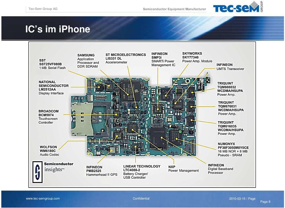
8 IC s im iphone / Page Page 8
9 Why I love our industry / Page 9

10 Why I love our industry / Page 10

11 No innovation w/o integrated circuits / Page 11

12 What drives our market 2 samples The internet of things will drive the next semiconductor growth wave Source: NXP Hans Rijns NXP / Page 12

13 Urbanization will drive M2M In 2007 about 50% of our world population lived in Urban environments By 2050 this is expected to be around 70-80% This drives the need for innovation in Smart Mobility and Smart Energy Source: NXP Hans Rijns NXP / Page 13

14 Sample1: Mobility Source: NXP Hans Rijns NXP / Page 14

15 Sample2: 2mart energy, home & building automation Source: NXP Hans Rijns NXP / Page 15

16 Semiconductor plays key role in energy supply chain Source: Infineon / Page 16

17 Der Gesamtmarkt / Page 17

18 Marktzyklen Growth [%] 80% 70% 60% 50% 40% 30% 20% 10% 0% -10% -20% -30% -40% -50% WW-GDP Electronics Semiconductor Semiconductor Equipment WW-GDP vs Electornics vs Semiconductors vs Semi-Equipment Marktwachstum ~15% p.a. 120% 70% 20 2% % Schlanke Organisation Kosten- & Cash Management Flexible Supply Chain Halbleiter- Eq.Markt Halbleitermarkt Elektronik BSP / Page 18

19 Revenue & profit targets 35'000'000 Revenue development 30'000'000 25'000'000 20'000'000 15'000'000 10'000'000 5'000' F / Page 19

20 Forecast 2014 REVENUE 2014 BY PRODUCT S 8% P 22% REVENUE 2014 BY TERRITORY Korea 6% CN 4% USA 36% TW 29% R 70% EUR 15% SG 10% / Page 20

21 CAPX by region vs TSAG revenue forecast Revenue 2014 by territory TW 29% Korea 6% CN 4% USA 36% Rest of the World Taiwan Korea Europe Japan North America Capital Expenditures by Region ($M) EUR 15% SG 10% / Page 21
22 IC Equipment revenues 70,000.0 IC MANUFACTURING EQUIPMENT MARKET HISTORY & FORECAST sales in $M per year and by main categories 60, , , , ,000.0 SERVICE & SUPPORT TOTAL IC ASSEMBLY EQUIPMENT TOTAL IC TEST and RELATED SYSTEMS TOTAL IC FABRICATION EQUIPMENT TOTAL IC AND RELATED EQUIPTMENT 10,000.0, Source: Data VLSI 06/12/ Chart Tec-Sem / Page 22
23 Segmentation Front-End revenues TOTAL IC FABRICATION EQUIPMENT MARKET HISTORY & FORECAST sales in $M per year Other Equipment Process Diagnostic Equipment Etching & Cleaning Tools Deposition & Related Tools Ion Implanters CMP Equipment Microlithography & Mask Making Equipment TOTAL IC AND RELATED EQUIPTMENT Source: Data VLSI 06/12/ Chart Tec-Sem / Page 23

24 References / Page
25 Market update (source IC Insights Feb.25th 2013) Top 5 spenders in 2013: Samsung Intel TSMC Globalfoundries SK Hynix Tec-Sem in Tec-Sem not YET in / Page 25
26 Just a few firms can afford to invest in advanced nodes / Page 26

27 Who has the capital to invest? / Page 27
28 FAB Automation Tec-Sem s Focal Point SEMICONDUCTOR MANUFACTURING IC s (Integrated Circuits) are produced in so called FAB s - fabrication automation environments. Silicon wafers form the basis in IC production and are manufactured in batch- or single-wafer processes. Wafer production involves several hundred process steps and various process equipment. Wafers are transported in wafer cassettes (FOUP s Front Opening Unified Pod). To reproduce structures on the wafers the design patterns are applied to the wafer by photolithography using photo masks or reticles. FAB AUTOMATION EQUIPMENT TEC-SEM FOCUS Reticles and wafers require adequate storage, management and transportation between the process steps. The automatic loading of single wafers or FOUP s into the process tools requires specific systems (EFEM Equipment Front End Module). Automated storage, identification, sorting, retrieving and transportation of wafers and reticles are the main tasks in fab automation. Wafer Reticle / Photomask FOUP / Page 28
29 Unique Technical Know-How INTERDISCIPLINARY EXPERTISE Extensive application know-how in handling, storage and identification of wafers and reticles. Clean-room design expertise (vacuum, purge technologies etc.). Thorough understanding of semiconductor fab automation requirements including IT integration and interfaces with process tools. State-of-the-art mechanical and software design. IP PORTFOLIO Tec-Sem holds over 50 patens or patent applications. TEC-CELL TECHNOLOGY High-precision, minimal-size, and clean storage cell for wafers or reticles. Defined environment with inert gas with special sealing to protect the increasingly sensitive substrates (line-width reduction). Enables high-speed wafer/reticle access and identification. Tec-Cell for Reticles Tec-Cell for Wafers / Page 29
30 Latest tool for T-Company Fab interface: HMI & maintenance access Foup stocker interface: 3 rotary laod-ports with E84 interface / Page
31 R&D Roadmap RX-Aquila Particle detection system Tec-Cell New Tec-Cell module & devices Flow Analysis new TCM / Page
32 Comparison - Concept CURRENT SYSTEM AQUILA Camera Scattered light Lightening Missing Area Reticle Detected Defect Light Scattering Method: Image depends on surface and structure No real image Bright field method with HiRes CCD camera: Image shows real defect outline / Page
33 Comparison Test Pellicle Holes CURRENT SYSTEM AQUILA Rough shape of big holes are visible Edges and real size of big holes Holes < 150um are still detectable / Page
34 Air-flow analysis Tec-Cell flow / Page 34
35 Reticle Management Solutions (Inspection) RXi-B (Basic) RXi-E (Extented) RXi-S (Storage) Tec-Cell Inside Basic reticle inspection system Built since 2010 Reticle qualification system Built since 2010 Reticle inspection & storage system Built since 2011 Stores up to 1600 reticles / Page
36 Reticle Management Solutions (Storage) RS RX RS Tec-Cell Inside Tec-Cell Inside Bare reticle stocker Build since 1994 Max reticles Not a bare stocker Built since 2008 Max reticles Not a bare stocker Built since 2010 Max reticles / Page
37 Q&A Thanks for your attention / Page 37
SUSS MICROTEC INVESTOR PRESENTATION. November 2015
 SUSS MICROTEC INVESTOR PRESENTATION November 2015 DISCLAIMER This presentation contains forward-looking statements relating to the business, financial performance and earnings of SUSS MicroTec AG and its
Chapter 1 Introduction to The Semiconductor Industry 2005 VLSI TECH. 1
 Chapter 1 Introduction to The Semiconductor Industry 1 The Semiconductor Industry INFRASTRUCTURE Industry Standards (SIA, SEMI, NIST, etc.) Production Tools Utilities Materials & Chemicals Metrology Tools
Introduction to Semiconductor Manufacturing Technology. Chapter 1, Introduction. Hong Xiao, Ph. D. hxiao89@hotmail.com
 Introduction to Semiconductor Manufacturing Technology Chapter 1, Introduction Hong Xiao, Ph. D. hxiao89@hotmail.com Hong Xiao, Ph. D. www2.austin.cc.tx.us/hongxiao/book.htm 1 Objective After taking this
Company Presentation. February 2011. Sustainable Technologies Conference. June 8, 2011
 Company Presentation Sustainable Technologies Conference February 2011 June 8, 2011 Disclaimer This presentation contains forward-looking statements relating to the business, financial performance and
DEVELOPMENTS & TRENDS IN FEOL MATERIALS FOR ADVANCED SEMICONDUCTOR DEVICES Michael Corbett mcorbett@linx-consulting.com Semicon Taiwan2015
 DEVELOPMENTS & TRENDS IN FEOL MATERIALS FOR ADVANCED SEMICONDUCTOR DEVICES Michael Corbett mcorbett@linx-consulting.com Semicon Taiwan2015 LINX BACKGROUND Linx Consulting 1. We help our clients to succeed
A Career that Revolutionises & Improves Lives
 OPTION GROUP B ELECTRONIC ENGINEERING presented by K Radha Krishnan Associate Professor, EEE 25 February 2015 1 A Career that Revolutionises & Improves Lives Scientists investigate that which already is,
SUSS MICROTEC INVESTOR PRESENTATION. May 2014
 SUSS MICROTEC INVESTOR PRESENTATION May 2014 DISCLAIMER This presentation contains forward-looking statements relating to the business, financial performance and earnings of SUSS MicroTec AG and its subsidiaries
SUSS MICROTEC INVESTOR PRESENTATION. November 2013
 SUSS MICROTEC INVESTOR PRESENTATION November 2013 DISCLAIMER This presentation contains forward-looking statements relating to the business, financial performance and earnings of SUSS MicroTec AG and its
SUSS MICROTEC INVESTOR PRESENTATION. September 2014
 SUSS MICROTEC INVESTOR PRESENTATION September 2014 DISCLAIMER This presentation contains forward-looking statements relating to the business, financial performance and earnings of SUSS MicroTec AG and
Robotics for Electronics Manufacturing
 Robotics for Electronics Manufacturing Presented to the IEEE Consultants Network of Silicon Valley (IEEE-CNSV) Tuesday, 8 June 2010 by Dr. Karl Mathia 1 Abstract Dr. Mathia will present topics from his
The Road to 450 mm Semiconductor Wafers Ira Feldman
 The Road to 450 mm Semiconductor Wafers Ira Feldman Feldman Engineering Corp. Why 450 mm Wafers? Technical Challenges Economic Challenges SoluBons Summary Overview 2 the number of transistors on a chip
Computing the Carbon Footprint Supply Chain for the Semiconductor Industry: A Learning Tool.
 Computing the Carbon Footprint Supply Chain for the Semiconductor Industry: A Learning Tool. Yasser Dessouky, Minnie H. Patel, and Tweesak Kaosamphan Industrial & Systems Engineering Charles W. Davidson
FOUP (Pod) contamination control solutions for 200 mm, 300 mm and 450 mm substrates. Jorgen Lundgren, Senior Applications Engineer Entegris GmbH
 contamination control solutions for 200 mm, 300 mm and 450 mm substrates. Jorgen Lundgren, Senior Applications Engineer Entegris GmbH") FOUP (Pod) contamination control solutions for 200 mm, 300 mm and 450 mm substrates Jorgen Lundgren, Senior Applications Engineer Entegris GmbH Agenda Entegris introduction FOUP (Pod) Contamination Control
FOUP (Pod) contamination control solutions for 200 mm, 300 mm and 450 mm substrates Jorgen Lundgren, Senior Applications Engineer Entegris GmbH Agenda Entegris introduction FOUP (Pod) Contamination Control
How To Make A Profit From Semiconductors
 Die Halbleiter Industrie in der Welt, in Europa und in Deutschland Dr. Andreas Wild Executive Director Content 1. Semiconductors, a few basic ideas 2. Semiconductors in the world 3. Semiconductors in Europe
Package Trends for Mobile Device
 Package Trends for Mobile Device On-package EMI Shield At CTEA Symposium Feb-10, 2015 Tatsuya Kawamura Marketing, Director TEL NEXX, Inc. Love Thinner Mobile? http://www.apple.com/ iphone is registered
Figure 1 Wafer with Notch
 Glass Wafer 2 SCHOTT is an international technology group with more than 125 years of experience in the areas of specialty glasses, materials and advanced technologies. With our high-quality products and
MACHINE VISION FOR SMARTPHONES. Essential machine vision camera requirements to fulfill the needs of our society
 MACHINE VISION FOR SMARTPHONES Essential machine vision camera requirements to fulfill the needs of our society INTRODUCTION With changes in our society, there is an increased demand in stateof-the art
UBS Technology Conference
 UBS Technology Conference London, 13 March 2013 Ulrich Pelzer Corporate Vice President Finance, Treasury & Investor Relations Table of Contents Infineon at a Glance Power Semiconductors and Manufacturing
Dual Integration - Verschmelzung von Wafer und Panel Level Technologien
 ERÖFFNUNG DES INNOVATIONSZENTRUMS ADAPTSYS Dual Integration - Verschmelzung von Wafer und Panel Level Technologien Dr. Michael Töpper BDT Introduction Introduction Why do we need such large machines to
Sustaining profitable growth Business focus and update
 Sustaining profitable growth Business focus and update Scott McGregor President and Chief Executive Officer Philips Semiconductors Financial Analysts Day 2004 What we mean by sustaining profitable growth
A Look Inside Smartphone and Tablets
 A Look Inside Smartphone and Tablets Devices and Trends John Scott-Thomas TechInsights Semicon West July 9, 2013 Teardown 400 phones and tablets a year Four areas: Customer Focus Camera Display Manufacturer
The Move to the next Silicon Wafer Size
 White Paper The Move to the next Silicon Wafer Size The Move to the next Silicon Wafer Size: A White Paper from the European Equipment and Materials 450mm Initiative (EEMI450) Introduction: Industry Dynamics
Lecture 30: Cleanroom design and contamination control
 Lecture 30: Cleanroom design and contamination control Contents 1 Introduction 1 2 Contaminant types 2 2.1 Particles.............................. 2 2.2 Metal ions............................. 4 2.3 Chemicals.............................
1.Introduction. Introduction. Most of slides come from Semiconductor Manufacturing Technology by Michael Quirk and Julian Serda.
 .Introduction If the automobile had followed the same development cycle as the computer, a Rolls- Royce would today cost $00, get one million miles to the gallon and explode once a year Most of slides
Rapid Prototyping and Development of Microfluidic and BioMEMS Devices
 Rapid Prototyping and Development of Microfluidic and BioMEMS Devices J. Sasserath and D. Fries Intelligent Micro Patterning System Solutions, LLC St. Petersburg, Florida (T) 727-522-0334 (F) 727-522-3896
Samsung Galaxy S6 Fingerprint Sensor New Synaptics Design
 Samsung Galaxy S6 Fingerprint Sensor New Synaptics Design Second generation Samsung Galaxy fingerprint sensor: same capacitive technology but totally different design For the second time Samsung introduces
Lithography Part I September, 5 th 2013
 7. Auswärtsseminar der Arbeitsgruppe Optische Technologien Leupold-Institut für Angewandte Naturwissenschaften (LIAN) der Westsächsischen Hochschule Zwickau Lithography Part I September, 5 th 2013 Heiko
Concevoir et produire des semiconducteurs en Europe: une Utopie? Let s have a look
 Concevoir et produire des semiconducteurs en Europe: une Utopie? Let s have a look Gérard MATHERON MIDIS MINATEC 24 avril 2009 1 Advanced Wafer Manufacturing Challenges Advanced Wafer Manufacturing Challenges
AIMS EUV. Status of Concept and Feasibility Study. Ulrich Stroessner* Heiko Feldmann** Wolfgang Harnisch* Dirk Hellweg** Sascha Perlitz*
 AIMS EUV Status of Concept and Feasibility Study 20.10.2010 Ulrich Stroessner* Heiko Feldmann** Wolfgang Harnisch* Dirk Hellweg** Sascha Perlitz* *Carl Zeiss SMS GmbH, Jena,Germany **Carl Zeiss SMT GmbH,
The Semiconductor Industry: Out in Front, but Lagging Behind Tom Mariano Published September, 2014
 As seen in The Semiconductor Industry: Out in Front, but Lagging Behind Tom Mariano Published September, 2014 Capital equipment suppliers must provide advanced analytical systems that leverage data generated
FOR HIGH-TECH PRODUCTION
 AUTOMATION & METROLOGY AUTOMATION & METROLOGY SOLUTIONS FOR HIGH-TECH PRODUCTION key technologies for multiple industries MANZ AG /// hightech solutions /// 5 2015 Acquisition of KLEO, a company of the
PCN Structure FY 13/14
 PCN Structure FY 13/14 A PCN FY 13/14 PCN text FY 13/14 QMS FY 12/14 Front End Materials A0101 Process Wafers CZ 150 mm CQT A0102 Process Wafers CZ 200 mm CQT A0103 Process Wafers FZ 150 mm CQT A0104 Process
Grad Student Presentation Topics PHGN/CHEN/MLGN 435/535: Interdisciplinary Silicon Processing Laboratory
 Grad Student Presentation Topics 1. Baranowski, Lauryn L. AFM nano-oxidation lithography 2. Braid, Jennifer L. Extreme UV lithography 3. Garlick, Jonathan P. 4. Lochner, Robert E. 5. Martinez, Aaron D.
Scanning Surface Inspection System with Defect-review SEM and Analysis System Solutions
 Scanning Surface Inspection System with -review SEM and Analysis System Solutions 78 Scanning Surface Inspection System with -review SEM and Analysis System Solutions Hideo Ota Masayuki Hachiya Yoji Ichiyasu
AN900 APPLICATION NOTE
 AN900 APPLICATION NOTE INTRODUCTION TO SEMICONDUCTOR TECHNOLOGY INTRODUCTION by Microcontroller Division Applications An integrated circuit is a small but sophisticated device implementing several electronic
IHK- Firmenbesuch Fachkräfte sichern in der Praxis Ralf Memmel Infineon Technologies AG. 27.06.2012 Page 1
 IHK- Firmenbesuch Fachkräfte sichern in der Praxis Ralf Memmel Infineon Technologies AG 27.06.2012 Page 1 IHK-Firmenbesuch Fachkräfte sichern in der Praxis Attraktive Arbeitswelten@Infineon Ralf Memmel
Creating Affordable Silicon
 Creating Affordable Silicon John Tinson VP Sales Sondrel 2016 03/05/2016 Presentation Title 1 The IoT Challenge Existing OEM s and start ups would benefit from a custom ASIC to prove their application
OLED - Technologie der Zukunft
 OLED - Technologie der Zukunft Dr. Manfred Weigand MERCK KGaA, Darmstadt, Germany Cleanzone 2014 Cathode Ray Tube (CRT) Source: Peter Littmann Source: Patrick Schindler Source: Bundesarchiv, Bild 183-H0812-0031-001
Thin Is In, But Not Too Thin!
 Thin Is In, But Not Too Thin! K.V. Ravi Crystal Solar, Inc. Abstract The trade-off between thick (~170 microns) silicon-based PV and thin (a few microns) film non-silicon and amorphous silicon PV is addressed
Substrate maturity and readiness in large volume to support mass adoption of ULP FDSOI platforms. SOI Consortium Conference Tokyo 2016
 Substrate maturity and readiness in large volume to support mass adoption of ULP FDSOI platforms Christophe Maleville Substrate readiness 3 lenses view SOI Consortium C1 - Restricted Conference Tokyo 2016
SEMI Microelectronic Manufacturing Supply Chain Quarterly Market Data - CYQ1 2016 www.semi.org/marketinfo
 SEMI Microelectronic Manufacturing Supply Chain Quarterly Market Data - CYQ1 2016 www.semi.org/marketinfo March 2016 Economic Trends Weakening Currency, especially Yen & Euro, dampened 2015 industry figures
OLED Status quo and Merck s position
 OLED Status quo and Merck s position Merck Information Day 2013 A Deep Dive into Merck s LC&OLED Business Dr. Udo Heider Vice President OLED Darmstadt, Germany June 26, 2013 Disclaimer Remarks All comparative
Contamination. Cleanroom. Cleanroom for micro and nano fabrication. Particle Contamination and Yield in Semiconductors.
 Fe Particles Metallic contaminants Organic contaminants Surface roughness Au Particles SiO 2 or other thin films Contamination Na Cu Photoresist Interconnect Metal N, P Damages: Oxide breakdown, metal
IBM Microelectronics East Fishkill, New York 1
 IBM Microelectronics East Fishkill, New York 1 John Kelly, senior vice president and group executive of the IBM technology Group claims that, High tech companies are turning to IBM for their high technology
How To Scale At 14 Nanomnemester
 14 nm Process Technology: Opening New Horizons Mark Bohr Intel Senior Fellow Logic Technology Development SPCS010 Agenda Introduction 2 nd Generation Tri-gate Transistor Logic Area Scaling Cost per Transistor
System Security Solutions for the connected world. www.infineon.com/ccs
 System Security Solutions for the connected world www.infineon.com/ccs Solutions for rising security demands The right balance between hardware-based and software-based security mechanisms allows you to
ni.com/vision NI Vision
 ni.com/vision NI Vision The NI Vision Approach Integrate NI LabVIEW graphical system design software across the entire NI vision hardware portfolio to create a flexible, open platform that reduces development
A Study of Haze Generation as Thin Film Materials
 A Study of Haze Generation as Thin Film Materials Ju-Hyun Kang, Han-Sun Cha*, Sin-Ju Yang, Chul-Kyu Yang, Jin-Ho Ahn*, Kee-Soo Nam, Jong-Min Kim**, Manish Patil**, Ik-Bum Hur** and Sang-Soo Choi** Blank
AMFitzgerald Company Overview
 AMFitzgerald Company Overview February 2015 12 th anniversary AMFitzgerald services MEMS Innovation MEMS Solutions Technology Strategy Creation of novel designs and IP Paths to manufacturing and market
(51) Int Cl.: G05F 3/26 (2006.01) G05F 3/24 (2006.01)
 Int Cl.: G05F 3/26 (2006.01) G05F 3/24 (2006.01)") (19) Europäisches Patentamt European Patent Office Office européen des brevets (11) EP 1 280 033 B1 (12) EUROPEAN PATENT SPECIFICATION (4) Date of publication and mention of the grant of the patent: 31.0.2006
(19) Europäisches Patentamt European Patent Office Office européen des brevets (11) EP 1 280 033 B1 (12) EUROPEAN PATENT SPECIFICATION (4) Date of publication and mention of the grant of the patent: 31.0.2006
Calibration of flow meters for liquids and gases
 Calibration of flow meters for liquids and gases Testo Industrial Services More certainty, better service. www.testotis.com Flow rate calibration Calibration of flow meters Due to the requirements of a
histaris Inline Sputtering Systems
 vistaris histaris Inline Sputtering Systems Inline Sputtering Systems with Vertical Substrate Transport Modular System for Different Applications VISTARIS Sputtering Systems The system with the brand name
VLSI Fabrication Process
 VLSI Fabrication Process Om prakash 5 th sem ASCT, Bhopal omprakashsony@gmail.com Manisha Kumari 5 th sem ASCT, Bhopal Manisha2686@gmail.com Abstract VLSI stands for "Very Large Scale Integration". This
Semiconductor design Outsourcing: Global trends and Indian perspective. Vasudevan A Date: Aug 29, 2003
 Semiconductor design Outsourcing: Global trends and Indian perspective Vasudevan A Date: Aug 29, 2003 Role of Semiconductors in Products Source: IC Insights Semiconductor content in end product increasing
SUSS MICROTEC INVESTOR PRESENTATION. May/June 2013
 SUSS MICROTEC INVESTOR PRESENTATION May/June 2013 DISCLAIMER This presentation contains forward-looking statements relating to the business, financial performance and earnings of SUSS MicroTec AG and its
Creating value in the semiconductor industry
 5 Creating value in the semiconductor industry In light of increasing consolidation throughout the semiconductor value chain, companies that wish to succeed must move quickly to close capability gaps.
www.pwc.com/chinasemicon China s impact on the semiconductor industry: 2015 update
 www.pwc.com/chinasemicon China s impact on the semiconductor industry: 2015 update Technology Institute Groups 1-4 January 2016 1 Group 1: China s semiconductor market For the fourth consecutive year China
History 02.02.2010. www.roodmicrotec.com
 Zwolle Dresden Nördlingen Stuttgart certified by. History - 1969: Foundation of German Signetics GmbH, test and assembly location, in Nördlingen (Germany) - 1974: Takeover by Philips Semiconductors - 1983:
SUSS MICROTEC INVESTOR PRESENTATION. April 2013
 SUSS MICROTEC INVESTOR PRESENTATION April 2013 DISCLAIMER This presentation contains forward-looking statements relating to the business, financial performance and earnings of SUSS MicroTec AG and its
Photovoltaic Power: Science and Technology Fundamentals
 Photovoltaic Power: Science and Technology Fundamentals Bob Clark-Phelps, Ph.D. Evergreen Solar, Inc. Renewable Energy Seminar, Nov. 2, 2006 Photovoltaic Principle Energy Conduction Band electron Energy
Low Power and Reliable SRAM Memory Cell and Array Design
 Springer Series in Advanced Microelectronics 31 Low Power and Reliable SRAM Memory Cell and Array Design Bearbeitet von Koichiro Ishibashi, Kenichi Osada 1. Auflage 2011. Buch. XI, 143 S. Hardcover ISBN
Nasdaq: ASYS. Amtech Systems, Inc. Solar & Semiconductor Solutions. J.S. Whang Chairman & Chief Executive Officer
 Amtech Systems, Inc. Nasdaq: ASYS 25th LISTING ANNIVERSARY ASYS / NASDAQ J.S. Whang Chairman & Chief Executive Officer Brad Anderson Chief Financial Officer January 13-14, 2010 1 Safe Harbor Statement
How To Make Money From Semiconductor Production
 ASML 2011 Third Quarter Results Confirming expectation for record sales year Oct 12, 2011 / Slide 1 Safe Harbor "Safe Harbor" Statement under the US Private Securities Litigation Reform Act of 1995: the
Figure 1. New Wafer Size Ramp Up as a Percentage of World Wide Silicon Area Versus Years Elapsed Since the New Size Was Introduced [1].
![Figure 1. New Wafer Size Ramp Up as a Percentage of World Wide Silicon Area Versus Years Elapsed Since the New Size Was Introduced [1].](/thumbs/23/1973496.jpg "Figure 1. New Wafer Size Ramp Up as a Percentage of World Wide Silicon Area Versus Years Elapsed Since the New Size Was Introduced [1].") White Paper Forecasting the 45mm Ramp Up IC Knowledge LLC, PO Box 2, Georgetown, MA 1833 Tx: (978) 352 761, Fx: (978) 352 387, email: info@icknowledge.com Introduction The introduction and ramp up of 45mm
White Paper Forecasting the 45mm Ramp Up IC Knowledge LLC, PO Box 2, Georgetown, MA 1833 Tx: (978) 352 761, Fx: (978) 352 387, email: info@icknowledge.com Introduction The introduction and ramp up of 45mm
SpeedLight 2D. for efficient production of printed circuit boards
 laser direct imaging SpeedLight 2D laser direct imaging platform for efficient production of printed circuit boards MANZ AG /// Manz SpeedLight 2D /// 2 History of the development of Manz SpeedLight 2D
SEMI Equipment and Materials Outlook. Daniel Tracy Senior Director Industry Research & Statistics Group at SEMI in San Jose, California
 SEMI Equipment and Materials Outlook Daniel Tracy Senior Director Industry Research & Statistics Group at SEMI in San Jose, California Wednesday March 18, 2015 Outline o Fab Investments and Equipment Spending
The Power of [Taiwan]
![The Power of [Taiwan]](/thumbs/40/20996740.jpg "The Power of [Taiwan]") The Power of [Taiwan] 2013 SEMI Taiwan. All Copyright Reserved. Taiwan / LED / PV Market September, 2013 Taiwan Ranked No. 2 in Global IC Design Industry The output value of the global IC design is expected
The Power of [Taiwan] 2013 SEMI Taiwan. All Copyright Reserved. Taiwan / LED / PV Market September, 2013 Taiwan Ranked No. 2 in Global IC Design Industry The output value of the global IC design is expected
Medium Term Management Plan Next 100 Transform to Grow
 Medium Term Management Plan Conference in Tokyo (June 17, 2014) NIKON CORPORATION Forward-looking statements for earnings and other performance data contained herein are based on information currently
European bespoke wafer processing & development solutions for : Grinding, CMP, Edge Treatment, Wafer Bonding, Dicing and Cleaning
 European bespoke wafer processing & development solutions for : Grinding, CMP, Edge Treatment, Wafer Bonding, Dicing and Cleaning Georges Peyre : Sales & Marketing Director SEMICON Europa Grenoble - 2014
From sand to circuits How Intel makes integrated circuit chips. Sand with Intel Core 2 Duo processor.
 www.intel.com Learn more about Intel history at www.intel.com/museum Copyright 2008 Intel Corporation. All rights reserved. Intel, Intel logo, Celeron, Intel386, Intel486, i386, i486, Intel Core, Intel
3D Deformation Measurement with Akrometrix TherMoiré and Digital Fringe Projection
 3D Deformation Measurement with Akrometrix TherMoiré and Digital Fringe Projection ABOUT AKROMETRIX Company Overview Akrometrix mission is to lead the industry in non-contact surface measurement tools.
Industry Research and Statistics Q4 2015 Snapshots
 Industry Research and Statistics Q4 2015 Snapshots December 2015 www.semi.org/marketinfo About Us The SEMI Industry Research and Statistics group provides market data and market research reports covering
Corning HPFS 7979, 7980, 8655 Fused Silica. Optical Materials Product Information Specialty Materials Division
 Corning HPFS 7979, 7980, 8655 Fused Silica Optical Materials Product Information Specialty Materials Division HPFS 7979, 7980 and 8655 Fused Silica HPFS Fused Silica glasses are known throughout the industry
Investor Presentation Q3 2015
 Investor Presentation Q3 2015 Veeco Instruments 1 Investor Presentation Veeco at a Glance > Leading deposition and etch solutions provider; Veeco enables high-tech electronic device manufacturing > Founded
Enabling Computer to See
 Enabling Computer to See CHU Jenn Weng Co-Founder, President & CEO ViTrox Corporation Bhd. ViTrox is a One Stop Machine Vision Company with Best in Class Inspection Equipment and Systems servicing back-end
Make the Future Visible. Career Opportunities at Infineon Technologies. www.infineon.com/careers
 Make the Future Visible Career Opportunities at Infineon Technologies www.infineon.com/careers Did you know that semiconductors are the key to successful e-mobility? Did you know that you can find our
Deutsche Bank TMT Conference
 Deutsche Bank TMT Conference London, 03 September 2013 Dominik Asam Chief Financial Officer Table of Contents Overview Growth Drivers Financials and Outlook Disclaimer: This presentation contains forward-looking
Seoul Semiconductor Europe
 Roma, 01/12/2011 Seoul Semiconductor Europe Carlo Romiti General Manager Italy Presence of SSC Outlets Factories Subsidiary (SOC) Seoul Semiconductor Europe Denmark UK Munich Poland Nurnberg France Milan
1700V Bi-Mode Insulated Gate Transistor (BIGT) on Thin Wafer Technology
 on Thin Wafer Technology") 1700V Bi-Mode Insulated Gate Transistor (BIGT) on Thin Wafer Technology Munaf Rahimo, Jan Vobecky, Chiara Corvasce ISPS, September 2010, Prague, Czech Republic Copyright [2010] IEEE. Reprinted from the
1700V Bi-Mode Insulated Gate Transistor (BIGT) on Thin Wafer Technology Munaf Rahimo, Jan Vobecky, Chiara Corvasce ISPS, September 2010, Prague, Czech Republic Copyright [2010] IEEE. Reprinted from the
ECP Embedded Component Packaging Technology
 ECP Embedded Component Packaging Technology A.Kriechbaum, H.Stahr, M.Biribauer, N.Haslebner, M.Morianz AT&S Austria Technologie und Systemtechnik AG Abstract The packaging market has undergone tremendous
MARKET ANALYSIS AND KEY TRENDS FROM FD SOI PERSPECTIVE (SEPTEMBER 22, 2014)
") MARKET ANALYSIS AND KEY TRENDS FROM FD SOI PERSPECTIVE (SEPTEMBER 22, 2014) INTERNATIONAL BUSINESS STRATEGIES, INC. 632 Industrial Way Los Gatos CA 95030 USA 408 395 9585 408 395 5389 (fax) www.ibs-inc.net
MARKET ANALYSIS AND KEY TRENDS FROM FD SOI PERSPECTIVE (SEPTEMBER 22, 2014) INTERNATIONAL BUSINESS STRATEGIES, INC. 632 Industrial Way Los Gatos CA 95030 USA 408 395 9585 408 395 5389 (fax) www.ibs-inc.net
Miniaturizing Flexible Circuits for use in Medical Electronics. Nate Kreutter 3M
 Miniaturizing Flexible Circuits for use in Medical Electronics Nate Kreutter 3M Drivers for Medical Miniaturization Market Drivers for Increased use of Medical Electronics Aging Population Early Detection
Semiconductor Processor Overview The Field - Preparation - Day in the Life - Earnings - Employment - Career Path Forecast - Professional Organizations
 Semiconductor Processor Overview The Field - Preparation - Day in the Life - Earnings - Employment - Career Path Forecast - Professional Organizations The Field Semiconductors are unique substances, which,
The MOSFET Transistor
 The MOSFET Transistor The basic active component on all silicon chips is the MOSFET Metal Oxide Semiconductor Field Effect Transistor Schematic symbol G Gate S Source D Drain The voltage on the gate controls
Conductivity of silicon can be changed several orders of magnitude by introducing impurity atoms in silicon crystal lattice.
 CMOS Processing Technology Silicon: a semiconductor with resistance between that of conductor and an insulator. Conductivity of silicon can be changed several orders of magnitude by introducing impurity
Lean Company @ E T HS MF Einführung des Lean Company Programms in der Siemens Business Unit E T HS
 Lean Company @ E T HS MF Einführung des Lean Company Programms in der Siemens Business Unit E T HS Lars Hildebrand 26. Deutscher Logistik-Kongress 22. Oktober 2009 For internal use only Slide 1 Oct 09
IMEC S BUSINESS MODEL. M. Van Rossum
 IMEC S BUSINESS MODEL M. Van Rossum Arenberg Doctoral School 2014 FACTS & FIGURES Total revenue in 2013 of 330 M R&D staff of >2100 people Collaboration with 600 companies & 208 universities, worldwide
Solid State Electronics and Photonics Electrical and Computer Engineering The Ohio State University
 Solid State Electronics and Photonics Electrical and Computer Engineering The Ohio State University An Overview for Prospective Students http://www.ece.osu.edu/ssep SSEP Area: Who Are We? First Row Betty
Samsung 2bit 3D V-NAND technology
 Samsung 2bit 3D V-NAND technology Gain more capacity, speed, endurance and power efficiency Traditional NAND technology cannot keep pace with growing data demands Introduction Data traffic continues to
Industrial Power Control
 Industrial Power Control Investor and Analyst Webcast London, 20 November 2012 Dr. Helmut Gassel Division President Industrial Power Control (IPC) Table of Contents IPC Segment Overview Growth Drivers
Basler. Line Scan Cameras
 Basler Line Scan Cameras High-quality line scan technology meets a cost-effective GigE interface Real color support in a compact housing size Shading correction compensates for difficult lighting conditions
Quarterly Report 2016. January 1 March 31
 Quarterly Report 2016 January 1 March 31 Key Figures in million 3M / 2016 3M / 2015 Change Business development Order entry 30.1 28.5 5.6% Order backlog as of March 31 118.8 78.8 50.8% Total sales 27.6
Global Semiductor Industry / Logistics ERP / Supply Chain Management. Seminar. Cliff.Chen April 01, 2008
 Global Semiductor Industry / Logistics ERP / Supply Chain Management Seminar Cliff.Chen April 01, 2008 Cliff Chen Rohm and Haas Electronics Materials Businesses : CMPT Current Role: Plant Manager Asia
TO OUR STOCKHOLDERS: Thank you for your continuing support of KLA-Tencor. Sincerely, Rick Wallace President and Chief Executive Officer
 ANNUAL REPORT 2013 TO OUR STOCKHOLDERS: KLA-Tencor delivered solid financial results in fiscal year 2013, once again highlighting the strength behind our business model and leadership in the semiconductor
DIALOG SEMICONDUCTOR ANNOUNCES RESULTS FOR THE FIRST QUARTER OF 2012
 DIALOG SEMICONDUCTOR ANNOUNCES RESULTS FOR THE FIRST QUARTER OF 2012 Company reports a record first quarter revenue of $166.3 million, achieving strong year-onyear revenue growth of 69% Kirchheim/Teck,
TestScape. On-line, test data management and root cause analysis system. On-line Visibility. Ease of Use. Modular and Scalable.
 TestScape On-line, test data management and root cause analysis system On-line Visibility Minimize time to information Rapid root cause analysis Consistent view across all equipment Common view of test
Embedding components within PCB substrates
 Embedding components within PCB substrates Max Clemons, Altium - March 19, 2014 Continued pressure for electronic devices that provide greater functionality in ever-smaller formfactors is not only providing
Improving Quality and Yield Through Optimal+ Big Data Analytics
 Improving Quality and Yield Through Optimal+ Big Data Analytics International Test Conference October 2015 NASDAQ: MRVL Marvell at Glance Founded in 1995 by three UC Berkeley engineers IPO on June 27,
3D Stacked Memory: Patent Landscape Analysis
 Table of Contents Executive Summary..1 Introduction...2 Filing Trend..7 Taxonomy.... 8 Top Assignees.... 11 Geographical Heat Map..13 LexScore TM.... 14 Patent Strength....16 Licensing Heat Map...17 Appendix:
Future 1988 1992 1996 1998 1999 2000 2002-2003 2004-2005 2006-2007 2008 2010 2011 2012-2013
 Company Profile Innovative Motion Control about etel With the largest direct drive motor range available on the market, ETEL provides solutions ranging from high-end motion systems with nanometer precision,