Rubén Pérez SPM Theory & Nanomechanics Group Departamento de Física Teórica de la Materia Condensada
|
|
|
- Tyrone Fletcher
- 8 years ago
- Views:
Transcription


1 Probing nanostructures with forces and currents: From atomic-scale contrast on graphene and carbon nanotubes to heterofullerene synthesis with planar aromatic precursors Rubén Pérez SPM Theory & Nanomechanics Group Departamento de Física Teórica de la Materia Condensada Seminar Dresde 30/06/2011

2 Nanotechnology: Materials & Tools (SPMs) (Atomic scale is different ) Nanocontacts Scanning Probe Microscopes (SPMs): Scanning Tunneling Microscope (STM) Atomic Force Microscope (AFM)
 Atomic Force")
3 Forces & Transport in Nanostructures: First-principles calculations STM & AFM Imaging Single-atom manipulation

4 Methodology The computer is a tool for clear thinking Freeman J. Dyson Ab-initio total energy methods (based in Density Functional Theory) Non-equilibrium Green s Functions both plane wave & local orbital basis: accuracy/efficiency balance Linked with the local orbital description Structure + electronic properties Electronic transport FIREBALL, OPENMX CASTEP, VASP + vdw corrections

 Carbon Nanotubes (1D) Fullerenes (0D) And more: Controlled doping of carbon materials: o Endo & exofullerenes,")

5 Low-dimensional carbon materials outstanding electronic and mechanical properties Graphene and graphene nanoribbons (2D) Carbon Nanotubes (1D) Fullerenes (0D) And more: Controlled doping of carbon materials: o Endo & exofullerenes, heterofullerenes, doped nanotubes and graphene nanoribons, peapods, Tools to visualize, characterize and manipulate at the atomic scale: key step in turning these expectations into real devices

6 Outline 1. Frequency Modulation (FM) -AFM in a nutshell 2. Forces and currents in carbon nanostructures Atomic contrast: PRL (29/04/2011, Editors suggestion) Vacancies on Graphene/Pt(111): PRL (accepted) Are these defects magnetic? 3. Heterofullerenes from planar precursors: Atomic-scale Origami: Nature 454, 865 (2008) Surface induced enantiomeric recognition: Chem. Euro.J. 6, 3920 (2010) Vacancy network in Pt induced by C 60 Nature Materials (submitted)
 Surface induced enantiomeric")
 N. Cabello, A. M. Echavarren, B. Gómez-Lor (ICIQ, ICMM) G. Biddau, M. A. Basanta, J. Ortega, R.")
7 Fullerenes from aromatic precursors by surface catalysed cyclodehydrogenation Nature 454, 865 (2008) G. Otero, C. Sánchez-Sánchez, L. Alvarez, R. Caillard, C. Rogero, M. F. López, F. J. Palomares, J. Méndez, José A. Martín-Gago (ICMM-CSIC, CAB) N. Cabello, A. M. Echavarren, B. Gómez-Lor (ICIQ, ICMM) G. Biddau, M. A. Basanta, J. Ortega, R. Pérez (UAM)
 G. Biddau, M. A. Basanta, J. Ortega, R.")
8 2. Frequency Modulation-AFM in a nutshell Developing new capabilities for the FM-AFM Chemical identification: Nature 446, 64 (2007) Atom Manipulation: Science 322, 413 (2008)
 Atom Manipulation: Science 322, 413")
9 ATOMIC FORCE MICROSCOPY (AFM) G. Binnig, C. Gerber & C. Quate, PRL 56 (1986) 930 2nd most cited PRL: citations!!!


10 Dynamic AFM


11 Dynamic AFM: Our Goal Why changes observed in the dynamic properties of a vibrating cantilever with a tip that interacts with a surface make possible to: AM-dAFM Obtain molecular resolution images of biological samples in ambient conditions. Resolve atomic-scale defects in UHV. FM-dAFM R. García and R. Pérez, Surf. Sci. Rep. 47, 197 (2002)

12 Tip-sample Interaction: F V + F vdw + F chem F chem wfs overlap Sensitivity to Short-Range Forces? Exp: A = 340 Å!!!, R = 40 Å Weak singularity at turning points!!!!

 U. Durig, APL 76, 1203 (2000) F.J. Giessibl, APL 78, 123 (2001) J. E. Sader & S. P. Jarvis, APL 84, 1801 (2004).")
13 Short-range Force (nn) Dynamic Force Spectroscopy: Access to F ts Ad2 Ad1 Ad1 Re1 H3 Ad2 Ad2 Ad1 Inversion algorithms 0,4 0,2 0,0-0,2-0,4-0,6-0,8-1,0-1,2-1,4-1,6 Exp. Adatom 2 Exp. Restatom 1 Exp. H3-1, Tip-surface Distance (Å) U. Durig, APL 76, 1203 (2000) F.J. Giessibl, APL 78, 123 (2001) J. E. Sader & S. P. Jarvis, APL 84, 1801 (2004). SR forces amenable to ab initio calculations
 J. E. Sader & S. P. Jarvis, APL 84, 1801 (2004).")
14 Force spectroscopy: Tip identification Short-range force (nn) Short-range force (nn) 0.4 Ad1 Tip A Ad2 Ad1 Re1 H3 Ad2 Ad1 Ad Exp. Adatom Calc. Adatom Exp. Restatom Calc. Restatom Exp. Hollow Calc. Hollow Tip B Tip-surface distance (Å) Ad2 Ad1 0.0 Rotated Ad1 Re1 Re2 H3 Ad2 Ad1 Ad Exp. Adatom Calc. Adatom Exp. Restatom Calc. Restatom Exp. Hollow Calc. Hollow Ge Tip-surface distance (Å) N. Oyabu et al. Phys. Rev. Lett. 96, (2006).
 N. Oyabu et al. Phys. Rev. Lett.")
15 Structure & Stability of Semicond. Tip apexes 1. Structure of the outermost atoms: Tip terminations (T4, dimer) proposed in previous works are stable. 2. Last atomic layers: Both crystalline & amorphous solutions are possible. 3. Sharpening. Atomically sharp tips are stable. Tip-Sample interaction helps to produce atomically sharp tips. (More work is needed.) P. Pou, S.A. Ghasemi, P. Jelinek, T. Lenosky, S. Goedecker & R. P. Nanotechnology 20, (2009)

 Chemical Identification -7.3 fn m -8.4 fn m Y. Sugimoto et al, Science 322 (2008) 413 O. Custance et al, Nat. Nano 4 (2009) 803 Y.")
16 FM-AFM: Atomic contrast with SR Forces Lateral Manipulation Y. Sugimoto et al PRL 98, (2007). Imaging access to the real surface structure and currents -6.3 fn m Vertical Manipulation M. Lantz et al., Science 291, 2580 (2001) Chemical Identification -7.3 fn m -8.4 fn m Y. Sugimoto et al, Science 322 (2008) 413 O. Custance et al, Nat. Nano 4 (2009) 803 Y. Sugimoto et al, Nature 446 (2007) 64 P. Jelinek,et al, PRL 101 (2008) D. Sawada et al, APL (2009) PRB 73 (2006)
 803 Y. Sugimoto et al, Nature 446 (2007) 64 P. Jelinek,et al, PRL 101 (2008) 176101 D.")
17 3. Forces and currents in Carbon Nanostructures: Are we imaging atoms? Atomic contrast: PRL 106 (2011) (Editors suggestion) Vacancies on Graphene/Pt(111): PRL (accepted)
 Vacancies on")
18 Graphite: Bernal stacking
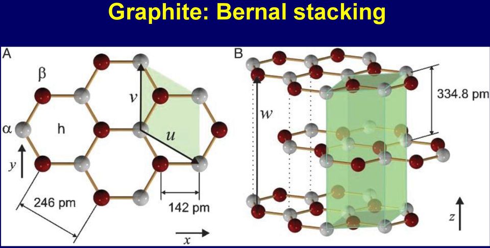
19 Atomic-scale contrast: maxima on the atoms honeycomb image STM Experiments: bright protrusions form an hexagonal lattice!!

20 Low-bias STM: Imaging of the β sublattice A I( ) I( ) I( ) I( ) * Experiments: contact resistance data * Theory: Calculations for tip-surface distance= 0.5 and 1 Å D. Tomanek et al., Phys. Rev. B 35, 7790 (1987).

21 Atomic-scale contrast: honeycomb vs hexagonal
22 Atomic-scale contrast: maxima on the atoms or hollow sites? honeycomb hexagonal hexagonal STM images taken with very different operation conditions and bias voltages show always an hexagonal symmetry
 *Hölscher et")
23 Force F short / nn SPM on low dimension carbon materials STM: Graphite (>25 years ago) FM-AFM (>10 years): Graphite o Albers et al, Nature Nano 2009; Hembacher et al, PRL 2005; Hembacher et al, PNAS 2003; Hölscher et al, PRB 2000; Carbon Nanotubes o Ashino et al, PRL 2004; Ashino et al nanotech 2005; PAHs: Pentacene o Gross et al, Science 2009 *Cisternas et al, PRB 79, (2009) *Hölscher et al, PRB 62, 6967 (2000) *Hembacher et al, PNAS 100, (2003) 0,00-0,03-0,06-0,09-0,12 *Ashino et al, Nanotec. 16, S134 (2005) -0,15 0,3 0,4 0,5 0,6 0,7 Distance z / nm
24 Imaging nanotubes with FM-AFM M. Ashino et al, Phys. Rev. Lett. 93, (2004). M. Ashino et al., Nat. Nanotechnol. 3, 337 (2008).


25 Frequency Shift vs Distance Individual Atomic Lattice Sites Frequency Shift f / Hz H Distance z / nm Frequency Shift f / Hz H -70 dark bright Distance z / nm M. Ashino H. Hölscher et al., PRB 62, 6967 (2000).
26 Force F total / nn Force F short / nn Analysis of Short-Range F short (z) Curves 0,00 Total Forces F total 0,00 Short-Range Force F short -0,05-0,10 F long z B z off, long -0,05-0,10 0,00-0,15-0,20-0,25 0,0 0,5 1,0 1,5 2,0 2,5 3,0 H Distance z / nm H -0,15-0,20-0,05-0,10-0,15 0,2 0,4 0,6 0,8-0,25 0,0 0,5 1,0 1,5 2,0 2,5 3,0 Distance z / nm F short = F total F long * ) *) Guggisberg et al., PRB 61, (2000). Si(111)-7x7 ** ) M. Ashino **) M. Lantz et al., Science 291, 2580 (2001).

 E 0 (C1) 87.4 mev E 0 (C2) 91.")
27 Force F short / nn Analysis of Short-Range F short (z) Curves 0,00 Forces derived from Lennard-Jones Potential -0,03-0,06 F L J z 12E z 0 0 z z 0 13 z z 0 7-0,09-0,12-0,15 0,3 0,4 0,5 0,6 0,7 Distance z / nm Tip H E 0 = Binding Energy z 0 = Equilibrium Distance ( z nm ) E 0 (C1) 87.4 mev E 0 (C2) 91.8 mev E 0 ( H ) 101 mev M. Ashino
28 77.f.top / 19/11/09 Origin of the atomic contrast? FM-AFM: DFT+vdW Forces on SWCNT and graphite (0001) Is vdw providing atomic resolution? atomic contrast versus tip reactivity Does STM always image atoms?: multiple scattering effects Graphene on Pt(111): Moire patterns Vacancies on Gr/Pt(111): Are the localized states on the vacancy preserved? 5.2Å 6K M. M. Ugeda et al, PRL 104, (2010)
. o Semiconductor.")
29 DFT+vdW calculations on CNT: system Nanotube (17,0) o Similar diameter to the NT used in experiments (1,34 nm vs 1,38 nm). o Semiconductor. o Small unit cell H 1,28 nm Unit cell: 204 atoms 1,34 nm
30 DFT+vdW calculations on CNT: Tips CHEMICAL REACTIVITY O apex atom in a Si tip Dimer Si tip H3 Si tip Metallic W tip
31 DFT+vdW calculations on NT: method Atomistic simulations with DFT + vdw: DFT calculation: o VASP: PW + PAW pseudopotentials o Electronic exchange correlation: PBE (also LDA) o Supercell calculation, 1x4x1 Monkhorst Pack (MP) E k -sampling mesh. Convergence criteria: Ecut = 500 ev. Forces < 0.01 ev/å vdw calculation: o Grimme approach [S. Grimme, J. Comp. Chem., (2004)] o Atomic relaxations included o Calculation taking into account the Tip and a large NT fragment (not supercell approach) E TOTAL = E DFT + E vdw

32 Rubén Pérez Forces and Currents on Low-dimensional Carbon Materials. SPM Theory & Nanomechanics Group, UAM DFT+vdW calculations on NT: method Supercell for DFT vs nanotube + single tip for vdw DFT vdw
33 Force (nn) Force (nn) DFT+vdW calculations on NT: Results Dimer Si tip 0,3 0,2 0,1 Difference due to elastic deformation of tip&nt Experiment, SR Force, NT Leonard-Jones fit Ashino et al Nature Nano 2008 Forces vs experiments: GGA gives very small forces GGA+vdW yields the correct order of magnitude ~ nn, but forces are larger than the experimental values, < 0.15 nn (tip model or vdw parameters?). 0,0-0,1-0,2-0,3-0,4-0,5 H, GGA+VdW C, GGA+VdW H, GGA C, GGA H, LDA C, LDA H, VdW C, VdW Tip-NT Distance (Å) LDA provides a surprisingly good agreement with GGA+vdW
 -0,09 Similar behaviour in experiments H -0,12 0,2 0,1 0,0-0,1-0,2-0,3-0,4-0,5")
34 Force F short / nn Force (nn) DFT+vdW calculations on NT: Results Dimer Si tip 0,3 Atomic contrast H or C?: 0,00 H position gives larger forces -0,03 until very small tip-nt distances (bright -0,06 spot in topographic images) -0,09 Similar behaviour in experiments H -0,12 0,2 0,1 0,0-0,1-0,2-0,3-0,4-0,5 H, GGA+VdW C, GGA+VdW H, GGA C, GGA H, LDA C, LDA H, VdW C, VdW Tip-NT Distance (Å) -0,15 M. Ashino 0,3 0,4 0,5 0,6 0,7 Distance z / nm
 Very large Forces -0,3-0,4-0,5-0,6-0,7 H, GGA+VdW C, GGA+VdW H, GGA C, GGA H, LDA C, LDA H, VdW C, VdW 2 3 4 5")
35 Force (nn) DFT+vdW calculations on NT: H3 Si tip H3 Si tip 0,1 0,0-0,1-0,2 Formation of a Si C bond Atomic contrast H or C?: H3 tip is more reactive. C gives larger forces (bright spot in topographic images) Very large Forces -0,3-0,4-0,5-0,6-0,7 H, GGA+VdW C, GGA+VdW H, GGA C, GGA H, LDA C, LDA H, VdW C, VdW Tip-NT Distance (Å)
 larger attractive forces on the hollow site:")

36 Atomic contrast vs tip reactivity For weakly reactive tips, vdw sets the absolute force scale but atomic contrast is always controlled by SR Chemical forces Weakly reactive tips: Pauli repulsion (smaller on areas of low electronic density) larger attractive forces on the hollow site: hexagonal pattern of bright spots Strongly interacting Tip: attractive interaction dominates larger forces on atoms (local change of hybridization) honeycomb pattern Inverted contrast on the repulsive regime M. Ondracek et al, Phys. Rev. Lett. 106 (2011) (Editors Suggestion, 29/04/2011 & ViewPoint)
37 The Chemical Structure of a Molecule Resolved by FM-AFM with a CO tip!! L. Gross et al, Science 325, 1110 (2009)
38 Does STM provides a clear identification of the maxima? STM AFM Hembacher et al, PRL 2005; Hembacher et al, PNAS 2003;
39 STM Simulations: KELDYSH-GREEN S FUNCTION METHOD Exact solution to all orders in the tip-sample hoppings!! I tunnel 4 e / Trace T eff eff ˆ Tˆ f ( ) f TS ˆ SS ST ˆ TT T S d Tˆ eff TS R R 1 1 Gˆ SSTˆ STG ˆ TTTˆ TS Tˆ TS Tˆ TS Tˆ TS Gˆ R SS Tˆ ST Gˆ R TT Tˆ TS... R G TT ( ) R G TT ( ) R G TT ( ) T TS T TS T ST T T TS T ST T TS T ST T + TS + TS +... R G SS ( ) R R G ( ) ( ) SS G SS JM. Blanco, F. Flores and R. P., Progress in Surface Science 81, (2006)


40 W(100) Static STM: results constant height; 1024 k-points, V bias = -0.3 V change in the contrast with the distance inverted contrast for distances < 4 Å due to the multiple scattering effect α Η β α
41 Conclusions: Are we imaging atoms? FM-AFM: The atomic contrast is controlled by the Short Range Chemical forces. vdw interaction sets the absolute force scale. Topographic images yield bright spots on H or C positions depending on the Tip apex: less reactive tips favours the hollow position, more reactive apexes or metallic tips would yield the C atoms as bright spots. STM contrast changes with distance: Bright spots located on hollow sites for close distances. Multiple Scattering required!. AFM is an excellent experimental tool to check the theoretical vdw approaches!
42 Origin of the atomic contrast? FM-AFM: DFT+vdW Forces on SWCNT and graphite (0001) Is vdw providing atomic resolution? atomic contrast versus tip reactivity Does STM always image atoms?: multiple scattering effects Graphene on Pt(111): Moire patterns Vacancies on Gr/Pt(111): Are the localized states on the vacancy preserved? 5.2Å 77.f.top / 19/11/09 6K M. M. Ugeda et al, PRL 104, (2010)
 for a review Macroscopic-sized graphene films recently transferred to arbitrary substrates S. Bae et al., Nature Nano. 5, 574 (2010).")
43 Graphene on metals Highly perfect graphene sheets can be grown on various metals ML graphene on: Co, Ni, Ru, Rh, Pd, Ir, Pt, Cu see J. Wintterlin et al., Surf. Sci. 603, 1841 (2009) for a review Macroscopic-sized graphene films recently transferred to arbitrary substrates S. Bae et al., Nature Nano. 5, 574 (2010). How does the presence of a metallic substrate modify the properties of an The interaction of graphene layers with the different metallic substrates is strongly depending on the metal itself. atomically tailored graphene layer G. Giovannetti et al., PRL (2008). A. B. Preobrajenski et al. PRB 78, (2008) In the weakly interacting systems the electronic structure of ideal graphene is basically preserved. G/Ir(111) G/Pt(111) I. Pletikosic et al., PRL (2009) P. Sutter, et al PRB 80 (2009)
 P. Sutter, et al.")
44 Pristine graphene adsorbed on Pt(111) surfaces Graphene monolayer adsorbed on Pt(111) one of the weakest interacting graphene-metal systems v F = 10 6 m/s A. B. Preobrajenski et al. PRB 78, (2008) P. Sutter, et al., PRB 80, (2009).
 Pt(111) surface (a=2.78 Å) 3x3 1 2 Various moirés patterns are formed T. A. Land et al., Surf. Sci. 264 261 (1992). M. Enachescuet al., Phys. Rev. B 60, 16913 (1999). P. Sutter, et al., PRB.")
45 Pristine graphene adsorbed on Pt(111) surfaces Formed by chemical vapor deposition of ethylene in UHV at temperatures above 1275K ( 21 21)R11º Moiré periodicity ML Graphene (a=2.46 Å) Pt(111) surface (a=2.78 Å) 3x3 1 2 Various moirés patterns are formed T. A. Land et al., Surf. Sci (1992). M. Enachescuet al., Phys. Rev. B 60, (1999). P. Sutter, et al., PRB. B 80, (2009). G. Otero et al. Phys. Rev. Lett. 105, (2010). Our results are basically independent of the moiré superstructure => 3x3 =19.1º

. P. Sutter, et al PRB 80, 245411,(2009)")
46 d//dv (a.u) Pristine graphene adsorbed on Pt(111) surfaces 3x3 moiré ( 21 21)R11º =19.1º 3x Experimental LDOS E D +300meV Bias (V) Dirac point at +300 mev In agreement with theoretical predictions and photoemission estimations G. Giovannetti et al., PRL (2008). P. Sutter, et al PRB 80, ,(2009)
47 d//dv (a.u) Graphene on Pt(111): DFT calculations ( 21 21)R11º 3x3 moiré 3.35 Å Optimal Pt graphene distance!! Theory 0.50 Experiment Experimental LDOS E D +300meV 0.25 Calculation details: DFT- VASP code PBE functional + van der Waals interactions Planewave cutoff: 400 ev STM images: OpenMX code Bias (V) STM corrugation can be explained as a purely electronic effect Calculations reinforce the association of the dip in the DOS with E D position
48 Graphene on Pt(111): STM Graphene on metals: Moiré structures: Topographic or purely electronic effect? Flat graphene layer: corrugation of ~0.03 Å 5.2Å 77.f.top / 19/11/09 6K 0.03 Å 0.00 Å
- (dzx-dzy) W(100)- (spd) 2,129E-9 2,13 na 2,126E-9 2,123E-9 2,121E-9 2,118E-9 2,115E-9 2,113E-9 2,110E-9 2,107E-9 2,105E-9 2,102E-9 2,099E-9 2,097E-9 2,094E-9 2,091E-9 2,089E-9 2,086E-9")

49 Graphene on Pt(111): STM Moiré structures: ANTICORRUGATION!!! electronic effects dominate... Pt(111)- (dzx-dzy) W(100)- (spd) 2,129E-9 2,13 na 2,126E-9 2,123E-9 2,121E-9 2,118E-9 2,115E-9 2,113E-9 2,110E-9 2,107E-9 2,105E-9 2,102E-9 2,099E-9 2,097E-9 2,094E-9 2,091E-9 2,089E-9 2,086E-9 2,083E-9 2,081E-9 2,078E-9 2,07 na 2,075E-9 2,129E-9 2,126E-9 2,123E-9 2,121E-9 2,118E-9 2,115E-9 2,113E-9 2,110E-9 2,107E-9 2,105E-9 2,102E-9 2,099E-9 2,097E-9 2,094E-9 2,091E-9 2,089E-9 2,086E-9 2,083E-9 2,081E-9 2,078E-9 2,075E-9 35,7 na 36,3 na 3,631E-8 3,629E-8 3,626E-8 3,623E-8 3,620E-8 3,617E-8 3,614E-8 3,611E-8 3,608E-8 3,605E-8 3,603E-8 3,600E-8 3,597E-8 3,594E-8 3,591E-8 3,588E-8 3,585E-8 3,582E-8 3,579E-8 3,576E-8 3,574E-8 3,631E-8 3,629E-8 3,626E-8 3,623E-8 3,620E-8 3,617E-8 3,614E-8 3,611E-8 3,608E-8 3,605E-8 3,603E-8 3,600E-8 3,597E-8 3,594E-8 3,591E-8 3,588E-8 3,585E-8 3,582E-8 3,579E-8 3,576E-8 3,574E-8 0,106 na 0,102 na Pt(111)-C- (pz)
50 Vacancies on Graphene/Pt(111) Creation of single vacancies by Ar + irradiation at RT (same parameters as in HOPG)
51 Vacancies on Graphene/Pt(111) Creation of single vacancies by Ar + irradiation at RT (same parameters as in HOPG)
52 Vacancies on Graphene/Pt(111) 4.8 Å 4.8 Å Almost identical features showing non trivial pattern of high LDOS intensity 2.5 nm 4.8 Å 4.8 Å Single C vacancies in HOPG We need bring into play DFT calculations in order to unravel its nature
 (6x6) 1.84 Å 2.")

53 Vacancies on Graphene/Pt(111) Free standing graphene (6x6) 1.95 Å Graphene on Pt(111) (6x6) 1.84 Å 2.90 Å Calculations show a magnetic moment for vacancy in FSG in agreement with O. Yazyev et al, Phys. Rev. B. 75, (2007) Graphene interaction with the metal strongly increases due to vacancies, giving rise to the quenching of the magnetic moment of the system
54 2.77 A Vacancies on Graphene/Pt(111) 1.84 Å supercell with 2 2 units of the 3x3 moiré 2.90 Å Calculations show that each of the bright features found 4.1 Å in the STM images after the ion bombardment is due a Experimental missing C atom 4.11 A 2.8 Å
55 d//dv (a.u) d//dv (a.u) d//dv (a.u) Tunneling Spectroscopy 0.6 LDOS C vacancy LDOS graphene/pt(111) Bias (mv) Even in weakly coupled graphene/metal systems, di/dv measured consecutively at 5K the presence Lock-In parameters: V mod of = 1mV; f = 2.3kHz nm topography Bias (V) the metal has to be seriously taken into account in order to di/dv map at +500mV controllably tune graphene properties by locally modifying its structure LDOS 2.25 V V High Low
56 Quenching of the magnetism (1): doping The doping effect induced by the metal pushes the C π states of both spins above the Fermi level!! A planar structure, like the one of the vacancy in isolated graphene, would be still magnetic!!
57 Quenching of the magnetism (2): relaxation of the unpaired C atom out of graphene plane 0.1 ev above magnetic GS The outward displacement mixes the σ and π states and changes the hybridization of the atom
58 Quenching of magnetism: Gr/Pt(111)
59 Character of the DOS resonance above E F Vacancy on Graphene Vacancy on Gr/Pt(111) The PDOS has esentially a p-character in this energy range
60 Conclusions 1. Forces & Transport in Nanostructures with ab initio methods: a perfect tool to extract information from STM and AFM experiments 2. FM-AFM: single-atom imaging, manipulation, and chemical identification on all kind of surfaces. 3. Forces and currents in carbon nanostructures AFM contrast controlled by tip apex reactivity STM contrast depends on distance: inversion!! Graphene/Pt(111): interaction modifies significantly the properties of the defects 4. Heterofullerenes from planar precursors: Atomic-scale Origami (2D chemistry+ surface catalyzed cyclization) Same ideas applied to the production of graphene nanoribbons (Jao et al., Nature 458, 877 (2010))
61 Acknowledgements THEORY: SPM-TH Group, UAM, Spain M. Ondracek, P. Jelinek (FZU, CAS, Prague), Cesar Gonzalez (ICMM-CSIC) EXPERIMENTS: FM-AFM: Osaka University & NIMS (Tsukuba), Japan: N. Oyabu, Y. Sugimoto, M. Abe, S. Morita & O. Custance Gr/Pt(111): M. M. Ugeda, I. Brihuega, A.J. Martinez-Galera, and J. M. Gómez-Rodríguez (UAM) FULLERENES: ICMM (CSIC): G. Otero,C. Sanchez-Sanchez, R. Caillard, M.F. Lopez, C. Rogero, F.J. Palomares, J. Mendez, J.A. Martin-Gago Chemistry ICMM: B. Gomez-Lor ICIQ: N. Cabello, A.M. Echevarren


62 Scanning Probe Microscopy Theory & Nanomechanics Group SPM-TH Group Leader: Prof. Rubén Pérez Postdoctoral Researchers: o Pablo Pou (RyC) o Delia Fernández o Milica Todorovic PhD Students: o Giulio Biddau o Carlos Gómez o Lucía Rodrigo
63 Acknowledgements & Funding MEC (Spain): Projects MAT , NAN C10-07 EU FP-6: STREP project FORCETOOL (NMP4-CT ) MICINN (Spain): Projects MAT NAN, MAT E (FANAS EUROCORES, ESF), MAT E (NSF Materials World Network) Spanish Supercomputing Network (RES): Magerit (CesViMa, Madrid) & Mare Nostrum (BSC, Barcelona) Thank you for your attention!!
7/3/2014. Introduction to Atomic Force Microscope. Introduction to Scanning Force Microscope. Invention of Atomic Force Microscope (AFM)
") Introduction to Atomic Force Microscope Introduction to Scanning Force Microscope Not that kind of atomic Tien Ming Chuang ( 莊 天 明 ) Institute of Physics, Academia Sinica Tien Ming Chuang ( 莊 天 明 ) Institute
Introduction to Atomic Force Microscope Introduction to Scanning Force Microscope Not that kind of atomic Tien Ming Chuang ( 莊 天 明 ) Institute of Physics, Academia Sinica Tien Ming Chuang ( 莊 天 明 ) Institute
Lecture 6 Scanning Tunneling Microscopy (STM) General components of STM; Tunneling current; Feedback system; Tip --- the probe.
 General components of STM; Tunneling current; Feedback system; Tip --- the probe.") Lecture 6 Scanning Tunneling Microscopy (STM) General components of STM; Tunneling current; Feedback system; Tip --- the probe. Brief Overview of STM Inventors of STM The Nobel Prize in Physics 1986 Nobel
Lecture 6 Scanning Tunneling Microscopy (STM) General components of STM; Tunneling current; Feedback system; Tip --- the probe. Brief Overview of STM Inventors of STM The Nobel Prize in Physics 1986 Nobel
STM and AFM Tutorial. Katie Mitchell January 20, 2010
 STM and AFM Tutorial Katie Mitchell January 20, 2010 Overview Scanning Probe Microscopes Scanning Tunneling Microscopy (STM) Atomic Force Microscopy (AFM) Contact AFM Non-contact AFM RHK UHV350 AFM/STM
Microscopie à champs proche: et application
 Microscopie à champs proche: Théorie et application STM, effet tunnel et applications AFM, interactions et applications im2np, Giens 2010 Optical microscopy: resolution limit resolution limit: d min =
Scanning Tunneling Microscopy: Fundamentals and Applications
 McGill University, Montreal, March 30 th 2007 Scanning Tunneling Microscopy: Fundamentals and Applications Federico Rosei Canada Research Chair in Nanostructured Organic and Inorganic Materials Énergie,
Surface Analysis with STM and AFM
 Sergei N. Magonov, Myung-Hwan Whangbo Surface Analysis with STM and AFM Experimental and Theoretical Aspects of Image Analysis VCH Weinheim New York Basel Cambridge Tokyo Preface V 1 Introduction 1 1.1
What is Nanophysics: Survey of Course Topics. Branislav K. Nikolić
 What is Nanophysics: Survey of Course Topics Branislav K. Nikolić Department of Physics and Astronomy, University of Delaware, Newark, DE 19716, U.S.A. http://wiki.physics.udel.edu/phys824 Definition of
XCVII Congresso Nazionale
 XCVII Congresso Nazionale The Fe(001)-p(1x1)O surface: scanning tunneling microscopy (STM) results and related issues Lamberto Duò CNISM - Dipartimento di Fisica Politecnico di Milano Oxides and thin (few
Microscopie à force atomique: Le mode noncontact
 Microscopie à force atomique: Le mode noncontact Clemens Barth barth@crmcn.univ-mrs.fr CRMCN-CNRS, Campus de Lumny, Case 913, 13288 Marseille Cedex09, France La Londe les Maures (France) -- 20-21/03/2007
Physical Properties and Functionalization of Low-Dimensional Materials
 Physical Properties and Functionalization of Low-Dimensional Materials Physics Department, University of Trieste Graduate School of Physics, XXVI cycle Supervisor: Co-supervisor: Prof. Alessandro BARALDI
Lecture 4 Scanning Probe Microscopy (SPM)
") Lecture 4 Scanning Probe Microscopy (SPM) General components of SPM; Tip --- the probe; Cantilever --- the indicator of the tip; Tip-sample interaction --- the feedback system; Scanner --- piezoelectric
Lecture 4 Scanning Probe Microscopy (SPM) General components of SPM; Tip --- the probe; Cantilever --- the indicator of the tip; Tip-sample interaction --- the feedback system; Scanner --- piezoelectric
The influence of graphene curvature on hydrogen adsorption. Sarah Goler
 The influence of graphene curvature on hydrogen adsorption Sarah Goler Laboratorio NEST, Istituto Nanoscienze CNR and Scuola Normale Superiore, Piazza San Silvestro 12, 56127 Pisa, Italy Center for Nanotechnology
SPM 150 Aarhus with KolibriSensor
 Customied Systems and Solutions Nanostructures and Thin Film Deposition Surface Analysis and Preparation Components Surface Science Applications SPM 150 Aarhus with KolibriSensor Atomic resolution NC-AFM
The Application of Density Functional Theory in Materials Science
 The Application of Density Functional Theory in Materials Science Slide 1 Outline Atomistic Modelling Group at MUL Density Functional Theory Numerical Details HPC Cluster at the MU Leoben Applications
INTRODUCTION TO SCANNING TUNNELING MICROSCOPY
 INTRODUCTION TO SCANNING TUNNELING MICROSCOPY SECOND EDITION C. JULIAN CHEN Department of Applied Physics and Applied Mathematics, Columbia University, New York OXJORD UNIVERSITY PRESS Contents Preface
Usage of Carbon Nanotubes in Scanning Probe Microscopes as Probe. Keywords: Carbon Nanotube, Scanning Probe Microscope
 International Journal of Arts and Sciences 3(1): 18-26 (2009) CD-ROM. ISSN: 1944-6934 InternationalJournal.org Usage of Carbon Nanotubes in Scanning Probe Microscopes as Probe Bedri Onur Kucukyildirim,
Surface-state engineering for interconnects on H-passivated Si(100)
") Surface-state engineering for interconnects on H-passivated Si(100) Roberto Robles, Mikaël Kepenekian, Christian Joaquim, Nicolás Lorente International Workshop on Nanopackaging Grenoble, June 27th 28th,
Surface-state engineering for interconnects on H-passivated Si(100) Roberto Robles, Mikaël Kepenekian, Christian Joaquim, Nicolás Lorente International Workshop on Nanopackaging Grenoble, June 27th 28th,
Electronic transport properties of nano-scale Si films: an ab initio study
 Electronic transport properties of nano-scale Si films: an ab initio study Jesse Maassen, Youqi Ke, Ferdows Zahid and Hong Guo Department of Physics, McGill University, Montreal, Canada Motivation (of
New magnetism of 3d monolayers grown with oxygen surfactant: Experiment vs. ab initio calculations
 New magnetism of 3d monolayers grown with oxygen surfactant: Experiment vs. ab initio calculations 1. Growth and structure 2. Magnetism and MAE 3. Induced magnetism at oxygen Klaus Baberschke Institut
Modification of Graphene Films by Laser-Generated High Energy Particles
 Modification of Graphene Films by Laser-Generated High Energy Particles Elena Stolyarova (Polyakova), Ph.D. ATF Program Advisory and ATF Users Meeting April 2-3, 2009, Berkner Hall, Room B, BNL Department
Spin-flip excitation spectroscopy with STM excitation of allowed transition adds an inelastic contribution (group of Andreas Heinrich, IBM Almaden)
") Magnetism at the atomic scale by Scanning Probe Techniques Kirsten von Bergmann Institute of Applied Physics Magnetism with SPM Spin-polarized scanning tunneling microscopy SP-STM density of states of
Magnetism at the atomic scale by Scanning Probe Techniques Kirsten von Bergmann Institute of Applied Physics Magnetism with SPM Spin-polarized scanning tunneling microscopy SP-STM density of states of
It has long been a goal to achieve higher spatial resolution in optical imaging and
 Nano-optical Imaging using Scattering Scanning Near-field Optical Microscopy Fehmi Yasin, Advisor: Dr. Markus Raschke, Post-doc: Dr. Gregory Andreev, Graduate Student: Benjamin Pollard Department of Physics,
Matter, Materials, Crystal Structure and Bonding. Chris J. Pickard
 Matter, Materials, Crystal Structure and Bonding Chris J. Pickard Why should a theorist care? Where the atoms are determines what they do Where the atoms can be determines what we can do Overview of Structure
SCANNING PROBE MICROSCOPY NANOS-E3 SCHOOL 29/09/2015 An introduction to surface microscopy probes
 SCANNING PROBE MICROSCOPY NANOS-E3 SCHOOL 29/09/2015 An introduction to surface microscopy probes SPM is ubiquitous in modern research Physics Nanotechnology/chemistry Nature Nanotechnology 10, 156 160
Nanoscience Course Descriptions
 Nanoscience Course Descriptions NANO*1000 Introduction to Nanoscience This course introduces students to the emerging field of nanoscience. Its representation in popular culture and journalism will be
Nano-Spectroscopy. Solutions AFM-Raman, TERS, NSOM Chemical imaging at the nanoscale
 Nano-Spectroscopy Solutions AFM-Raman, TERS, NSOM Chemical imaging at the nanoscale Since its introduction in the early 80 s, Scanning Probe Microscopy (SPM) has quickly made nanoscale imaging an affordable
Chapter 8. Low energy ion scattering study of Fe 4 N on Cu(100)
") Low energy ion scattering study of 4 on Cu(1) Chapter 8. Low energy ion scattering study of 4 on Cu(1) 8.1. Introduction For a better understanding of the reconstructed 4 surfaces one would like to know
Low energy ion scattering study of 4 on Cu(1) Chapter 8. Low energy ion scattering study of 4 on Cu(1) 8.1. Introduction For a better understanding of the reconstructed 4 surfaces one would like to know
Scanning Probe Microscopy
 Ernst Meyer Hans Josef Hug Roland Bennewitz Scanning Probe Microscopy The Lab on a Tip With 117 Figures Mß Springer Contents 1 Introduction to Scanning Probe Microscopy f f.1 Overview 2 f.2 Basic Concepts
Nano-Microscopy: Lecture 1. Pavel Zinin HIGP, University of Hawaii, Honolulu, USA
 GG 711: Advanced Techniques in Geophysics and Materials Science Nano-Microscopy: Lecture 1 Scanning Tunneling and Atomic Force Microscopies Principles Pavel Zinin HIGP, University of Hawaii, Honolulu,
Piezoelectric Scanners
 Piezoelectric Scanners Piezoelectric materials are ceramics that change dimensions in response to an applied voltage and conversely, they develop an electrical potential in response to mechanical pressure.
X-Rays and Magnetism From Fundamentals to Nanoscale Dynamics
 X-Rays and Magnetism From Fundamentals to Nanoscale Dynamics Joachim Stöhr Stanford Synchrotron Radiation Laboratory X-rays have come a long way 1895 1993 10 cm 10 µm 100 nm Collaborators: SSRL Stanford:
Section 3: Crystal Binding
 Physics 97 Interatomic forces Section 3: rystal Binding Solids are stable structures, and therefore there exist interactions holding atoms in a crystal together. For example a crystal of sodium chloride
5. Scanning Near-Field Optical Microscopy 5.1. Resolution of conventional optical microscopy
 5. Scanning Near-Field Optical Microscopy 5.1. Resolution of conventional optical microscopy Resolution of optical microscope is limited by diffraction. Light going through an aperture makes diffraction
Exciton dissociation in solar cells:
 Exciton dissociation in solar cells: Xiaoyang Zhu Department of Chemistry University of Minnesota, Minneapolis t (fs) 3h! E, k h! Pc Bi e - 1 Acknowledgement Organic semiconductors: Mutthias Muntwiler,
G raphene layers on metal surfaces have been attracting the attention of scientists since several decades,
 SUBJECT AREAS: SURFACES, INTERFACES AND THIN FILMS ELECTRONIC PROPERTIES AND MATERIALS ELECTRONIC PROPERTIES AND DEVICES SYNTHESIS OF GRAPHENE Received 7 September 2012 Accepted 3 January 2013 Published
STM, LEED and Mass spectrometry
 STM, LEED and Mass spectrometry R. Schloderer, S. Griessl, J. Freund, M. Edelwirth, W.M. Heckl Introduction TDS UHV technique Preparation STM LEED QMS Concept of new UHV chamber Conclusion P. Cole, M.
1 Introduction. 1.1 Historical Perspective
 j1 1 Introduction 1.1 Historical Perspective The invention of scanning probe microscopy is considered one of the major advances in materials science since 1950 [1, 2]. Scanning probe microscopy includes
Atomic Force Microscopy. Long Phan Nanotechnology Summer Series May 15, 2013
 Atomic Force Microscopy Long Phan Nanotechnology Summer Series May 15, 2013 1 World s Smallest Movie 2 Outline What is AFM? How does AFM Work? 3 Modes: Contact mode Non contact mode Tapping mode Imaging
Nanoceanal Spectroscopy of Vibrariums and Electariums
 FEM-Simulationen von Feldverteilungen im elektrischen Rasterkraft-Mikroskop Falk Müller 100 nm 2,93 nm 0 nm Experimental set-up Results Results on gold Application on silicon Numerical umerical simulations
Nondestructive characterization of advanced polymeric materials using spectroscopy and atomic force microscopy
 Nondestructive characterization of advanced polymeric materials using spectroscopy and atomic force microscopy Atomic Force Microscopy Bede Pittenger, Ph. D., Bruker Nano, Santa Barbara, CA Sample Courtesy:
Molecular Dynamics Simulations
 Molecular Dynamics Simulations Yaoquan Tu Division of Theoretical Chemistry and Biology, Royal Institute of Technology (KTH) 2011-06 1 Outline I. Introduction II. Molecular Mechanics Force Field III. Molecular
Scanning Near-Field Optical Microscopy for Measuring Materials Properties at the Nanoscale
 Scanning Near-Field Optical Microscopy for Measuring Materials Properties at the Nanoscale Outline Background Research Design Detection of Near-Field Signal Submonolayer Chemical Sensitivity Conclusions
α Ga (010) α Ga sample is needed to prevent its
 α Ga sample is needed to prevent its") 91 Room temperature STM measurements of α Ga (010) The STM measurements of α Ga (010) in the room temperature phase were performed with the room temperature scanning tunneling microscope described in detail
91 Room temperature STM measurements of α Ga (010) The STM measurements of α Ga (010) in the room temperature phase were performed with the room temperature scanning tunneling microscope described in detail
e - Alessandro Baraldi
 High energy resolution core level photoelectron spectroscopy and diffraction: powerful tools to probe physical and chemical properties of solid surfaces. Alessandro Baraldi e - hν For info, do not hesitate
High flexibility of DNA on short length scales probed by atomic force microscopy
 High flexibility of DNA on short length scales probed by atomic force microscopy Wiggins P. A. et al. Nature Nanotechnology (2006) presented by Anja Schwäger 23.01.2008 Outline Theory/Background Elasticity
Analysis, post-processing and visualization tools
 Analysis, post-processing and visualization tools Javier Junquera Andrei Postnikov Summary of different tools for post-processing and visualization DENCHAR PLRHO DOS, PDOS DOS and PDOS total Fe, d MACROAVE
Lecture 3: Optical Properties of Bulk and Nano. 5 nm
 Lecture 3: Optical Properties of Bulk and Nano 5 nm The Previous Lecture Origin frequency dependence of χ in real materials Lorentz model (harmonic oscillator model) 0 e - n( ) n' n '' n ' = 1 + Nucleus
Chapter 2. Atomic Structure and Interatomic Bonding
 Chapter 2. Atomic Structure and Interatomic Bonding Interatomic Bonding Bonding forces and energies Primary interatomic bonds Secondary bonding Molecules Bonding Forces and Energies Considering the interaction
Near-field scanning optical microscopy (SNOM)
") Adviser: dr. Maja Remškar Institut Jožef Stefan January 2010 1 2 3 4 5 6 Fluorescence Raman and surface enhanced Raman 7 Conventional optical microscopy-limited resolution Two broad classes of techniques
Adviser: dr. Maja Remškar Institut Jožef Stefan January 2010 1 2 3 4 5 6 Fluorescence Raman and surface enhanced Raman 7 Conventional optical microscopy-limited resolution Two broad classes of techniques
Nanoelectronics 09. Atsufumi Hirohata Department of Electronics. Quick Review over the Last Lecture
 Nanoelectronics 09 Atsufumi Hirohata Department of Electronics 12:00 Wednesday, 4/February/2015 (P/L 006) Quick Review over the Last Lecture ( Field effect transistor (FET) ): ( Drain ) current increases
Introduction OLEDs OTFTs OPVC Summary. Organic Electronics. Felix Buth. Walter Schottky Institut, TU München. Joint Advanced Student School 2008
 Felix Buth Joint Advanced Student School 2008 Outline 1 Introduction Difference organic/inorganic semiconductors From molecular orbitals to the molecular crystal 2 Organic Light Emitting Diodes Basic Principals
MOLECULAR DYNAMICS INVESTIGATION OF DEFORMATION RESPONSE OF THIN-FILM METALLIC NANOSTRUCTURES UNDER HEATING
 NANOSYSTEMS: PHYSICS, CHEMISTRY, MATHEMATICS, 2011, 2 (2), P. 76 83 UDC 538.97 MOLECULAR DYNAMICS INVESTIGATION OF DEFORMATION RESPONSE OF THIN-FILM METALLIC NANOSTRUCTURES UNDER HEATING I. S. Konovalenko
Tecniche a scansione di sonda per nanoscopia e nanomanipolazione 2: AFM e derivati
 LS Scienza dei Materiali - a.a. 2008/09 Fisica delle Nanotecnologie part 5.2 Version 7, Nov 2008 Francesco Fuso, tel 0502214305, 0502214293 - fuso@df.unipi.it http://www.df.unipi.it/~fuso/dida Tecniche
Free Electron Fermi Gas (Kittel Ch. 6)
") Free Electron Fermi Gas (Kittel Ch. 6) Role of Electrons in Solids Electrons are responsible for binding of crystals -- they are the glue that hold the nuclei together Types of binding (see next slide)
Free Electron Fermi Gas (Kittel Ch. 6) Role of Electrons in Solids Electrons are responsible for binding of crystals -- they are the glue that hold the nuclei together Types of binding (see next slide)
Experimental Observation of the Quantum Anomalous Hall Effect in a Magnetic Topological Insulator
 Experimental Observation of the Quantum Anomalous Hall Effect in a Magnetic Topological Insulator Chang et al., Science 340, 167 (2013). Joseph Hlevyack, Hu Jin, Mazin Khader, Edward Kim Outline: Introduction:
1 The water molecule and hydrogen bonds in water
 The Physics and Chemistry of Water 1 The water molecule and hydrogen bonds in water Stoichiometric composition H 2 O the average lifetime of a molecule is 1 ms due to proton exchange (catalysed by acids
Scanning Near Field Optical Microscopy: Principle, Instrumentation and Applications
 Scanning Near Field Optical Microscopy: Principle, Instrumentation and Applications Saulius Marcinkevičius Optics, ICT, KTH 1 Outline Optical near field. Principle of scanning near field optical microscope
 g 0 = 3 ev Linear a = 0.246nm. constant velocity g 0 ~ 3 ev 0.334nm Interlayer g 1 ~ 0.4 ev Massive Effective mass: Graphene monolayer-bilayer junction Theoretical studies Nakanishi, Koshino, Ando, PRB
Optical Hyperdoping: Transforming Semiconductor Band Structure for Solar Energy Harvesting
 Optical Hyperdoping: Transforming Semiconductor Band Structure for Solar Energy Harvesting 3G Solar Technologies Multidisciplinary Workshop MRS Spring Meeting San Francisco, CA, 5 April 2010 Michael P.
Surface characterization of oxygen deficient SrTiO 3
 U. Scotti di Uccio Surface characterization of oxygen deficient SrTiO 3 films and single crystals Coherentia-CNR-INFM Napoli, Italy Prof. R. Vaglio R. Di Capua, G. De Luca, M. Radovic, N. Lampis, P. Perna,
Spatially separated excitons in 2D and 1D
 Spatially separated excitons in 2D and 1D David Abergel March 10th, 2015 D.S.L. Abergel 3/10/15 1 / 24 Outline 1 Introduction 2 Spatially separated excitons in 2D The role of disorder 3 Spatially separated
HYDROGEN STORAGE MATERIALS A FIRST-PRINCIPLES STUDY SÜLEYMAN ER ISBN / EAN: 978-90-365-2895-5 DOI: 10.3990/1.9789036528955
 ISBN / EAN: 978-90-365-2895-5 DOI: 10.3990/1.9789036528955 HYDROGEN STORAGE MATERIALS: A FIRST-PRINCIPLES STUDY SÜLEYMAN ER HYDROGEN STORAGE MATERIALS A FIRST-PRINCIPLES STUDY SÜLEYMAN ER HYDROGEN STORAGE
Keysight Technologies How to Choose your MAC Lever. Technical Overview
 Keysight Technologies How to Choose your MAC Lever Technical Overview Introduction Atomic force microscopy (AFM) is a sub-nanometer scale imaging and measurement tool that can be used to determine a sample
Scanning probe microscopy AFM, STM. Near field Scanning Optical Microscopy(NSOM) Scanning probe fabrication
 Scanning probe fabrication") Scanning probe microscopy AFM, STM Near field Scanning Optical Microscopy(NSOM) Scanning probe fabrication Scanning Probe Microscopy 1986 Binning and Rohrer shared Nobel Prize in Physics for invention.stm
Scanning probe microscopy AFM, STM Near field Scanning Optical Microscopy(NSOM) Scanning probe fabrication Scanning Probe Microscopy 1986 Binning and Rohrer shared Nobel Prize in Physics for invention.stm
Etudes in situ et ex situ de multicouches C/FePt
 Etudes in situ et ex situ de multicouches C/FePt : influence de la température sur la structure et les propriétés s magnétiques D. Babonneau, G. Abadias, F. Pailloux Laboratoire de Physique des Matériaux
Highlights of Solid State Physics. Man of the Year Nobel Prizes
 Highlights of Solid State Physics Man of the Year Nobel Prizes Silicon Technology Moore s Law Gordon Moore Intel Jack Kilby 14 nm 2014 Physics Nobel Prize 2000 Integrated Circuit Electrons in the Conduction
Electronic states of disordered grain boundaries in graphene prepared by chemical vapor deposition
 Electronic states of disordered grain boundaries in graphene prepared by chemical vapor deposition Péter Nemes Incze1,2,*, Péter Vancsó1,2, Zoltán Osváth1,3, Géza I. Márk1,2, Xiaozhan Jin2,4, Yong-Sung
Graphene a material for the future
 Graphene a material for the future by Olav Thorsen What is graphene? What is graphene? Simply put, it is a thin layer of pure carbon What is graphene? Simply put, it is a thin layer of pure carbon It has
Phase Characterization of TiO 2 Powder by XRD and TEM
 Kasetsart J. (Nat. Sci.) 42 : 357-361 (28) Phase Characterization of TiO 2 Powder by XRD and TEM Kheamrutai Thamaphat 1 *, Pichet Limsuwan 1 and Boonlaer Ngotawornchai 2 ABSTRACT In this study, the commercial
Photocatalytic and photoelectric properties of cubic Ag 3 PO 4 sub-microcrystals with sharp corners and edges
 Electronic Supplementary Material (ESI) for Chemical Communications Supporting Information for Photocatalytic and photoelectric properties of cubic Ag 3 PO 4 sub-microcrystals with sharp corners and edges
Bi-metallic nanoparticles: A size problem
 Bi-metallic nanoparticles: A size problem Magali Benoit, Nicolas Combe, Hao Tang, Nathalie Tarrat, Joseph Morillo CEMES-CNRS and Université Paul Sabatier, Toulouse, France Toulouse Midi-Pyrénées France
What is molecular dynamics (MD) simulation and how does it work?
 simulation and how does it work?") What is molecular dynamics (MD) simulation and how does it work? A lecture for CHM425/525 Fall 2011 The underlying physical laws necessary for the mathematical theory of a large part of physics and the
What is molecular dynamics (MD) simulation and how does it work? A lecture for CHM425/525 Fall 2011 The underlying physical laws necessary for the mathematical theory of a large part of physics and the
Sampling the Brillouin-zone:
 Sampling the Brillouin-zone: Andreas EICHLER Institut für Materialphysik and Center for Computational Materials Science Universität Wien, Sensengasse 8, A-090 Wien, Austria b-initio ienna ackage imulation
Atomic Force Microscope and Magnetic Force Microscope Background Information
 Atomic Force Microscope and Magnetic Force Microscope Background Information Lego Building Instructions There are several places to find the building instructions for building the Lego models of atomic
Microscopy: Principles and Advances
 Microscopy: Principles and Advances Chandrashekhar V. Kulkarni University of Central Lancashire, Preston, United kingdom May, 2014 University of Ljubljana Academic Background 2005-2008: PhD-Chemical Biology
Vacuum Evaporation Recap
 Sputtering Vacuum Evaporation Recap Use high temperatures at high vacuum to evaporate (eject) atoms or molecules off a material surface. Use ballistic flow to transport them to a substrate and deposit.
A. Ricci, E. Giuri. Materials and Microsystems Laboratory
 Presented at the COMSOL Conference 2009 Milan FSI Analysis of Microcantilevers Vibrating in Fluid Environment Materials and Microsystems Laboratory Politecnico di Torino Outline Brief Presentation of Materials
1. Photon Beam Damage and Charging at Solid Surfaces John H. Thomas III
 1. Photon Beam Damage and Charging at Solid Surfaces John H. Thomas III 1. Introduction............................. 2. Electrostatic Charging of Samples in Photoemission Experiments............................
Università degli Studi di Padova Dipartimento di Fisica e Astronomia Corso di Laurea Magistrale in Fisica
 Università degli Studi di Padova Dipartimento di Fisica e Astronomia Corso di Laurea Magistrale in Fisica SCANNING PROBE MICROSCOPY OF GRAPHENE AND SELF-ASSEMBLED MOLECULES Nicola Galvanetto ANNO ACCADEMICO
BNG 331 Cell-Tissue Material Interactions. Biomaterial Surfaces
 BNG 331 Cell-Tissue Material Interactions Biomaterial Surfaces Course update Updated syllabus Homework 4 due today LBL 5 Friday Schedule for today: Chapter 8 Biomaterial surface characterization Surface
Total Organic Synthesis and Characterization of Graphene Nanoribbons
 Total Organic Synthesis and Characterization of Graphene Nanoribbons Gang Li Seminar in Dong group 03/26/2014 Content History of Graphene Synthesis and Characterization and Properties of Graphene Conceptual
Basic principles and mechanisms of NSOM; Different scanning modes and systems of NSOM; General applications and advantages of NSOM.
 Lecture 16: Near-field Scanning Optical Microscopy (NSOM) Background of NSOM; Basic principles and mechanisms of NSOM; Basic components of a NSOM; Different scanning modes and systems of NSOM; General
Carbon-Carbon bonds: Hybridization
 Carbon-Carbon bonds: Hybridization Abstract: Gina 05/05/11 Molecular binding behavior has a large inuence on the structure of a material and their properties. As a exclusion, carbon bind themself not in
DNA sequencing via transverse transport: possibilities and fundamental issues
 DNA sequencing via transverse transport: possibilities and fundamental issues Massimiliano Di Ventra Department of Physics, University of California, San Diego M. Zwolak and M. Di Ventra, Physical approaches
The self-assembly of metallic nanowires
 Surface Science 600 (2006) L274 L280 Surface Science Letters The self-assembly of metallic nanowires www.elsevier.com/locate/susc J. Schoiswohl a, F. Mittendorfer b, S. Surnev a, M.G. Ramsey a, J.N. Andersen
ATOMIC FORCE MICROSCOPY
 ATOMIC FORCE MICROSCOPY Introduction The atomic force microscope, or AFM, is a member of the family of instruments known as scanning probe microscopes. The AFM operates under a completely different principle
Single Defect Center Scanning Near-Field Optical Microscopy on Graphene
 1 2 3 4 5 6 7 8 9 10 11 12 13 14 15 16 17 Single Defect Center Scanning Near-Field Optical Microscopy on Graphene J. Tisler, T. Oeckinghaus, R. Stöhr, R. Kolesov, F. Reinhard and J. Wrachtrup 3. Institute
Chemical Sputtering. von Kohlenstoff durch Wasserstoff. W. Jacob
 Chemical Sputtering von Kohlenstoff durch Wasserstoff W. Jacob Centre for Interdisciplinary Plasma Science Max-Planck-Institut für Plasmaphysik, 85748 Garching Content: Definitions: Chemical erosion, physical
MBA Lattice Upgrade: New Opportunities for In-situ High Energy (30 kev 90 kev) X-ray Structural Analyses
 X-ray Structural Analyses") MBA Lattice Upgrade: New Opportunities for In-situ High Energy (30 kev 90 kev) X-ray Structural Analyses David Tiede Chemical Sciences and Engineering Division Argonne National Laboratory Workshop on New
MBA Lattice Upgrade: New Opportunities for In-situ High Energy (30 kev 90 kev) X-ray Structural Analyses David Tiede Chemical Sciences and Engineering Division Argonne National Laboratory Workshop on New
Lecture 3: Optical Properties of Bulk and Nano. 5 nm
 Lecture 3: Optical Properties of Bulk and Nano 5 nm First H/W#1 is due Sept. 10 Course Info The Previous Lecture Origin frequency dependence of χ in real materials Lorentz model (harmonic oscillator model)
Modern Construction Materials Prof. Ravindra Gettu Department of Civil Engineering Indian Institute of Technology, Madras
 Modern Construction Materials Prof. Ravindra Gettu Department of Civil Engineering Indian Institute of Technology, Madras Module - 2 Lecture - 2 Part 2 of 2 Review of Atomic Bonding II We will continue
- particle with kinetic energy E strikes a barrier with height U 0 > E and width L. - classically the particle cannot overcome the barrier
 Tunnel Effect: - particle with kinetic energy E strikes a barrier with height U 0 > E and width L - classically the particle cannot overcome the barrier - quantum mechanically the particle can penetrated
Chapter Outline. How do atoms arrange themselves to form solids?
 Chapter Outline How do atoms arrange themselves to form solids? Fundamental concepts and language Unit cells Crystal structures Simple cubic Face-centered cubic Body-centered cubic Hexagonal close-packed
Raman and AFM characterization of carbon nanotube polymer composites Illia Dobryden
 Raman and AFM characterization of carbon nanotube polymer composites Illia Dobryden This project is conducted in High Pressure Spectroscopy Laboratory (Materials Physics group) Supervisor: Professor Alexander
Modification of Pd-H 2 and Pd-D 2 thin films processed by He-Ne laser
 Modification of Pd-H 2 and Pd-D 2 thin films processed by He-Ne laser V.Nassisi #, G.Caretto #, A. Lorusso #, D.Manno %, L.Famà %, G.Buccolieri %, A.Buccolieri %, U.Mastromatteo* # Laboratory of Applied
DO PHYSICS ONLINE FROM QUANTA TO QUARKS QUANTUM (WAVE) MECHANICS
 MECHANICS") DO PHYSICS ONLINE FROM QUANTA TO QUARKS QUANTUM (WAVE) MECHANICS Quantum Mechanics or wave mechanics is the best mathematical theory used today to describe and predict the behaviour of particles and waves.
DO PHYSICS ONLINE FROM QUANTA TO QUARKS QUANTUM (WAVE) MECHANICS Quantum Mechanics or wave mechanics is the best mathematical theory used today to describe and predict the behaviour of particles and waves.
Hydrogen, the simplest and most abundant element in the universe,
 Electric field enhanced hydrogen storage on polarizable materials substrates J. Zhou a,b, Q. Wang c, Q. Sun a,c,1, P. Jena c, and X. S. Chen b a Department of Advanced Materials and Nanotechnology, and
From Quantum to Matter 2006
 From Quantum to Matter 006 Why such a course? Ronald Griessen Vrije Universiteit, Amsterdam AMOLF, May 4, 004 vrije Universiteit amsterdam Why study quantum mechanics? From Quantum to Matter: The main
Explain the ionic bonds, covalent bonds and metallic bonds and give one example for each type of bonds.
 Problem 1 Explain the ionic bonds, covalent bonds and metallic bonds and give one example for each type of bonds. Ionic Bonds Two neutral atoms close to each can undergo an ionization process in order