Contents 1. Introduction 2. Simulation Approach 3. Elementary Circuits
|
|
|
- Allan Briggs
- 8 years ago
- Views:
Transcription
1

2

3 Abstract Physical Unclonable Functions (PUFs) present a promising concept for cryptographic hardware. PUFs provide a challenge-response scheme, where the response is not calculated but determined by a kind of randomness available in the device. Every PUF behaves different, even equally manufactured ones. The Arbiter PUF makes use of race conditions between equally designed delay paths. Although the basic principle is proven to work, it suffers from predictability attacks and a not negligible quantity of unreproducible response bits. This thesis deals with the simulation and enhancement of Arbiter PUFs in CMOS technology. A novel simulation approach is introduced, which allows a reliable prediction of the Arbiter PUF s reproducibility behavior without a transistor level simulation of the whole system. Only the components need to be characterized by circuit simulations using industrial manufacturer models. The resulting PUF can be modeled on a higher level and simulated very fast using statistical distributions. Furthermore the influence of some design parameters on each component s characteristic is investigated. An enhanced parameter set is determined and evaluated using the new simulation approach. Finally the results are verified by transient transistor level simulations for the reference and the enhanced Arbiter PUF. The bit error rate could be reduced by 61 % just by design parameter modifications of specific transistors. III

4

5 Contents 1. Introduction Motivation Properties and Quality Measures Applications Basic PUF Principles Arbiter PUF Construction and Principle Arbiter PUF State Of The Art MOS FET Basics Sources of Variance in Integrated Circuits Outline Simulation Approach Transient Simulation on Transistor Level Mismatch Simulation Noise Simulation Script Control of the Simulator Reducing the Overall Simulation Time Elementary Circuits Inverter Circuit (Logical) Circuit (Transistor Level) Inverter s Typical Slew Rate Inverter s Delay Transmission Gate Transmission Gate Switch Circuit (Logical) Circuit (Implementation) Switch s Delay SR NAND Latch Circuit (Logical) Circuit (Transistor Level) Input Sensitivity (Influence of Noise) Input Bias (Influence of Mismatch) V

6 VI Contents 4. Enhanced Arbiter PUF Components Inverter Influence of Width W on Delay Influence of Width W n on Delay Influence of Width W and C load on Slew Rate Delay Elements in Series Switch Latch Arbiter PUF Simulation and Modelling Composition and Operation Simulation (Transistor Level) Quality Simulation (Component Level) Modeling Delay Elements Modeling Switch Elements Combining Delay and Switch Element Models Modeling Noise in Delay and Switch Elements Modeling Arbiter Model-based Arbiter PUF Simulation Component Level Simulation Results Advantages of Component Level Simulation Proposal of an Arbiter PUF based on Enhanced Components Evaluation of the Proposed Enhanced Arbiter PUF Conclusion and Outlook 57 A. Additional Simulation Results 61 A.1. Inverter Parameter Influence A.2. Switch Parameter Influence A.3. Latch Parameter Influence B. Simulations 65 Abbreviations 67 Selbstständigkeitserklärung 69 Bibliography 7
......................... 48 5.4.1. Modeling Delay Elements........................ 48 5.4.2.")
7 Chapter 1 Introduction 1.1. Motivation Modern cryptographic protocols rely on the secrecy of keys. The algorithms are public. This partitioning is state of the art and it is known as Kerckhoffs s Principle in cryptography. An advantage: Publicly known protocols can be analyzed by everyone, which makes sensible mistakes improbable. What remains is the challenge to keep keys secret. Keys are usually bit strings. Copying is possible, easy, and in general unprovable. Physical Unclonable Functions (PUFs) introduce a functionality which may be utilized for future cryptographic protocols. A PUF is a piece of hardware which transforms an input to an output in a particular way. Usually input and output are bit strings. The mapping from the input to the output depends on some kind of randomness, but the same input should always lead to the same output. The evaluation must be easy while the prediction must be hard, even if complete knowledge of the architecture is available. Thus a PUF provides secret information in a challenge-response procedure, which is illustrated in Figure 1.1. The mapping from a challenge to a response is not done by a mathematical function, where parameters ( keys) are necessary to achieve different mappings, but by some randomness without an external key. randomness challenge PUF response Figure 1.1.: Challenge Response Procedure with PUFs. PUFs generate responses with aid of internal randomness and the external challenge. 1
 introduce a functionality which may be utilized for future cryptographic protocols.")
8 2 1 Introduction What distinguishes a PUF from a key is its unclonability. Applications are conceivable where PUFs could replace secret keys. Again, the protocols and even the hardware design of the PUF can be public. But this time, no key exists which could be shared. All information is random and physically bound to a device. Building and using a PUF are challenging tasks. Up to date both sufficiently reliable constructions and suitable protocols are missing and have to be developed. This thesis deals with the construction of enhanced PUFs in CMOS technology Properties and Quality Measures This section deals with properties which are characteristic or desirable for a PUF. Due to the variety of possible constructions and applications this is a complex but important task. Only a short introduction will be given here. Detailed discussions are available in literature, e.g. in [1]. The following paragraph and enumeration is taken from there. To simplify the property description, we start from a very basic classification for a PUF as a physical challenge-response procedure. Note that already this implicitly assigns two properties to PUFs, i.e. an instantiation of a PUF cannot merely be an abstract concept but it is always (embedded in) a physical entity, and a PUF is a procedure (not strictly a function) with some input-output functionality. [...] For brevity, we use the notation Π : X Y : Π(x) = y to denote the challenge-response functionality of a PUF Π. [...] The informal parts of the property descriptions are clearly marked in sans serif font. 1. Evaluable: given Π and x, it is easy to evaluate y = Π(x). 2. Unique: y = Π(x) contains some information about the identity of the physical entity embedding Π. 3. Reproducible: y = Π(x) is reproducible up to a small error. 4. Unclonable: given Π, it is hard to construct a procedure Γ Π such that x X : Γ(x) Π(x) up to a small error. 5. Unpredictable: given only a set Q = {(x i, y i = Π(x i ))}, it is hard to predict y c Π(x c ) up to a small error, for x c a random challenge such that (x c, ) / Q. 6. One-way: given only y and Π, it is hard to find x such that Π(x) = y. 7. Tamper evident: altering the physical entity embedding Π transforms Π Π such that with high probability x X : Π(x) Π (x), not even up to a small error. Figure 1.2 (taken from [2]) shows some PUF properties including the previously mentioned ones and their relations. Some of them are immediately clear, e.g. that the PUF


9
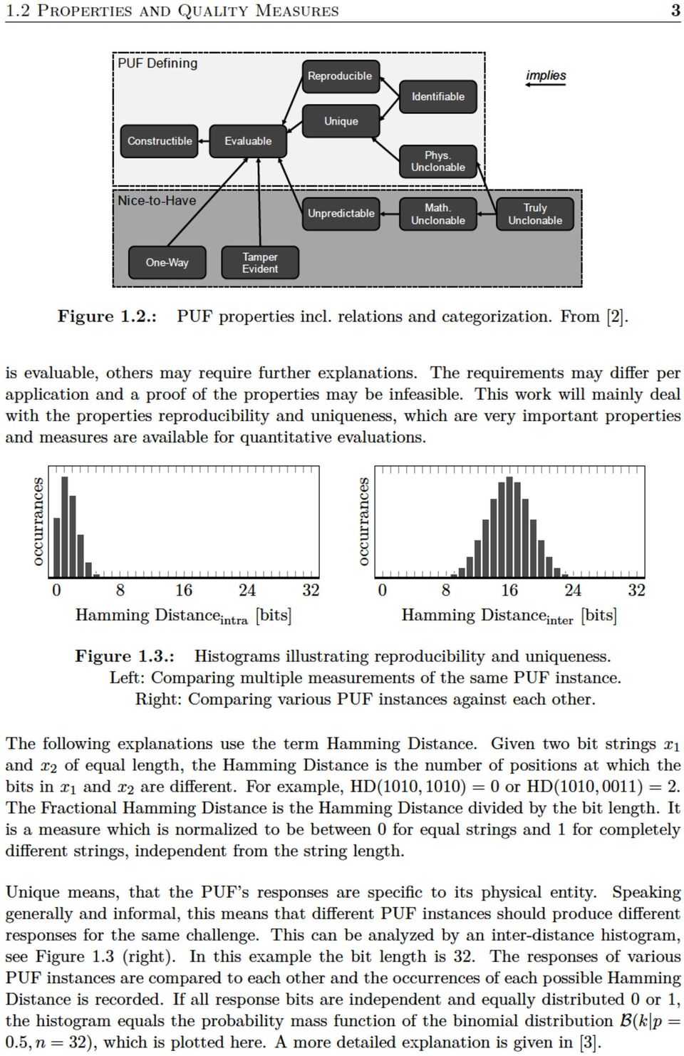
10 4 1 Introduction Reproducible means, that the same challenge on the same PUF instance should always result in the same response. Otherwise said, the response should not depend on noise or environmental conditions. This property can be illustrated by comparing multiple readouts of the same PUF and same challenge. Again, the Hamming Distance can be used to compare the responses and a histogram may look like Figure 1.3 (left). What is shown there is a binomial distribution B(k p =.5, n = 32), which corresponds to a bit error rate of 5 %. Ideally all responses differ by. Although this work has a focus on improving these two aims, other properties are not less important. For example, the common Arbiter PUF which will be introduced in section 1.5 is known to be prone to machine learning attacks [4], which violates the aim for unpredictability Applications Maes et al. [1] make a distinction between three types of application: identification, key generation, and hardware-entangled cryptography. They are briefly introduced below. It was said that PUF responses depend on the challenge, but the mapping is random. Furthermore it is hard to copy a PUF in a way it exposes the same mapping. Thus a PUF can be used to identify a circuit by comparing responses to known responses recorded in advance. Having sufficient challenge-response pairs this method can even authenticate a circuit, this is known as challenge response authentication. For both purposes a small bit error rate can be allowed. No errors are allowed for cryptographic keys, e.g. used for encryption. A PUF can be used to determine a secret cryptographic key, which is used for cryptographic operations. The key can be generated on demand. No permanent storage is needed, from which the key could be leaked. No key programming is necessary, because the key is determined intrinsically. Error correction methods can be applied to allow certain bit error rates in PUF responses and generate correct keys anyhow. Further applications are summarized as hardware-entangled cryptography. An ideal PUF could be modeled as random oracle. A random oracle is a theoretical replacement for a cryptographic hash function. Shortly said, a hash function maps a bit string to a bit string of constant length in a determined way. A cryptographic hash function is a hash function which provides additional properties, e.g. it must be infeasible to generate an input string resulting in a given output string (one way function). Ideal PUFs offer a similar behavior and could thus be applied in cryptographic protocols currently using keyed (parametrized) cryptographic hash functions, e.g. Message Authentication Codes (MAC). It is also possible that PUFs evolve into a new cryptographic primitive, similar to hash functions, which allows the construction of new cryptographic protocols. However, to comply with the requirements such a primitive must provide some challenging properties, e.g. very reliable responses in terms of bit errors, environmental conditions and tamper
, which corresponds to a bit error rate of 5 %. Ideally all responses differ by. Although this work has a focus on improving these two aims, other properties are not less important.")
11 1.4 Basic PUF Principles 5 resilience. A lot of research will be necessary to develop sufficiently good PUFs and PUFoptimized applications. To give an outlook: Gassend et al. propose code, that runs only on a specific processor in 22 [5]. Research on this is is also in progress at the Institute of Distributed Systems at Ulm University Basic PUF Principles There are various ways of implementing a PUF. In literature, mainly two principles are exploited: bi-stability and timing differences. Further constructions and classifications are possible. Constructions are not necessarily electrical. An overview is available in literature, e.g. in [6] or [2], and not given here in detail. An example exploiting bi-stability is the SRAM PUF. It was proposed by Guajardo et al. [7] and Holcomb et al. [8] in 27. An SRAM cell is a simple transistor circuit capable of storing one bit of data. However, after power up the state is undefined. If the power up states of various bits differ, the pattern can be characteristic for a specific device and differ for different devices of the same kind. An example exploiting time differences is the ring oscillator PUF. It is based on delay lines which are connected to act as oscillators. The frequencies of oscillators can be compared to each other. The information which of both oscillators runs faster can be evaluated to a response bit. For different configurations of the oscillators ( challenge) the relation can differ. Due to the equally designed oscillators the responses depend on the specific device and can differ for different devices of the same kind. This idea was already proposed by Gassend et al. [5] in 22. This thesis will deal with the Arbiter PUF, which is another kind of delay based PUF. It was introduced by Lee et al. [9] in 24. Its idea is to introduce a race condition between two equally designed delay paths and decide for the faster one. The construction concept is explained in the next section Arbiter PUF Construction and Principle Lim, Lee, et al. [4] introduced the Arbiter PUF as following: An arbiter-based PUF is composed of delay paths and an arbiter located at the end of the delay paths. [Figure 1.4] depicts an arbiter-based PUF circuit. In this scheme, we excite two delay paths simultaneously and make the transitions race against each other. The arbiter determines which rising edge arrives first and sets its output to or 1 depending on the winner. The circuit takes 64 challenge bits (b i ) as an input to configure the delay paths and generate a 1-bit response as an output.

12 6 1 Introduction Figure 1.4.: Structure of an arbiter-based PUF (basic arbiter scheme). From [4]. The actual implementation of each component will be discussed in chapter 3, an evaluation is given in chapter Arbiter PUF State Of The Art To the best of the author s knowledge no currently known PUF construction is able to provide all desired properties in an acceptable extent for versatile applications. However there are numerous enhancements on each PUF construction improving a certain property. The following overview is limited to Arbiter PUFs, which are examined in this work exclusively. The Arbiter PUF proposed in [9] is prone to violating some of the desired PUF properties. The most severe problems affect reproducibility and unpredictability. The bit error rate is not neglectable, e.g. 3 % for a 64 bit Arbiter PUF in TSMC 65nm technology [2]. Machine learning algorithms can predict responses with small error rates, e.g. 5 % prediction error after only 5 training samples for a 64 bit Arbiter PUF [2]. However, these values differ a lot in literature and the absolute numbers have to be regarded with care. Various countermeasures against predictability were proposed. Lee et al. proposed feed forward paths leading to non-linearities in the delay paths [9]. Majzoobi et al. proposed input and output networks to hide the real PUF behaviour [1]. Rührmair et al. demonstrated attacks on PUFs with and without these protections. It was shown that despite attacks are still possible, the effort in model building and training data increases significantly [11].


13

14 8 1 Introduction is isolated from the rest by a gate oxide (gray), a channel is invoked between source S and drain D. The channel allows current to flow if a voltage U DS > is applied. In the following the source S is fixed to the lowest potential, U S = V. Figure 1.5 (b) displays the corresponding circuit symbol to the bird s view. 1 1 out 1 in 1 (a) (b) (c) Figure 1.6.: (a) nmos inverter circuit. (b)(c) Illustration of the digital inverter functionality. For digital circuits the function can be simplified to a voltage controlled switch, see Figure 1.5 (c). At a low gate voltage the switch is off, for sufficiently high voltages the switch is closed. Exploiting this functionality allows building digital circuits like an inverter, see Figure 1.6 (a). The output is high if the input is low (b), the output is pulled low if the input is high (c). ID [µa] U DS = 1.2 V 5 U th 1.2 U GS [V] ID [µa] linear saturation 5 U GS = 1.2 V 1.2 U DS [V] (a) Input Characteristic (b) Output Characteristic Figure 1.7.: Exemplary transistor input characteristic and output characteristic. The drain current as a function of the gate voltage ( input) and drain voltage ( output). For analog circuits the equivalent model can be expanded to a voltage controlled current source, see Figure 1.5 (d). This is illustrated by the input characteristics, see Figure 1.7 (a). When the gate voltage U G = U GS exceeds the threshold voltage U th, current starts flowing. The higher U G, the higher I D. However, the current I D does not only depend on U GS, but also on U DS, the voltage over the current source, see the output characteristic in Figure 1.7 (b). Only for higher voltages, within the so called saturation region, the current I D is almost independent from U DS and the assumption of a current source is a good one. A circuit exploiting the characteristics is a simple inverting common source amplifier,
.")
15 1.7 MOS FET Basics 9 see Figure 1.8 (a). The conversion of the input voltage to a current is illustrated in Figure 1.8 (b). The resistor transforms the current to the output voltage. In Figure 1.8 (c) an exemplary waveform is given which demonstrates the inverting voltage amplification. The amplification of the transistor can be expressed with aid of the transconductance g m = I D U G. It puts the output current in relation to the input voltage. in out in out voltage [V].7.4 in out 1 2 time [ms] (a) (b) (c) Figure 1.8.: (a) nmos common source amplifier circuit. Illustration of the (b) current source functionality and (c) the inverting amplifier. Each transistor offers at least two design parameters: its width W and length L, see bird s view in Figure 1.5 (a). Not only the pin voltages but also these parameters influence the characteristics, e.g. a larger width W results in higher currents. Good and not too complex approximations determining the current I D in the linear region and saturation region (indicated in Figure 1.7 (b)) are given in Equation 1.1 and 1.2. They are taken from [14] and do not regard any second order effects. ( W I D β n L I D β n 2 U GS U th U DS 2 ) U DS U GS > U th, U DS < U GS U th (1.1) W L (U GS U th ) 2 U GS > U th, U DS > U GS U th (1.2) The constant β n is proportional to the charge carrier mobility. In both regions the current is proportional to W: I D W L. The independence of I D from U DS in saturation region is expressed by the fact that U DS does not appear in Equation 1.2. The size of a transistor also changes its gate capacitance, approximately C G W L. This is relevant because a transistor gate acts as load on a potential previous stage. The behavior of a pmos is basically similar to the nmos, but signs (and constants) are changing, see Figure 1.9. A pmos requires a negative gate voltage U GS and a negative drain voltage U DS to operate. Only these two transistor types are used in this work.
![It puts the output current in relation to the input voltage. in out in out voltage [V].7.4 in out 1 2 time [ms] (a) (b) (c) Figure 1.8.: (a) nmos common source amplifier circuit.](/docs-images/40/1500352/images/page_15.jpg "Illustration of the (b) current source functionality and (c) the inverting amplifier. Each transistor offers at least two design parameters: its width W and length L, see bird s view in Figure 1.")
16 1 1 Introduction U GS G G U GS S D D S U DS (a) nmos U DS (b) pmos Figure 1.9.: Circuit symbol and voltages of (a) nmos transistor and (b) pmos transistor Sources of Variance in Integrated Circuits Manufacturing integrated circuits (ICs) in nanometer scale is a process at technology limits. Structures are only as small as the technology to build them is sufficiently controllable. There are various factors introducing inaccuracies, leading to the fact that every device (transistor or a complete circuit) is a little different from the specification. This is usually unwanted, but indispensable for PUFs. Note that this thesis solely uses standard CMOS technology; materials and processes are not touched. Variance can be explained physically, like uneven thickness of the oxide or uneven doping in the channel. Variance can also be described by consequences, like varying threshold voltage U th or varying constants like β n which includes charge carrier mobility. None of these is further explained here. But a categorization is made and necessary for the next chapters. One has to distinguish between manufacturing variances affecting all devices in the proximity equally (global mismatch, named process variation in the following), and inter device variation even in close proximity (local mismatch, simply named mismatch in the following). The latter is particularly important for our purpose. Even after manufacturing, the behavior of an IC may differ. It can depend on environmental conditions like temperature or supply voltage. Also chip aging was observed [15], making the IC a time variant system. Furthermore, noise is present in each circuit and prevents exploiting too tiny mismatches. All these are unwanted sources of variance and must be kept in mind when building and applying a PUF. There is only a single environmental influence which is allowed to change the PUF behavior: tampering attempts Outline This work deals with enhancements of Arbiter PUFs in order to improve their reliability in terms of reproducibility. Therefore the concept of the Arbiter PUF and all its components are investigated and a profound understanding of its functionality is obtained. All examinations are based on applicable simulations. The thesis is segmented as follows.
 is a little different from the specification.")
17 1.9 Outline 11 A suitable simulation approach is presented in chapter 2. It will be outlined how established simulation tools can be operated to analyze Arbiter PUFs, why this can be effortful, and how time can be saved. This knowledge is absolutely necessary for all following examinations. The components used for Arbiter PUF proposals in literature are analyzed in chapter 3. Implementations known from literature are characterized. It is shown how delay elements and switch elements can be characterized by the distribution of their propagation delay. It is also shown how the arbiter works and which signal and design parameters influence its reliability. The components are improved in chapter 4, by simple measures. The previous chapter delivered valuable knowledge and a reference case to quantify improvements. More deviation is introduced in delay and switch elements, the arbiter is made less noise-sensitive. The components are combined to a complete Arbiter PUF in chapter 5 and measures for the quality are evaluated. The newly designed components are also combined to a PUF and the results are compared. Finally chapter 6 summarizes the achievements and provides ideas for future work.

18

19 Chapter 2 Simulation Approach Manufacturing every integrated circuit analyzed in this work is unfeasible due to its cost, alone in terms of time. Simulations are necessary to predict the behavior of a circuit without manufacturing. This chapter introduces the simulation approach used throughout this work Transient Simulation on Transistor Level Simulating a PUF is not trivial. An analogue circuit simulator is required to perform transient simulations on a transistor level design. Standard CMOS technology is used, for which simulation models and simulators are available. The simulator requires good transistor models which depict the manufactured devices well, especially the mismatch and process variation, and even if devices are used in an uncommon way. The arbiter PUF relies on (small) timing effects and thus requires a simulation of the temporal behavior. This is addressed with a transient simulation. Our simulations make use to the Cadence Virtuoso SPECTRE Circuit Simulator and industrial manufacturer models of TSMC s 9nm technology Mismatch Simulation Mismatch is extremely important for PUFs. It is the reason why PUFs work at all. Thus the transistor models need to provide mismatch information. Unlike some other applications, not only the worst case (corner) is relevant, but a realistic distribution is required. 13

20 14 2 Simulation Approach Monte Carlo (MC) Simulations address this issue. The circuit is not simulated once, but several times. Each time realistic parameters are used for every transistor. The parameters are randomly chosen from a distribution deposited in the models. Thus every transistor, even equally designed ones in the same circuit and same simulation run, has its own behavior. The behavior has to be realistic and as random as after manufacturing. Using a sufficiently high number of MC simulations this allows more general predictions than a single simulation with the nominal parameters. For PUFs a nominal run is senseless anyway, because responses would rely on the simulator accuracy rather than PUF behavior. Various sources of variation were introduced in section 1.8. The simulation environment differentiates between process variation and device mismatch, which can be enabled separately or together. For realistic simulation results of a whole system, it is recommendable to turn both on. However, most of the simulations in this work will not represent a whole system but one of its components. Numerous instances of the simulated component are later combined to a system. In this case process variation should be excluded, because process variation represents global mismatch on the system and may not be regarded for each component separately Noise Simulation Noise is very important to evaluate the PUFs reliability. It is always present in reality and has to be included in the simulations, too. This again adds requirements on the used simulation environment. The chosen simulation environment offers the inclusion of transient noise. However, simulating noise is costly. The computation time for a simulation depends strongly on the noise bandwidth, but a higher noise bandwidth promises more realistic results. This issue will be addressed later in subsection Script Control of the Simulator Uniqueness and Reproducibility are two important PUF properties which were introduced in section 1.2. Analysis of uniqueness requires multiple MC runs. Analysis of reproducibility requires multiple noise runs. These evaluations must take place after every change in the design, even after a single parameter change. And the evaluation may take hours. An environment is required which allows an automation of tasks. It should be flexible enough to allow parameter sweeps and the like. To achieve this aim the genuine simulation can be controlled by a scripting language. The simulations are prepared in the simulation environment, but executed from the script. Parameters can be changed in advance by the script, the evaluation can take place automatically. A very detailed and practice-oriented explanation is present in appendix B.

21 2.5 Reducing the Overall Simulation Time Reducing the Overall Simulation Time The speed of simulations is a limiting factor. Multiple simulations are required for one PUF evaluation, each simulation is costly, mainly due to noise. Running n = 2 MC runs and m = 2 noise runs already results in a total of n m = 4 runs per evaluation. Temperature or parameter sweeps contribute additional factors. In the following a distinction is made between simulated time and simulation time. The evaluation of a PUF response takes some time, even on a manufactured PUF in reality. This evaluation time defines a lower limit for the simulated time. Simulating the same time interval in a circuit simulator takes much longer. This is named simulation time. The simulation time for a certain simulated time interval is necessary and cannot be reduced easily. However, many independent simulations of the same circuit are required. Thus parallelization is possible. Nevertheless it became evident that each simulation produces a huge overhead and most of the time elapses for it. Several actions were taken to reduce the overhead and thus reduce the overall computation time per evaluation. Time for parameter sweeps on MC simulations can be saved if the simulator input (netlist etc.) is reused. The input is equal anyway except for the sweep parameter, and changing the simulation parameter directly before re-triggering the simulator is much faster than generating its complete input again for every run. Time for multiple noise runs can be saved if all runs are done within a single simulation. Instead of starting n simulations of length t with different noise seeds, starting one simulation of length n t avoids the overhead of n-1 runs. Very detailed explanations are present in appendix B. Considering all mentioned simulation enhancement techniques the computation time is reduced significantly without losing accuracy. The importance is demonstrated by an illustration of the time saving in Figure 2.1. Base is a simulation of a demonstration circuit, so the relation of the times is more relevant than the absolute values. Execution time is the time needed to perform 2 MC runs with 2 noise runs each. The reference run performs all 4 simulations sequentially and every run produces overhead. The simulation environment can perform multiple simulations at a time. Therefore only settings need to be adapted, so this is referred to as quick enhancements. Further improvements were introduced in this section which mainly reduce the overhead. Combining all measures is summarized as sophisticated enhancements. For details see appendix B.
22 16 2 Simulation Approach reference run quick enhancements sophisticated enhancements execution time [min] Figure 2.1.: Time savings using enhanced simulation techniques.
23 Chapter 3 Elementary Circuits In this chapter some basic circuits that can be used in a PUF, in particular in an Arbiter PUF, are presented. The Arbiter PUF consists of delay elements, multiplexers, and an arbiter. There are various options for each of these components to be implemented. The ones that will be examined here are: inverters as delay elements, transmission gate multiplexers for choosing a signal path, a latch for deciding on the faster of the two paths Inverter The inverter is a very simple element. Nonetheless it is of great importance for many PUF architectures like the arbiter PUF or the ring oscillator PUF. This is the reason why it is important to understand its function. Although it is a simple element, it already introduces a few design parameters that influence its behavior, namely the sizes of the two involved transistors. We will deal with that later, for the moment we assume minimum size transistors Circuit (Logical) The basic function of an inverter is to negate its input in terms of a HIGH (near VDD) or LOW (near ground) voltage signal. In digital circuits these signal levels correspond to 17
24 18 3 Elementary Circuits in out in 1 out 1 Figure 3.1.: Inverter symbol and truth table. a logical 1 or. Due to the limited options the truth table indicating the static behavior is very simple, see Figure Circuit (Transistor Level) VDD in pmos out nmos DUT in out voltage [V] in out time [ns] (a) (b) (c) Figure 3.2.: (a) CMOS inverter circuit, (b) test circuit, and (c) transient signal. The circuit of the CMOS inverter consists of a pmos and an nmos transistor, see Figure 3.2 (a). A low signal at the input causes the nmos to be off and the pmos to be on which pulls the output high, and vice versa. Assuming a capacitive load no current is necessary to preserve a state. For our application we are mainly interested in the transient behavior, which is of course not ideal. Traversing a rising edge at the input the initially blocking nmos starts conducting more and more (I D ) due to the rising U GS and the pmos in contrast closes. The output node discharges. Due to the transistor characteristics to be passed and the output to be discharged, transitions take some time and edges are not infinitely steep. The path in the test circuit, Figure 3.2 (b), starts with an inverter to get a realistic input for the device under test (DUT) and adds another inverter at the output to simulate a realistic load. Figure 3.2 (c) displays the result of a transient simulation of the test circuit. Note that the regarded in- and output are relative to the single inverter in the middle. Thus the value of the capacitor does not really matter in this setup. The following subsections will establish some measures to characterize the transient behavior.
25 3.1 Inverter 19 voltage [VDD].8.2 t rise t rise t fall Figure 3.3.: Definition of inverter s fall time and rise time Inverter s Typical Slew Rate As previously mentioned the inverter changes its output voltage gradually. This subsection first introduces a measure for the speed: t fall is defined as the time the signal needs to fall from 8 % to 2 % of VDD. t rise is defined respectively, see Figure 3.3. Assuming a linear progression this corresponds to the rise time t rise or the reciprocal slew rate which is usually defined as max( du dt ). As we will mostly deal with delays in our context, the time measure is preferred in this paper. in DUT out voltage VDD 2 time [ps] voltage VDD 1 time [ps] (a) (b) (c) Figure 3.4.: Examination circuit and exemplary waveforms. Figure 3.4 (a) shows a test circuit to analyse t fall of an inverter. The input slew rate is variable, the output node is self loaded which means another inverter is placed there. The signal curves show examples for a fast and a slow rising input edge. Note the different scaling of the time axis. These examples outline clearly that the inverter has a specific transient behavior rather than a logical one. The output voltage at a specific time cannot be calculated by the input voltage at that time. For the fast rising edge, Figure 3.4 (b), the output starts falling below VDD not before the input fully reached VDD. The output slew rate is slower than the input, t fall > t rise. For a slow rising edge, Figure 3.4 (c), the output toggles at about VDD/2 at the input. In this case the output slew rate is faster than the input, t fall < t rise. The transient behavior also makes clear why it was necessary to introduce the artificial measures t fall and t rise. Plotting t fall,out against t rise,in this behavior also becomes evident, see Figure 3.5 (a). For short rise times the output slew rate is almost independent of the input slew rate. For longer rise times it increases, but slowly. This means it makes sense to define a typical
26 2 3 Elementary Circuits tfall,out [ps] t rise,in [ps] trise,out [ps] t fall,in [ps] (a) (b) Figure 3.5.: Behavior of inverter s fall time and rise time. slew rate in an inverter chain (red circle). Within an inverter chain the slew rate where t rise,in = t fall,out will prevail. In this case t fall,typical is 7.2 ps. The same measure can be applied for a falling input edge resulting in a rising output edge. This is shown in Figure 3.5 (b). It is remarkable that t rise,typical, which is 18 ps, is a factor of 2.5 higher than t fall,typical. The typical rising edge is slower than the falling edge. This results from a higher resistance of a same sized pmos transistor due to the lower charge carrier mobility. This is a reason why normal inverters are built with a larger pmos transistor in comparison to the nmos. The gained insight predestines the inverter to refresh edges to a defined slew rate if needed for a subsequent stage. Note that the absolute slew rate is still dependent on the transistor parameters and the load. This will be examined in chapter Inverter s Delay input shaping in DUT out load voltage [V] time [ps] in out Figure 3.6.: Examination circuit and illustration of the typical delay of two inverters in series. This subsections deals with the delay, which is the probably most important property of an inverter in the PUF context. A side effect of the previous subsection is the insight that defining a delay of a single inverter might be difficult. The test circuit in Figure 3.6 addresses this problem by examining an inverter chain. The first inverters are used to generate a realistic input signal, the last inverter serves as a realistic load. By evaluating
27 3.2 Transmission Gate 21 the delay between two inverters instead of one the input and output signal curve are very similar, but delayed. The delay is defined as the time between the input crossing VDD/2 and the output crossing VDD/2. A typical delay value for minimum size transistors in our technology is 32 ps. distribution mismatch noise σ =.17 ps σ = 1.2 ps t [ps] Figure 3.7.: Distribution of the inverter delays. What is even more important than the delay is the deviation of delays. Equally designed transistors will behave differently due to mismatch caused by manufacturing, even when placed near each other in the layout. This issue is addressed by a monte carlo simulation. Figure 3.7 displays the resulting distribution of delays in orange. It shows a standard deviation of 1.2 ps, which is not neglectable in relation to the mean. Another fact that results in varying delays is noise, which causes even a specific manufactured inverter to exhibit slightly different delays every time. This is addressed by simulating transient noise. The resulting distribution is also shown in Figure 3.7 in blue. For our applications it will be important that the deviation introduced by noise is much less than the deviation introduced by manufacturing. Note that the values depend on the transistor parameters, which are minimum size here. Their influence will be examined in chapter Transmission Gate S in S S S out in S S out in on off S R S 1 out R low high (a) (b) (c) Figure 3.8.: Transmission Gate circuit, symbol, and resistance table.
28 22 3 Elementary Circuits A transmission gate is another useful basic element. It acts like a switch and can be turned on and off by an electric signal. Figure 3.8 (a) displays the circuit. It consists of an nmos and a pmos transistor in parallel. For operation two complementary signals S and S are needed. Assuming S is logic high and S is logic low the transmission gate is conducting. The nmos passes logic lows well and the pmos logic highs well. Rather than a digital gate the transmission gate also allows to propagate analog signals. Although its resistance varies with the input voltage, its behavior resembles more a resistor rather than a switch, illustrated in Figure 3.8 (c). Its resistance can be either low or very high, but never zero. The symbol, Figure 3.8 (b), resembles a buffer working in both directions. A detailed introduction and applications can be found at [16, p. 375ff] Transmission Gate Switch An arbiter PUF relies on elements that modify the two signal paths. Each challenge bit (C) stands for a path decision. For this purpose switch elements are needed Circuit (Logical) ina C outa ina C C outa inb outb C inb C outb (a) Figure 3.9.: (b) Switch element symbol and function. A switch element symbol is displayed in Figure 3.9 (a). InA is either propagated to outa or outb; inb to the other output. This behavior is illustrated in Figure 3.9 (b) Circuit (Implementation) The early PUF proposed by Lee et al. in 24 [9] uses transmission gate multiplexers to achieve this. This is illustrated in Figure 3.1 for one output, the same applies to the other
29 3.3 Transmission Gate Switch 23 ina C high ohmic for C=1 outa C C conducting for C=1 inb C Figure 3.1.: Transmission Gate Multiplexer circuit. one (left out for clarity). Inverters at the input drive the transmission gates; inverters at the output load the transmission gate and drive the output node. Figure 3.11.: Switch element path illustrated for C= and C=1. Figure 3.11 shows the two paths and illustrates which circuit elements are affected for both options. It can be assumed that both paths are driven by an inverter of the previous stage (gray) and the output has to drive an inverter of the following stage (gray). Inside, each two corresponding transmission gates are switched on or off in the demonstrated way (black or gray). Note that changing the path is equivalent to interchanging the outputs as long as mismatch is not regarded Switch s Delay Figure 3.12 displays a test circuit to analyze the delay of the switch circuit. Therefore examining one path is sufficient due to the symmetric structure. At the DUT input two inverters have to be driven by a single inverter. The DUT output has to drive a single inverter. Inside the DUT, one path is conducting and the other one is high ohmic. Nevertheless the second path must not be neglected. In a complete switch element the shown circuit exists twice, once per path. Thus a mismatch simulation on the DUT makes sense. A mismatch simulation based on the test circuit in Figure 3.12 will allow statements on the difference of the delays of two paths that are active simultaneously. It is only an
30 24 3 Elementary Circuits in out 1 1 off DUT Figure 3.12.: Switch element delay test circuit. approximation for the comparison of two paths that feed the same output. In this case the second inverter is shared by both paths and only the first inverters and the transmission gates mismatch. Regarding the only two valid switching options illustrated in Figure 3.11 it becomes clear that this case can be neglected in our context, because these paths are never compared directly to each other during operation. distribution mismatch noise σ =.26 ps σ = 1.79 ps distribution mismatch noise σ =.33 ps σ = 2.68 ps rising edge [ps] falling edge [ps] Figure 3.13.: Distribution of the delays of the test circuit. Figure 3.13 depicts the simulation results of the presented switch element test circuit. The propagation of a rising and a falling edge are examined separately because the transmission gates inside the DUT may influence the results differently. As usual we use minimum size transistors. In general the test circuit and the normal inverter chain, which was examined in section 3.1, display similar behavior. Both provide a delay in the range of tens of picoseconds, a mismatch standard deviation in the range of some picoseconds, and a noise standard deviation in the sub picoseconds range. This demonstrates the importance of the switch circuit for the PUF. The switch circuit cannot be neglected and must not be taken for ideal. In the following the switch behavior is analyzed in detail. It is remarkable that a falling edge (Figure 3.13 right plot) progresses slower than a rising edge (Figure 3.13 left plot). And it can be observed that the delay of the falling edge varies far more compared to the rising edge, with a standard deviation of 2.7 ps instead of 1.8 ps, or otherwise expressed
31 3.3 Transmission Gate Switch 25 5 % more. It also turns out that the deviation caused by noise is a bit larger for the falling edge but considering the much higher mismatch deviation it is still in the same range than the corresponding one of the rising edge. The transmission gate was introduced in section 3.2 as a kind of resistor. An investigation is made to check whether the behavior of the transmission gate can be approximated by a resistor to get a simplified model. A modified test circuit is given in Figure The closed transmission gate is replaced by a 1 GΩ resistor, the conducting transmission gate is replaced by a 77 kω resistor. The latter value was chosen to match the mean propagation delay of the unmodified circuit, which is 57 ps for the rising edge. The rising edge was chosen to match, because a rising edge is propagated during the PUF operation. in 77K out 1G DUT Figure 3.14.: Switch element delay test circuit with resistors instead of transmission gates. distribution mismatch noise σ =.3 ps σ = 1.92 ps distribution mismatch noise σ =.29 ps σ = 1.49 ps rising edge [ps] falling edge [ps] Figure 3.15.: Distribution of the delays of the test circuit. Transmission Gates are replaced by resistors. Simulation results for the modified test circuit are displayed in Figure They have to be compared to the results of the original test circuit in Figure The mean delay of the rising edge is equal by design. The deviation of the delay of the rising edge due to mismatch is slightly more than for the original circuit, although the ideal resistor does not introduce additional deviating elements in contrast to the transmission gate. The behavior of the falling edges (right plots in Figure 3.15 and Figure 3.13) differ significantly for both circuits. Neither the mean delay nor the deviation of the delays are similar. This leads to the insight that a simple resistor is not sufficient to approximate the behavior of
32 26 3 Elementary Circuits a transmission gate within the given circuit. Further investigation requires more complex models where for example the voltage dependence of the transmission gate s resistance is regarded. This contradicts the aim for a simple model and is thus not further investigated SR NAND Latch set reset S R Q Q value value Figure 3.16.: SR latch. A latch is a circuit that has two stable states and can thus store 1 bit of information. A latch is not clocked, in contrast to a flip-flop. Figure 3.16 shows the symbol of a set-reset latch (SR latch) with active-low inputs (SR latch). Due to the asynchronous operation the latch can also act as an arbiter. Therefore the two inputs S and R are treated as equal competitors, the output Q indicates which input arrived first. This ability was formerly used in clock synchronization circuits (according to [16, p. 383]) and is very important for arbiter PUFs. The following subsections will deal with the function and some properties of the SR NAND latch, a SR latch built of NAND gates Circuit (Logical) S R Q Q S R Q Q Q Q 1 1 1? 1? keep state set reset forbidden Figure 3.17.: SR NAND latch and truth table. The SR NAND latch consists of two cross-coupled NAND gates, see Figure A NAND gate implements the logic function Y = A B, where Y is the output and A and B are the inputs. Consider the case when R is high and S is low. Forcing S low causes Q to go high. Since R is high and Q is high, the Q output is low. Now consider the case when both S and R are low. Under these circumstances, the latch s outputs are both high. [16]. When operating as storage, this combination is forbidden. It violates the trivial relation Q = Q and the state after releasing S and R simultaneously is not defined. When operating as arbiter, this state is the starting point for a decision due to its instability. Assuming ideal
33 3.4 SR NAND Latch 27 gates, a short delay t between the rising signals at S and R is sufficient to decide for the corresponding stable state which can then be read out safely Circuit (Transistor Level) M2 M3 M6 M7 Q Q Q S M1 R M5 M M4 Q Figure 3.18.: CMOS SR NAND Latch circuit with output buffers. I II III IV Q Q R S time Figure 3.19.: Signal curves representing typical latch applications. Figure 3.18 shows the transistor level circuit of the introduced latch. Its function is based on the two equal NAND gates (M-M3 and M4-M7). Additionally buffers are added to the internal latch outputs (right). Although it could be neglected for simulation, every subsequent circuit using the value of Q or Q loads the latch and may influence the latch s behavior. The given buffers add small loads, too, but they load Q and Q equally. Thus no input is preferred. Unless noted otherwise all transistors are minimum size as usual. Figure 3.19 shows some signal curves to demonstrate the behavior of a latch as arbiter. Each section has a duration of 2 ns.
34 28 3 Elementary Circuits I Pulling S low stores the value 1 in Q and in Q. The visible delay results from the settling time of the latch and the delay of the output buffer. Releasing S keeps the values. II Pulling R low stores the value in Q and 1 in Q. Releasing R keeps the values. III Pulling both S and R low and releasing them exactly at the same time results in an undefined behavior (as long as mismatch is not regarded). Q can settle for 1 or randomly (dotted lines). IV When releasing S and R successively the behavior is again defined (at least as long as mismatch and noise are not regarded): The input released last will dominate and set or reset the value Q. In Section IV the latch acts as arbiter deciding for the order of the input rising edges. This behavior will be explained now in greater detail using the circuit from Figure Starting point is the unstable state where both S and R are low. M3 and M4 are on ( U GS U th ), while M1 and M5 are off ( U GS ). The gates outputs Q and Q are high. Now assume S is rising first. At the left gate M is on and M2 is off because Q =1. Taking M as shorted and neglecting M2 leaves an inverter consisting of M1 and M3. Rising its input lowers its output Q. This affects the right gate where Q is an input. Now M6 is on and M4 closes, which assures that the output Q remains high. This state is now stable even when R is released, too. To achieve reliable decisions for short time differences between the rising edge of S and R it is important that the internal state flips before the second input also arises. Investigations how this behavior can be improved are made in chapter Input Sensitivity (Influence of Noise) S Q R Q t t rise S R V decisions Q=1 [%] t 2 % 1 2 t [ps] (a) (b) (c) Figure 3.2.: (a) Latch test circuit, (b) test input signals, and (c) decision behavior. A manufactured latch is not ideal and one reason for this is noise. This section will deal with the influence of noise on the arbiter decisions. All predictions in this section are
35 3.4 SR NAND Latch 29 based on the Transient Noise Simulation of the SPECTRE Simulator using a Maximum Noise Frequency of 1 GHz. Figure 3.2 (a) shows the test circuit. The input of the latch can be defined arbitrarily. Usually the inputs will resemble inverter edges. For the test the edges are approximated as shown in Figure 3.2 (b). The signals rise linearly from to VDD within a rise time t rise. The interval t between the two inputs is expected to be the most important parameter. V is introduced as the voltage difference between the two signals. Figure 3.2 (c) displays the decision ability of the latch for a given rise time t rise = 1 ps, which is a reasonable. The ideal latch decision function is a kind of sign function. Every t < evaluates to 1, every t > evaluates to, t = is not decidable and should result in a decision rate of 5 %. Unsurprisingly the probability for a correct response decreases in the range around t =. But the image also allows some quantitative proposition. In this case (remember we made assumptions on the input signals and transistor sizes) that means: Avoiding the interval t < 1 ps makes decisions very reliable against the influence of noise. The plot content can be summarized to a single number which allows statements on the quality of the decisions. Therefore t 2 % is introduced. It is defined as the t where 2 % of the runs decide towards Q=1. decisions Q=1 [%] 5 25 t rise = 1 ps t rise = 1 ns.5 1 t [ps] 5 25 t rise = 1 ps t rise = 1 ns 1 2 V [mv] 5 25 t const V const t rise [ps] 5 25 t rise = 1 ps t rise = 1 ns V t [fvs] (a) (b) (c) (d) Figure 3.21.: Influence of test signal parameters on latch decisions. The following investigation demonstrates that t is not the only parameter the arbiter decision is sensitive to. Figure 3.21 (a,b,c) plot the dependence on the three parameters introduced in Figure 3.2 (b). The ideal value for decisions Q=1 is, the worst expectable case is 5 %, which corresponds to a completely random response for Q=1 or Q=. In brief: the lower the better. 2 decisions per data point were evaluated, which is enough for a qualitative statement even if the plots may appear noisy. The blue curve in the t plot Figure 3.21 (a) is exactly what was already shown in Figure 3.2 (c), but only for t >. Due to the symmetric structure of the arbiter it is sufficient to regard one half. The green curve of the same plot reveals the same under the assumption of a longer rise time t rise. It is clearly visible that the decisions become less reliable. For an arbiter this means the inputs would have to differ a lot more in t to achieve the same level of reliability. This is also what the t rise plot Figure 3.2 (c) exposes. The blue curve demonstrates that for an increasing t rise and constant t the rate of false
36 3 3 Elementary Circuits responses increases. This is an important insight: The rise time of the input signals has a big influence on the arbiter behavior. This insight leads to the question what the input is sensitive to instead and if there are better parameters than t. One proposition is V. As can be seen in Figure 3.2 (b) on page 28, V is another kind of distance between the two input signals. The second plot Figure 3.21 (b) examines this proposition. Again the result depends much on t rise. But this time the other way, as the green curve in the third plot Figure 3.21 (c) outlines. For a constant V the false response rate decreases for increasing t rise. This behavior can also be explained regarding the circuit. The inputs always differ by the same voltage, but the rise time corresponds to the time interval the arbiter is exposed to this difference. A longer exposure time increases the chance for the signal to influence the decision in relation to noise. Finally a measure was found to indicate the response rate without direct dependence on the rise time. Figure 3.21 (d) plots the response rate against t V. It is plausible that the two curves indicating different rise times (factor 1) show the same behavior. The recorded data can easily be converted to this format using the relation 3.1 V t = VDD t rise (3.1) decisions Q=1 [%] t [ps] 1 ps sim. 1 ns sim. 1 ns pred. Figure 3.22.: Latch behavior prediction for a different input slew rate. This insight is useful to predict the latch decision behavior in dependence of t for a given rise time, even if the original curve was recorded at another rise time. This saves simulation time because realistic noise simulations are very costly and it was shown before that the rise time influences the behavior significantly. Figure 3.22 extends Figure 3.21 (a) by the prediction (red) of the behavior for t rise = 1 ns based on the values simulated for t rise = 1 ps (blue). The prediction is very similar to the simulated values (green). This underlines that the proposed relation is suitable. The calculation derived from equation 3.1 is developed below. The following calculation converts a latch decision curve recorded at a given rise time to another rise time. Therefore the time value t of each value pair can be converted as following. Knowing a recorded (simulated) value pair ( t rec and its decision rate) it was shown that the product of t and V remains constant (equation 3.2) for varying t rise,
37 3.4 SR NAND Latch 31 and V can easily be calculated using expression 3.1. The final calculation is developed in equations 3.3 below. X = t V = t rec V rec (3.2) t = X V t = X t rise 1 VDD t t t = X t rise VDD X t rise t = ± VDD (3.3) The new value pair consists of the calculated t using the final formula of 3.3 and the unchanged decision rate. There t rise is the rise time which the curve has to be adapted to. The sign of t is the same as the original t rec. decisions Q=1 [%] t [ps] 1 GHz noise 1 GHz noise decisions Q=1 [%] 5 25 t = 1 ps t = 2 ps max. sim. noise [GHz] (a) (b) Figure 3.23.: Influence of noise simulation parameters. Some notes on the noise simulation parameters are attached in the following. The simulation time grows a lot for high maximum noise frequencies to be simulated. Figure 3.23 (a) shows the effect if noise is simulated at reduced maximum noise frequency to save simulation time. At no delay ( t = ) there is almost no difference, both decision rates are around 5 %, which is the ideal value. But at t = 1 ps the decision rate has dropped by half, at t = 2 ps the error seems to have vanished while it is still significant in the more realistic simulation. Figure 3.23 (b) illustrates the error rate in dependence of the maximum noise frequency for the two mentioned ts. It demonstrates that in general using a lower maximum noise frequency results in a illusively lower error rate. But it also demonstrates that the error rate does not change significantly in the range of 1 to 1 GHz. Unfortunately these values may not be valid in general and have to be proven individually. Up to this point the input signals were assumed to be linearly rising edges. Figure 3.24 (a) introduces a more realistic scenario. The inputs are real inverter edges. As it was demonstrated in section 3.1 inverter edges are a bit different, they look smoother and the slew
38 32 3 Elementary Circuits S R Q Q decisions Q=1 [%] pred. sim t [ps] Figure 3.24.: (a) (b) (a) Realistic test circuit and (b) comparison to prediction. rate is intrinsically set. It was outlined that t rise,typical (raise from 2 % to 8 % of VDD) is 18 ps in a minimum size inverter chain, which equivalents a rise time (from to VDD) of about 3 ps. The latch as a load can also be seen as an inverter in this case because every input consists of an nmos and a pmos gate without any extra load. Figure 3.24 (b) compares the predicted decision behavior assuming artificial rising edges at the typical rise time (pred., black) with the decision behavior using realistic edges (sim., red). This is the evidence that the artificial edges, which were introduced to simplify investigations, are a very good model for realistic edges Input Bias (Influence of Mismatch) decision Q=1 yes no distribution σ = 1.45 ps t [ps] latch bias [ps] (a) (b) Figure 3.25.: Decision behavior and distribution of the Bias. The last subsection dealt with the influence of noise. Another artefact that makes decisions unideal results from mismatch. Mismatch causes each transistor to behave slightly different than its specification. Figure 3.25 (a) shows the decision curve for a few different monte carlo runs. The simulation is done without noise. That implies that there is a hard switching point where the arbiter decides for 1 below or for above. It becomes evident that there is a bias in the range of certain picoseconds for these examples and they differ around. Figure 3.25 (b) shows a histogram and a fitted Gaussian distribution for 1 monte carlo runs.
39 3.4 SR NAND Latch 33 It turns out that the bias can be quite significant. For the test circuit a deviation σ of 1.45 ps was calculated. A bias at the arbiter can result in a bias in the PUF response, but it remains unchanged for an arbiter instance at constant environmental conditions. It depends on the application whether the bias has a disturbing effect.
40
41 Chapter 4 Enhanced Arbiter PUF Components This chapter deals with enhancements of the standard Arbiter PUF. Therefore the outlined characteristic properties of its components are taken into account. Every transistor offers design parameters which can be modified at design time. Namely the width W and the length L, which define the size of the transistor, are of interest. More precisely, its deviations given by the manufacturer models and the influence of transient noise are deciding. This leads to the obvious parameter tuning investigation that will be performed in this chapter Inverter The inverter and the inverter chain were introduced as very simple components in section 3.1. Nonetheless every inverter offers a few parameters which can be modified individually: L n : length of the nmos, W n : width of the nmos, L p : length of the pmos, W p : width of the pmos. The supply voltage VDD is also variable. If not noticed otherwise the device under test is an inverter chain consisting of 2 inverters while the parameters refer to all inverters of the complete inverter chain equally, includ- 35
42 36 4 Enhanced Arbiter PUF Components ing previous and following stages. Monte Carlo Variations and Transient Noise are only applied to the devices under test. W without index addresses both W n and W p, the same applies to L. Figure 4.1 (a) displays the test circuit already known from Figure 3.6. The main characteristic property of an inverter chain is its delay. More precisely µ: the mean delay σ mc : the standard deviation of the delay due to mismatch σ noise : the standard deviation of the delay due to noise input shaping in DUT out load examined edge C load (a) (b) Figure 4.1.: Inverter chain s test circuits for (a) delay and (b) edge examination. Furthermore it was outlined that the slew rate is an important characteristic property. It can be expressed by the values t rise : the rise time from 2 % to 8 % of VDD t fall : the fall time from 8 % to 2 % of VDD For the determination of these values a constant load is assumed, see Figure 4.1 (b). A matrix considering the influence of every parameter on every characteristic property was created and is present in the appendix A.1. In the following some outstanding relations are pointed out Influence of Width W on Delay Figure 4.2 displays the influence of the transistor width. µ (left plot) remains more or less constant. This results from the fact that the inverters are loaded by equally sized inverters. This means the load grows equally to the driver strength of the transistors. Much more interesting is the behavior of the deviation, which is illustrated by the standard deviation σ (right plot). The deviation caused by mismatch drops to 48 % for 1 µm devices in
43 4.1 Inverter 37 delay [ps] 6 3 µ σmc [ps] σnoise [ps] W n,w p [nm] W n,w p [nm] Figure 4.2.: Influence of inverter size on delay and its deviation. comparison to the minimum size device. At the first sight this is an unwanted effect. But the deviation caused by noise drops to 33 %. This means the deviation due to noise drops more than the deviation caused by mismatch. Exploiting this effect promises more reliable responses by increasing the transistor size. i i i n C Figure 4.3.: Illustration circuit for inverter operation at a falling edge. The deviation of mismatch behaves as expected. Matching becomes better for larger devices. The behavior of the noise deviation requires further explanation. Therefore a very simple model is used to model the charging procedure within an inverter chain. A current source loads a capacitor, see Figure 4.3. This illustrates an inverter stage (current source) driving another inverter stage (capacitor). The current source is modeled as an ideal current source and a noise current source in parallel. The capacitor voltage is the output signal and is determined by U(t) = 1 t C i( t)d t, assuming C t= =. Splitting the equation to regard the two current sources results in Equation 4.1: t U(t) = 1 C i t + 1 C i n ( t)d t } {{ } noise (4.1) To determine the mean delay the noise term is ignored and the equation is reformed to t = C i U. For increased transistor sizes it can be assumed that C W (gate capacitance goes linearly with W) and i W (drain current goes linearly with W, see Equation 1.1 and 1.2 on page 9). This results in t W W 1, which means the average time to reach a certain voltage is independent from W. To determine the deviation the noise term in Equation 4.1 has to be taken into account, too. The noise current i n is assumed to be Gaussian distributed. Then the integral expresses a
44 38 4 Enhanced Arbiter PUF Components Wiener process. It is typical for a Wiener process that its variance goes linearly with time. In our case this can be ignored because the time was already proven to remain constant in the last paragraph. Also C still behaves like C W. But i n behaves different from i : i n g m i W. The overall impact of W is given in Equation 4.2: σ noise,voltage 1 C i n t 1 W W 1 1 W (4.2) This deviation refers to the voltage over the capacitor. It still has to be transformed to a deviation in time. In this case this is trivial, because is was shown that the slope of the output is independent from W. Thus it can be expressed with Equation 4.3: σ noise σ noise,voltage 1 W (4.3) simulation theory σnoise W n,w p [nm] Figure 4.4.: Evaluation of the theory explaining the noise behavior. The theory is evaluated in Figure 4.4. It can be observed that this result fits the simulation results well, despite the simple model Influence of Width W n on Delay delay [ps] µ σmc [ps] σnoise [ps] W n [nm] W n [nm] Figure 4.5.: Influence of inverters s nmos width on delay and its deviation. Figure 4.5 displays the influence of increasing W n while leaving W p at minimum size. In this case the delay increases (left plot). Regarding the values at 12 nm and 1 µm it
45 4.1 Inverter 39 increases by a factor of 2.4. The influence of mismatch and noise also increases. But for the same parameter change σ mc grows by a factor of 3.3 while σ noise only grows by 1.7. This means the influence of mismatch grows faster than the influence of noise, which makes it desirable to use a larger W n if the increased delay is acceptable. Note that this is contrary to a usual digital inverter design where the pmos is designed larger. nmos i pmos i i n C n C p i i n C n C p i Figure 4.6.: Illustration circuit for asymmetric inverter stage. To explain these observations the examination can be split. Rising and falling edge are regarded separately. The model is extended to depict the fact that only one transistor is increased. Figure 4.6 illustrates this. At first the increase of the delay is described. For the falling edge the nmos determines the current, see the left schematic. In this case i = i nmos W and C = C n + C p C n W. This is almost the same case as before. Current and capacitance grow equally, the time for the falling edge remains approximately constant, t falling 1. For the rising edge the pmos determines the current, see the right schematic. The current remains constant while the load itself grows. It is immediately clear that this results in a slower progress. More precisely, the time t to reach a certain voltage goes linearly with C and thus approximately linear with W n : t rising W n. Thus also the overall delay of the inverter chain increases, although only one edge contributes to that. To explain the noise deviation both edges are regarded separately again. It was outlined in the last paragraph that the falling edge behaves like before, where all transistor sizes were modified. σ noise,falling 1. The noise deviation at the rising edge will be examined now. This case is illustrated on Figure 4.6 (right). An explanation similar to Equation 4.2, which was derived before, is displayed in Equation 4.4: σ noise,rising,voltage 1 C i n t 1 W n 1 W n 1 Wn (4.4) Despite different factors, the result is equivalent to Equation 4.2. Again the result has to be transformed to a deviation in time. This time, the slope varies. It was shown that t rising W n. Regarding this, the deviation in time is expressed in Equation 4.5: σ noise,rising t rising σ noise,rising,voltage W n 1 Wn W n (4.5) Finally the falling and rising edge have to be combined. As known, variances of independent random variables can be added. The resulting relation is given in Equation 4.6: σ noise = σ 2 noise,falling + σ2 noise,rising W n + 1 W n (4.6)
46 4 4 Enhanced Arbiter PUF Components σnoise simulation theory W n [nm] Figure 4.7.: Evaluation of the theory explaining the noise behavior. The predicted behaviour is compared to the simulation in Figure 4.7. Therefore W n from Equation 4.6 is regarded as relative width normalized to W n = 18 nm ˆ= 1. What is still missing is an explanation why the standard deviation due to mismatch increases in the way it does. Therefore rising and falling edge are regarded separately again, see Figure 4.8. It was explained in the beginning of the section that the mean of the falling edge will not change significantly and only the rising edge contributes to its increase. This is proven on the left plot. Nevertheless the standard deviation of the delay of the falling edge increases. µ [ps] complete µ rising edge falling edge σmc [ps] complete σ rising edge falling edge W n [nm] W n [nm] Figure 4.8.: Influence of inverters s nmos width on delay and its deviation. Plotted for rising and falling edge separately. To explain the behavior of the deviation the simple circuit from Figure 4.3 on page 37 is regarded again. There the equation 4.1 for the capacitor voltage was given and solved for t, see equation 4.7: t = C i U (4.7) Both C and i are random variables of a certain distribution. As usual they are assumed Gaussian distributed. For increasing W the distributions will change, in particular the mean of i increases with increasing W of the driver transistor and the mean of C increases with increasing W of the load transistor. While linear operations like addition are easy to perform on such random variables, building a quotient is not. In this case, mean
47 4.1 Inverter 41 and variance cannot be regarded separately any more. Thus both distributions and their behavior for increasing W have to be known completely. Even then the calculations are challenging. As a simplification C is regarded as a constant in the following and only i is assumed a Gaussian distributed random variable. As it appears in the denominator, investigating the influence on t analytically is still not trivial. Even the kind of distribution changes. An illustration is given in Figure 4.9. The figure displays the density function of a Gaussian distributed random variable X and 1 X. It is obvious that the density function 1 of X is not symmetric anymore and assuming a Gaussian Distribution for the result is only an approximation. fx(x) f 1/X (y) x y Figure 4.9.: Illustration of a non-linear operation on the density function of a Gaussian distributed random variable. It was shown that further investigation requires a statistical characterization of i and C and non-linear stochastics to obtain a suitable theoretically well-founded explanation. This effort is not made here. The simulation results provide sufficient information anyhow for the following investigations in this thesis Influence of Width W and C load on Slew Rate time [ps] 5 25 t rise t fall time [ps] 5 25 t rise t fall W n,w p [nm].1 1 C load [ff] Figure 4.1.: Influence of inverter size and load on slew rate. Figure 4.1 shows the main contributors to fast edges. As expected, the transition times decrease with increasing transistor sizes at constant load (left plot), and the transition times increase with increasing capacitive load at constant transistor sizes (right plot). Note that the transition time decreases very slowly for larger transistors while the load affects the transition time almost linearly.
48 42 4 Enhanced Arbiter PUF Components Delay Elements in Series Up to that point a delay element consists of two inverters. The statistical delay behavior for this case was explored. Using the gained delay model allows an easy way to derive the behavior of an inverter chain consisting of 2n (n N) inverters. Assuming independent random variables the overall delay and the standard deviation can be determined by the following equations: µ 2n = n µ (4.8) σ 2n = n σ (4.9) 1 2 n µ2n [µ] n σ2n [σ] n Figure 4.11.: Influence of multiple inverter delay elements in row. This behavior is illustrated in Figure It shows that spending more inverters in a delay chain increases the standard deviation, which is a wanted effect (right plot). But the overall standard deviation grows much slower than the mean (left plot). That means increasing the standard deviation by this measure is very costly in terms of speed and size Switch delay [ps] µ W n,inv [nm] σmc [ps] W n,inv [nm] σnoise [ps] Figure 4.12.: Influence of inverter size on delay of the switch element and its deviation. The switch circuit is analyzed analogously to the delay circuit. All parameter sweeps are available in appendix A.2. Figure 4.12 displays the effect of W n,inv on the delay and its standard deviation. W n,inv is the width of the nmos transistors of the inverters involved in the switch circuit. Transmission gates and pmos sizes remain minimum. The circuit is displayed in Figure 3.12, page 24.
49 4.3 Latch 43 The delay of the switch element behaves similar to the delay of the delay element. The mean delay increases, but the standard deviation due to mismatch increases far more while the standard deviation due to noise hardly changes Latch In subsection the measure t 2 % was introduced which expresses the quality of noise resistance for a latch. It was illustrated in Figure 3.2 on page 28. The less this measure the better is the latch in terms of noise sensitivity. Another important quality measure is the bias of the latch. It was described in subsection It results from manufacturing variations and is expressed as the t where the response flips. The measure that will be monitored is the standard deviation σ mc of this bias for several Monte Carlo runs. The ideal value is and stands for an unbiased latch. t 2 % [ps].2.1 σmc [ps] W n [nm] W n [nm] Figure 4.13.: Influence of latch s nmos width on noise sensitivity and bias. Both measures were monitored over several parameter sweeps. All plots can be found in the appendix A.3. The most outstanding plot is shown in Figure It demonstrates that increasing the width of all nmos transistors of the latch decreases both measures significantly. This is a simple but effective method to improve the latch behavior. During the parameter sweep all other parameters were not modified. All other transistors are minimum size. The inputs are ideal edges (see Figure 3.2) with a rise time set to 1 ps. As it was shown before the input rise time is very important for the latch response. Thus the plotted values should not be regarded as absolute values but as a trend. Note that increasing W n also increases the input capacitance which might decrease the input rise time in a real circuit. This effect might worsen the latch behavior and was not regarded in this scenario, where ideal inputs were used. The positive effect of an increasing W n can be explained with regard to the circuit and its function which was introduced in section 3.4. The nmos transistors have to unload an internal node and their strength in terms of current increases with the width. Thus the internal node can be discharged faster which means the stable state is reached earlier and thus a smaller t is sufficient for a reliable decision.
50
51 Chapter 5 Arbiter PUF Simulation and Modelling This chapter deals with a complete arbiter PUF which consists of the components introduced in chapter 3. The general idea was already explained in section 1.4. The PUF will be simulated on transistor level and measures for uniqueness and reproducibility will be evaluated. Furthermore a new model-based simulation approach is suggested to reduce computation time significantly. Enhancements based on chapter 4 are applied and evaluated using the new method. The results are verified by a transistor level simulation of the newly proposed circuit Composition and Operation Figure 5.1 displays an arbiter PUF with an 8 bit challenge and an 8 bit response. This construction will be examined in this chapter. Each of the 8 rows consists of a source providing a rising edge, 8 unit cells, each consisting of a switch element and buffers, an arbiter deciding for the earlier edge. The arbiter was examined in section 3.4. For the unit cells the switch element introduced in section 3.3 is followed by two inverters introduced in section 3.1. Each unit cell offers 2 ways of forwarding the input signals, which equivalents a 1 bit challenge. To allow 8 challenge bits 8 unit cells are interconnected in series. Each row generates a 1 bit response. To generate 8 response bits 8 rows are used in parallel. An Arbiter PUF can easily be expanded to longer challenges or responses in the same way. 45
52 46 5 Arbiter PUF Simulation and Modelling C1 C2 C3 C4 C5 C6 C7 C1 C2 C3 C4 C5 C6 C7 C1 C2 C3 C4 C5 C6 C7 C1 C2 C3 C4 C5 C6 C7 C1 C2 C3 C4 C5 C6 C7 C1 C2 C3 C4 C5 C6 C7 C1 C2 C3 C4 C5 C6 C7 C1 C2 C3 C4 C5 C6 C7 C8 C8 C8 C8 C8 C8 C8 C8 R1 R2 R3 R4 R5 R6 R7 R8 Figure 5.1.: Arbiter PUF with 8 bit challenge and 8 bit response. The Arbiter PUF is a delay-based PUF. Each response bit is generated by the comparison of delays. The operation procedure is described in the following. First the challenge bits C are applied and left constant during the evaluation. Thus two signal paths per row are established, leading from the source to the arbiter. The configuration of the paths depends on the challenge bits. The signal from the source is pulled low and the low signal is propagated to the arbiter. Both signals low prepares the arbiter for the decision. Then the source changes to a high signal. A rising edge is propagated through the configured path to the arbiter. The arbiter decides which of the two paths propagated the rising edge faster, the result is stored and can be read out afterwards. As long as the source is high, the arbiter result is stable.
53 5.2 Simulation (Transistor Level) Simulation (Transistor Level) The quality of this simple Arbiter PUF will now be evaluated. The minimum size components from chapter 3 are combined to the PUF in Figure 5.1. The determined quality will afterwards be the reference for enhancements. The simulation effort on transistor level is enormous. As explained in chapter 2 every simulation needs to be performed several times. Furthermore, not only the number of devices increases in contrast to a single component, also a larger time interval ( simulated time) must be simulated due to longer signal paths. The following numbers result from the simulation of 5 MC runs, each with 5 noise runs, and each repeated for 25 random challenges Quality occurrances occurrances Hamming Distance intra [bits] Hamming Distance inter [bits] Figure 5.2.: Ideal Histograms. Left: All responses of the same PUF on the same challenge are the same; the Hamming Distance is always. Right: Responses of different PUFs differ by a mean of 5 % or 4 bit; the Histogram of the Hamming Distances is binomial distributed. Figure 5.2 displays the histograms which represent the quality measures reproducibility and uniqueness. The plots display the ideal case of the measures introduced in section 1.2. The aim is to approach these ideal distributions as far as possible. The calculation of the histograms from recorded measurements is explained in [2, p. 2ff.] and summarized in words in the following. For the intra-histogram, responses of the same PUF on the same challenge are compared ( multiple readouts). Every possible pair of responses is compared by calculating the Hamming Distance. Finally a histogram of all comparison results, even for different PUFs and challenges, is plotted. The inter-histogram is calculated accordingly. Responses of different PUFs are compared rather than different readouts and the procedure is done for every challenge and readout. Figure 5.3 displays the intra and inter histograms of the simulated reference PUF (transistor level simulation). Fractional µ inter 5 % means uniqueness is perfect. This is expected due to the symmetric structure; no potential unbalances except the latch bias are regarded. Reproducibility leaves room for improvements. A fractional µ intra = 6.57 %
54 48 5 Arbiter PUF Simulation and Modelling occurrances µ intra = 6.57 % occurrances µ inter = 5.3 % Hamming Distance intra [bits] Hamming Distance inter [bits] Figure 5.3.: Histograms illustrating reproducibility and uniqueness of the minimum size standard Arbiter PUF. equivalents a bit error rate of 6.57 %, which is much higher than the ideal value of and far too high for most purposes Simulation (Component Level) This section will introduce a novel simulation approach. In chapter 3 all elements of a standard Arbiter PUF were examined in detail. The gained knowledge is used to build stochastic models for every basic element. The main characteristic variable will be the propagation delay, or more precisely its deviation. Finally these models will be combined to simulate the whole PUF. The propagation delay is the only value that is needed to characterize a delaying element s behavior for a specific path, assuming constant environmental conditions and neglecting noise. The simulation has shown that the distribution of delays of the delaying elements caused by mismatch can be modeled with a Gaussian distribution. Two values are sufficient to characterize the random variable. These are the mean and the standard deviation. Therefore we introduce a random variable T µ,σ. Every delaying path will be associated with an instance of T µ,σ. For simplification the following descriptions refer to a single row, the same procedure can be applied for all rows separately. The absolute delays of the two paths per row are named t a and t b. For the algorithmic processing the values are stored in a vector (t a, t b, 1) T. The initial value is (,, 1), it is updated at every delaying element and finally evaluated at the arbiter Modeling Delay Elements The simplest element is the delay element. For minimum size devices the values µ delay = 32 ps and σ delay,mc = 1.2 ps were determined. A delay block consists of two parallel delay chains which are stochastically independent. They refer to two different mismatch instances.
55 5.4 Simulation (Component Level) 49 The delay element is characterized by the propagation delays t + a = T(A) and t + b = T(B), where A and B are the two paths. The values t + a and t + b remain constant for an instance. This is similar to a monte carlo instance at transistor level simulation. The update of the absolute propagation delay is mathematically described in Equation 5.1. n stands for the current delaying element, n-1 for the result of the previous element or the initial value for the first one. t a 1 t + a t a t b = 1 t + b t b n n 1 (5.1) Modeling Switch Elements It was shown in section 3.3 that the switch elements can be modeled similar to delay elements. Realistic values for the delay distribution were determined to µ delay = 57 ps and σ delay,mc = 1.8 ps. In contrast to the simple delay element a switch offers four different paths. They are not necessarily all stochastically independent, but the ones that are active simultaneously are. The behavior depends on the switch value C. Mathematically this is described in Equation 5.2 and 5.3. t a 1 t + t b = aa t a 1 t + bb t b n n 1 t a 1 t + t b = ba t a 1 t + ab t b n n 1 if C= (5.2) if C=1 (5.3) There t + aa = T(inA outa) stands for the delay of the path from input A to output A. For an illustration see Figure 3.9 on page 22. t + bb, t+ ba and t+ ab are defined respectively. Note that the expressions also display the fact that either the paths ina outa and inb outb or the paths inb outa and ina outb are active simultaneously, depending on the switch input C Combining Delay and Switch Element Models The following procedure models the propagation of the signal through the paths. Initially the delay of both paths is set to, the initial delay vector is defined in Equation 5.4: t a t b = (5.4) 1 1
56 5 5 Arbiter PUF Simulation and Modelling Then the propagation matrix of every switch and delay element is successively applied on the propagation vector in the order illustrated in Figure 5.1. Each of these steps was explained before. Finally the difference of both delays is calculated in Equation 5.5: t mismatch = t b t a (5.5) Modeling Noise in Delay and Switch Elements Not only mismatch influences the propagation delays, also noise can do. Noise will also be transformed to an uncertainty in time. It is assumed Gaussian distributed and the standard deviation was also determined in the previous chapters in addition to the mismatch deviation. For the delay element σ noise is.18 ps. For the switching element s rising edge σ noise was determined to.26 ps. For noise, all elements are handled stochastically independent. Furthermore the influence of noise is treated independently from the challenge bits C. This allows to summarize the random variables for both paths and combine it to a new random variable whose standard deviation can easily be calculated, see Equation 5.6 for n stages: σ noise, path = n σ 2 noise, delay + n σ2 noise, switch (5.6) Finally the two paths are combined. Again due to the independence this can be transformed to a new random variable using Equation 5.7: σ t, noise = 2 σ 2 noise, path (5.7) The additional t noise = T µ=,σ t, noise (t) is added to t mismatch resulting in the final delay difference value t, which is the arbiter input Modeling Arbiter As shown before the absolute values are ignored, only the time difference between the two paths is the deciding arbiter input. As shown in subsection 3.4.3, an arbiter is not only prone to mismatch and noise, but its decision behavior also depends on the rise time of the inputs. The characteristic value caused by mismatch is the bias t bias. It was shown in subsection that its value can be modeled by a random variable with an underlying Gaussian distribution with µ = and σ = 1.45 ps. The bias is constant per arbiter instance. It was shown that the noise behavior can also be modeled with probabilities. Therefore the probability of the decision Q=1 was determined in dependence of t t bias, see Figure 5.4 (black). It can be observed that this curve is similar to a cumulative distribution function
57 5.4 Simulation (Component Level) 51 decisions Q=1 [%] t [ps] Figure 5.4.: Latch noise decision behavior. Black: Simulation. Red dotted: Approximation by CDF of Gaussion Distribution. (CDF) of a Gaussian distribution (red dotted) which is parametrized by µ = and a certain σ. The right standard deviation σ can be determined numerically. To determine the arbiter response, at first the bias is subtracted from the input t mismatch. Then the probability for a decision Q=1 is calculated using the relation from Figure 5.4. Finally the response is chosen by a random variable with the determined probability for Q= Model-based Arbiter PUF Simulation An Arbiter PUF is built by putting all these stochastic models together. The model can arbitrarily be extended in terms of challenge bits, response bits, MC runs, noise runs, and the number of evaluated challenges. Less computation time is required in contrast to the complete transistor level simulation. The following subsection refers to the values of 5 MC runs, 5 noise runs, and 25 challenges, as for the transient transistor level simulation before Component Level Simulation Results Comparing the results from component level simulation, Figure 5.5, to the reference results from transistor level simulation, Figure 5.3 on page 48, it can be observed that both simulations match very well. This means the component level simulation is a suitable approximation or even replacement of the transistor level simulation. Table 5.1 displays the values which characterize the distributions of both simulation approaches. The most important values are µ intra and µ inter. It becomes obvious that both kinds of simulation display similar results with an acceptable accuracy.
58 52 5 Arbiter PUF Simulation and Modelling occurrances µ intra = 6.31 % occurrances µ inter = 5.2 % Hamming Distance intra [bits] Hamming Distance inter [bits] Figure 5.5.: Histograms illustrating reproducibility and uniqueness of the minimum size standard Arbiter PUF. Results from the simulation on Component Level. simulation µ intra [%] µ intra [bit] σ intra [bit] µ inter [%] µ inter [bit] σ inter [bit] ideal component level transistor level Table 5.1.: Evaluation results of the minimum size Arbiter PUF. Both simulation techniques display similar results Advantages of Component Level Simulation It was outlined before that the component level simulation generates similar results to a complete transistor level simulation. However, it requires additional effort in examining separate components and model building. This is additional effort as well as a potential error source. But there are several advantages which will be outlined in this subsection Figure 5.6.: Illustration of devices which need to be simulated on transistor level (red). The component level approach (right) offers a significantly reduced complexity of transistor level simulations compared to the standard approach (left). Figure 5.6 displays two times the same arbiter PUF. Each time the devices which have to be simulated on transistor level are marked red. On the left is the standard approach. The whole circuit is simulated on transistor level, which is slow. Evaluating 5 MC runs
59 5.5 Proposal of an Arbiter PUF based on Enhanced Components 53 times 5 noise runs for an 8x8 bit PUF such a simulation took about 8 hours per challenge, even with advanced simulation techniques. Evaluating 25 challenges takes a week. The component approach is faster. Each component must be analyzed separately, which takes some time in advance, but the actual evaluation of the complete PUF using the models is very fast. Evaluating 25 challenges only takes about 1 minute. The values are illustrated in Figure 5.7. Note the logarithmic scaling: 1 2 h 3 s, 1 2 h 4 d. The component approach (red) is divided into model-building and model-based simulation. The modelbuilding for the component level simulation is faster than a single challenge evaluation on transistor level. The model-based simulation is almost negligible in terms of time effort. fully transistor-based sim. of complete PUF transistor-based component sim. for model-building model-based sim. of complete PUF time [h] Figure 5.7.: Comparison of simulation times. 25 challenges are evaluated. The component level simulation is faster than a complete transistor level simulation by orders of magnitude. The simulation on component level is not only faster. It also scales better. Adding additional challenge or response bits does not require additional transistor level simulations. Even evaluating more MC runs, more noise runs, or more challenges does not require further transistor level simulations. Thus the limiting factor simulation time is omitted, because it was already outlined that the model-based simulation is very fast. Another advantage is the simple interchangeability of components. Each component can be simulated separately. In general, manipulating a component only requires simulating the component again, not the whole system. However, if the input or output behavior of a component changes, this should be regarded for the previous or following component. To give an example: The arbiter was shown to be sensitive to the input slope. Changing the delay element which drives the arbiter input may change the arbiter behavior, too Proposal of an Arbiter PUF based on Enhanced Components Improvements for every component of the Arbiter PUF were proposed in chapter 4. This is the base for the enhanced PUF deduced in the following. The minimum size values are the base for all enhancements. It was shown that a larger W n at the inverters has a positive effect on the delay element. Thus the new value is set
60 54 5 Arbiter PUF Simulation and Modelling to W n = 1 µm. A similar effect was observed at the switch element. Also here, the new inverter width is set to W n,inv = 1 µm (the transmission gate size is untouched). For the latch, a positive effect of W n was found, too. Also here the width is set to W n = 1 µm. In sum almost every nmos transistor was increased by about a factor of 8. The behavior of the new delay and switch elements are already determined. Their behavior was analysed as part of parameter sweeps in chapter 4. A prediction of the complete latch behavior without further simulations is more complicated. For example, in subsection the influence of the input slope was examined. To avoid prediction errors the latch was simulated again with the new parameters and with respect to the modified inverters driving the latch. The results are display in Figure 5.8. The mismatch bias increases slightly, but the noise behavior which is relevant for the reliability is improved. The previous behavior (std.) is plotted in dotted gray, the new behavior (enh.) is plotted in red. A comparison of all characteristic values is given in Table 5.2. distribution σ = 1.93 ps latch bias [ps] decisions Q=1 [%] t 2 % =.11 ps t [ps] std. enh. Figure 5.8.: Behavior of the enhanced latch. Left: Distribution of the mismatch bias. Right: Decision behavior due to noise. parameter delay element t [ps] switch element t [ps] arbiter [ps] W n [nm] µ σ mc σ noise µ σ mc σ noise σ bias t 2 % Table 5.2.: Influence of the changed design parameter on the components characteristic Evaluation of the Proposed Enhanced Arbiter PUF The previous section proposed an enhanced parametrization and outlined the improvements on the components. What is missing is an evaluation of the PUF properties regarding the new values. There is no analytic way but it can easily and quickly be done with the previously proposed component level simulation. No additional time consuming transistor level simulation is required. The result is displayed in Figure 5.9. The reference results determined before are displayed in light gray for comparison.
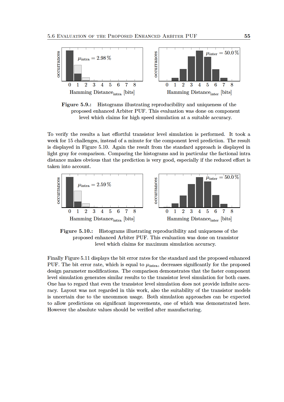
61
Clocking. Figure by MIT OCW. 6.884 - Spring 2005 2/18/05 L06 Clocks 1
 ing Figure by MIT OCW. 6.884 - Spring 2005 2/18/05 L06 s 1 Why s and Storage Elements? Inputs Combinational Logic Outputs Want to reuse combinational logic from cycle to cycle 6.884 - Spring 2005 2/18/05
Flip-Flops, Registers, Counters, and a Simple Processor
 June 8, 22 5:56 vra235_ch7 Sheet number Page number 349 black chapter 7 Flip-Flops, Registers, Counters, and a Simple Processor 7. Ng f3, h7 h6 349 June 8, 22 5:56 vra235_ch7 Sheet number 2 Page number
CMOS, the Ideal Logic Family
 CMOS, the Ideal Logic Family INTRODUCTION Let s talk about the characteristics of an ideal logic family. It should dissipate no power, have zero propagation delay, controlled rise and fall times, and have
EE 42/100 Lecture 24: Latches and Flip Flops. Rev B 4/21/2010 (2:04 PM) Prof. Ali M. Niknejad
 Prof. Ali M. Niknejad") A. M. Niknejad University of California, Berkeley EE 100 / 42 Lecture 24 p. 1/20 EE 42/100 Lecture 24: Latches and Flip Flops ELECTRONICS Rev B 4/21/2010 (2:04 PM) Prof. Ali M. Niknejad University of California,
A. M. Niknejad University of California, Berkeley EE 100 / 42 Lecture 24 p. 1/20 EE 42/100 Lecture 24: Latches and Flip Flops ELECTRONICS Rev B 4/21/2010 (2:04 PM) Prof. Ali M. Niknejad University of California,
Static-Noise-Margin Analysis of Conventional 6T SRAM Cell at 45nm Technology
 Static-Noise-Margin Analysis of Conventional 6T SRAM Cell at 45nm Technology Nahid Rahman Department of electronics and communication FET-MITS (Deemed university), Lakshmangarh, India B. P. Singh Department
Chapter 9 Latches, Flip-Flops, and Timers
 ETEC 23 Programmable Logic Devices Chapter 9 Latches, Flip-Flops, and Timers Shawnee State University Department of Industrial and Engineering Technologies Copyright 27 by Janna B. Gallaher Latches A temporary
Theory of Logic Circuits. Laboratory manual. Exercise 3
 Zakład Mikroinformatyki i Teorii Automatów yfrowych Theory of Logic ircuits Laboratory manual Exercise 3 Bistable devices 2008 Krzysztof yran, Piotr zekalski (edt.) 1. lassification of bistable devices
Lecture 11: Sequential Circuit Design
 Lecture 11: Sequential Circuit esign Outline Sequencing Sequencing Element esign Max and Min-elay Clock Skew Time Borrowing Two-Phase Clocking 2 Sequencing Combinational logic output depends on current
CS311 Lecture: Sequential Circuits
 CS311 Lecture: Sequential Circuits Last revised 8/15/2007 Objectives: 1. To introduce asynchronous and synchronous flip-flops (latches and pulsetriggered, plus asynchronous preset/clear) 2. To introduce
Fundamentals of Microelectronics
 Fundamentals of Microelectronics CH1 Why Microelectronics? CH2 Basic Physics of Semiconductors CH3 Diode Circuits CH4 Physics of Bipolar Transistors CH5 Bipolar Amplifiers CH6 Physics of MOS Transistors
COMBINATIONAL and SEQUENTIAL LOGIC CIRCUITS Hardware implementation and software design
 PH-315 COMINATIONAL and SEUENTIAL LOGIC CIRCUITS Hardware implementation and software design A La Rosa I PURPOSE: To familiarize with combinational and sequential logic circuits Combinational circuits
Fault Modeling. Why model faults? Some real defects in VLSI and PCB Common fault models Stuck-at faults. Transistor faults Summary
 Fault Modeling Why model faults? Some real defects in VLSI and PCB Common fault models Stuck-at faults Single stuck-at faults Fault equivalence Fault dominance and checkpoint theorem Classes of stuck-at
Having read this workbook you should be able to: recognise the arrangement of NAND gates used to form an S-R flip-flop.
 Objectives Having read this workbook you should be able to: recognise the arrangement of NAND gates used to form an S-R flip-flop. describe how such a flip-flop can be SET and RESET. describe the disadvantage
7. Latches and Flip-Flops
 Chapter 7 Latches and Flip-Flops Page 1 of 18 7. Latches and Flip-Flops Latches and flip-flops are the basic elements for storing information. One latch or flip-flop can store one bit of information. The
DM9368 7-Segment Decoder/Driver/Latch with Constant Current Source Outputs
 DM9368 7-Segment Decoder/Driver/Latch with Constant Current Source Outputs General Description The DM9368 is a 7-segment decoder driver incorporating input latches and constant current output circuits
TRUE SINGLE PHASE CLOCKING BASED FLIP-FLOP DESIGN
 TRUE SINGLE PHASE CLOCKING BASED FLIP-FLOP DESIGN USING DIFFERENT FOUNDRIES Priyanka Sharma 1 and Rajesh Mehra 2 1 ME student, Department of E.C.E, NITTTR, Chandigarh, India 2 Associate Professor, Department
Topics of Chapter 5 Sequential Machines. Memory elements. Memory element terminology. Clock terminology
 Topics of Chapter 5 Sequential Machines Memory elements Memory elements. Basics of sequential machines. Clocking issues. Two-phase clocking. Testing of combinational (Chapter 4) and sequential (Chapter
Sequential 4-bit Adder Design Report
 UNIVERSITY OF WATERLOO Faculty of Engineering E&CE 438: Digital Integrated Circuits Sequential 4-bit Adder Design Report Prepared by: Ian Hung (ixxxxxx), 99XXXXXX Annette Lo (axxxxxx), 99XXXXXX Pamela
LAB 7 MOSFET CHARACTERISTICS AND APPLICATIONS
 LAB 7 MOSFET CHARACTERISTICS AND APPLICATIONS Objective In this experiment you will study the i-v characteristics of an MOS transistor. You will use the MOSFET as a variable resistor and as a switch. BACKGROUND
TIMING-DRIVEN PHYSICAL DESIGN FOR DIGITAL SYNCHRONOUS VLSI CIRCUITS USING RESONANT CLOCKING
 TIMING-DRIVEN PHYSICAL DESIGN FOR DIGITAL SYNCHRONOUS VLSI CIRCUITS USING RESONANT CLOCKING BARIS TASKIN, JOHN WOOD, IVAN S. KOURTEV February 28, 2005 Research Objective Objective: Electronic design automation
EE552. Advanced Logic Design and Switching Theory. Metastability. Ashirwad Bahukhandi. (Ashirwad Bahukhandi) bahukhan@usc.edu
 bahukhan@usc.edu") EE552 Advanced Logic Design and Switching Theory Metastability by Ashirwad Bahukhandi (Ashirwad Bahukhandi) bahukhan@usc.edu This is an overview of what metastability is, ways of interpreting it, the issues
EE552 Advanced Logic Design and Switching Theory Metastability by Ashirwad Bahukhandi (Ashirwad Bahukhandi) bahukhan@usc.edu This is an overview of what metastability is, ways of interpreting it, the issues
So far we have investigated combinational logic for which the output of the logic devices/circuits depends only on the present state of the inputs.
 equential Logic o far we have investigated combinational logic for which the output of the logic devices/circuits depends only on the present state of the inputs. In sequential logic the output of the
Chapter 10 Advanced CMOS Circuits
 Transmission Gates Chapter 10 Advanced CMOS Circuits NMOS Transmission Gate The active pull-up inverter circuit leads one to thinking about alternate uses of NMOS devices. Consider the circuit shown in
APPLICATION OF ADVANCED SEARCH- METHODS FOR AUTOMOTIVE DATA-BUS SYSTEM SIGNAL INTEGRITY OPTIMIZATION
 APPLICATION OF ADVANCED SEARCH- METHODS FOR AUTOMOTIVE DATA-BUS SYSTEM SIGNAL INTEGRITY OPTIMIZATION Harald Günther 1, Stephan Frei 1, Thomas Wenzel, Wolfgang Mickisch 1 Technische Universität Dortmund,
路 論 Chapter 15 System-Level Physical Design
 Introduction to VLSI Circuits and Systems 路 論 Chapter 15 System-Level Physical Design Dept. of Electronic Engineering National Chin-Yi University of Technology Fall 2007 Outline Clocked Flip-flops CMOS
TSL213 64 1 INTEGRATED OPTO SENSOR
 TSL 64 INTEGRATED OPTO SENSOR SOES009A D4059, NOVEMBER 99 REVISED AUGUST 99 Contains 64-Bit Static Shift Register Contains Analog Buffer With Sample and Hold for Analog Output Over Full Clock Period Single-Supply
Sequential Logic Design Principles.Latches and Flip-Flops
 Sequential Logic Design Principles.Latches and Flip-Flops Doru Todinca Department of Computers Politehnica University of Timisoara Outline Introduction Bistable Elements Latches and Flip-Flops S-R Latch
Here we introduced (1) basic circuit for logic and (2)recent nano-devices, and presented (3) some practical issues on nano-devices.
 basic circuit for logic and (2)recent nano-devices, and presented (3) some practical issues on nano-devices.") Outline Here we introduced () basic circuit for logic and (2)recent nano-devices, and presented (3) some practical issues on nano-devices. Circuit Logic Gate A logic gate is an elemantary building block
Outline Here we introduced () basic circuit for logic and (2)recent nano-devices, and presented (3) some practical issues on nano-devices. Circuit Logic Gate A logic gate is an elemantary building block
DIGITAL TECHNICS II. Dr. Bálint Pődör. Óbuda University, Microelectronics and Technology Institute
 DIGITAL TECHNICS II Dr. Bálint Pődör Óbuda University, Microelectronics and Technology Institute 2. LECTURE: ELEMENTARY SEUENTIAL CIRCUITS: FLIP-FLOPS 1st year BSc course 2nd (Spring) term 2012/2013 1
UNIVERSITY OF CALIFORNIA College of Engineering Department of Electrical Engineering and Computer Sciences
 UNIVERSITY OF CALIFORNIA College of Engineering Department of Electrical Engineering and Computer Sciences Jan M. Rabaey Homework #1: Circuit Simulation EECS 141 Due Friday, January 30, 5pm, box in 240
ISSCC 2003 / SESSION 13 / 40Gb/s COMMUNICATION ICS / PAPER 13.7
 ISSCC 2003 / SESSION 13 / 40Gb/s COMMUNICATION ICS / PAPER 13.7 13.7 A 40Gb/s Clock and Data Recovery Circuit in 0.18µm CMOS Technology Jri Lee, Behzad Razavi University of California, Los Angeles, CA
CHAPTER 16 MEMORY CIRCUITS
 CHPTER 6 MEMORY CIRCUITS Chapter Outline 6. atches and Flip-Flops 6. Semiconductor Memories: Types and rchitectures 6.3 Random-ccess Memory RM Cells 6.4 Sense-mplifier and ddress Decoders 6.5 Read-Only
Latches, the D Flip-Flop & Counter Design. ECE 152A Winter 2012
 Latches, the D Flip-Flop & Counter Design ECE 52A Winter 22 Reading Assignment Brown and Vranesic 7 Flip-Flops, Registers, Counters and a Simple Processor 7. Basic Latch 7.2 Gated SR Latch 7.2. Gated SR
Application Note 58 Crystal Considerations with Dallas Real Time Clocks
 www.dalsemi.com Application Note 58 Crystal Considerations with Dallas Real Time Clocks Dallas Semiconductor offers a variety of real time clocks (RTCs). The majority of these are available either as integrated
Lecture 10: Sequential Circuits
 Introduction to CMOS VLSI esign Lecture 10: Sequential Circuits avid Harris Harvey Mudd College Spring 2004 Outline q Sequencing q Sequencing Element esign q Max and Min-elay q Clock Skew q Time Borrowing
PowerPC Microprocessor Clock Modes
 nc. Freescale Semiconductor AN1269 (Freescale Order Number) 1/96 Application Note PowerPC Microprocessor Clock Modes The PowerPC microprocessors offer customers numerous clocking options. An internal phase-lock
Introduction to CMOS VLSI Design
 Introduction to CMOS VLSI esign Slides adapted from: N. Weste,. Harris, CMOS VLSI esign, Addison-Wesley, 3/e, 24 Introduction Integrated Circuits: many transistors on one chip Very Large Scale Integration
Step Response of RC Circuits
 Step Response of RC Circuits 1. OBJECTIVES...2 2. REFERENCE...2 3. CIRCUITS...2 4. COMPONENTS AND SPECIFICATIONS...3 QUANTITY...3 DESCRIPTION...3 COMMENTS...3 5. DISCUSSION...3 5.1 SOURCE RESISTANCE...3
Memory Systems. Static Random Access Memory (SRAM) Cell
 Cell") Memory Systems This chapter begins the discussion of memory systems from the implementation of a single bit. The architecture of memory chips is then constructed using arrays of bit implementations coupled
Memory Systems This chapter begins the discussion of memory systems from the implementation of a single bit. The architecture of memory chips is then constructed using arrays of bit implementations coupled
Sequential Logic: Clocks, Registers, etc.
 ENEE 245: igital Circuits & Systems Lab Lab 2 : Clocks, Registers, etc. ENEE 245: igital Circuits and Systems Laboratory Lab 2 Objectives The objectives of this laboratory are the following: To design
DIGITAL-TO-ANALOGUE AND ANALOGUE-TO-DIGITAL CONVERSION
 DIGITAL-TO-ANALOGUE AND ANALOGUE-TO-DIGITAL CONVERSION Introduction The outputs from sensors and communications receivers are analogue signals that have continuously varying amplitudes. In many systems
CHAPTER 3 Boolean Algebra and Digital Logic
 CHAPTER 3 Boolean Algebra and Digital Logic 3.1 Introduction 121 3.2 Boolean Algebra 122 3.2.1 Boolean Expressions 123 3.2.2 Boolean Identities 124 3.2.3 Simplification of Boolean Expressions 126 3.2.4
Supply voltage Supervisor TL77xx Series. Author: Eilhard Haseloff
 Supply voltage Supervisor TL77xx Series Author: Eilhard Haseloff Literature Number: SLVAE04 March 1997 i IMPORTANT NOTICE Texas Instruments (TI) reserves the right to make changes to its products or to
Use and Application of Output Limiting Amplifiers (HFA1115, HFA1130, HFA1135)
") Use and Application of Output Limiting Amplifiers (HFA111, HFA110, HFA11) Application Note November 1996 AN96 Introduction Amplifiers with internal voltage clamps, also known as limiting amplifiers, have
Use and Application of Output Limiting Amplifiers (HFA111, HFA110, HFA11) Application Note November 1996 AN96 Introduction Amplifiers with internal voltage clamps, also known as limiting amplifiers, have
Chapter 19 Operational Amplifiers
 Chapter 19 Operational Amplifiers The operational amplifier, or op-amp, is a basic building block of modern electronics. Op-amps date back to the early days of vacuum tubes, but they only became common
CO2005: Electronics I (FET) Electronics I, Neamen 3th Ed. 1
 Electronics I, Neamen 3th Ed. 1") CO2005: Electronics I The Field-Effect Transistor (FET) Electronics I, Neamen 3th Ed. 1 MOSFET The metal-oxide-semiconductor field-effect transistor (MOSFET) becomes a practical reality in the 1970s. The
CO2005: Electronics I The Field-Effect Transistor (FET) Electronics I, Neamen 3th Ed. 1 MOSFET The metal-oxide-semiconductor field-effect transistor (MOSFET) becomes a practical reality in the 1970s. The
S-Band Low Noise Amplifier Using the ATF-10136. Application Note G004
 S-Band Low Noise Amplifier Using the ATF-10136 Application Note G004 Introduction This application note documents the results of using the ATF-10136 in low noise amplifier applications at S band. The ATF-10136
StarRC Custom: Next-Generation Modeling and Extraction Solution for Custom IC Designs
 White Paper StarRC Custom: Next-Generation Modeling and Extraction Solution for Custom IC Designs May 2010 Krishnakumar Sundaresan Principal Engineer and CAE Manager, Synopsys Inc Executive Summary IC
Experiment # 9. Clock generator circuits & Counters. Eng. Waleed Y. Mousa
 Experiment # 9 Clock generator circuits & Counters Eng. Waleed Y. Mousa 1. Objectives: 1. Understanding the principles and construction of Clock generator. 2. To be familiar with clock pulse generation
Making Accurate Voltage Noise and Current Noise Measurements on Operational Amplifiers Down to 0.1Hz
 Author: Don LaFontaine Making Accurate Voltage Noise and Current Noise Measurements on Operational Amplifiers Down to 0.1Hz Abstract Making accurate voltage and current noise measurements on op amps in
TDA4605 CONTROL CIRCUIT FOR SWITCH MODE POWER SUPPLIES USING MOS TRANSISTORS
 CONTROL CIRCUIT FOR SWITCH MODE POWER SUPPLIES USING MOS TRANSISTORS Fold-Back Characteristic provides Overload Protection for External Diodes Burst Operation under Short-Circuit and no Load Conditions
Latch Timing Parameters. Flip-flop Timing Parameters. Typical Clock System. Clocking Overhead
 Clock - key to synchronous systems Topic 7 Clocking Strategies in VLSI Systems Peter Cheung Department of Electrical & Electronic Engineering Imperial College London Clocks help the design of FSM where
ARRL Morse Code Oscillator, How It Works By: Mark Spencer, WA8SME
 The national association for AMATEUR RADIO ARRL Morse Code Oscillator, How It Works By: Mark Spencer, WA8SME This supplement is intended for use with the ARRL Morse Code Oscillator kit, sold separately.
Computer Networks and Internets, 5e Chapter 6 Information Sources and Signals. Introduction
 Computer Networks and Internets, 5e Chapter 6 Information Sources and Signals Modified from the lecture slides of Lami Kaya (LKaya@ieee.org) for use CECS 474, Fall 2008. 2009 Pearson Education Inc., Upper
Lecture 7: Clocking of VLSI Systems
 Lecture 7: Clocking of VLSI Systems MAH, AEN EE271 Lecture 7 1 Overview Reading Wolf 5.3 Two-Phase Clocking (good description) W&E 5.5.1, 5.5.2, 5.5.3, 5.5.4, 5.5.9, 5.5.10 - Clocking Note: The analysis
PROGETTO DI SISTEMI ELETTRONICI DIGITALI. Digital Systems Design. Digital Circuits Advanced Topics
 PROGETTO DI SISTEMI ELETTRONICI DIGITALI Digital Systems Design Digital Circuits Advanced Topics 1 Sequential circuit and metastability 2 Sequential circuit - FSM A Sequential circuit contains: Storage
NAME AND SURNAME. TIME: 1 hour 30 minutes 1/6
 E.T.S.E.T.B. MSc in ICT FINAL EXAM VLSI Digital Design Spring Course 2005-2006 June 6, 2006 Score publication date: June 19, 2006 Exam review request deadline: June 22, 2006 Academic consultancy: June
International Journal of Electronics and Computer Science Engineering 1482
 International Journal of Electronics and Computer Science Engineering 1482 Available Online at www.ijecse.org ISSN- 2277-1956 Behavioral Analysis of Different ALU Architectures G.V.V.S.R.Krishna Assistant
Evaluating AC Current Sensor Options for Power Delivery Systems
 Evaluating AC Current Sensor Options for Power Delivery Systems State-of-the-art isolated ac current sensors based on CMOS technology can increase efficiency, performance and reliability compared to legacy
Introduction to CMOS VLSI Design (E158) Lecture 8: Clocking of VLSI Systems
 Lecture 8: Clocking of VLSI Systems") Harris Introduction to CMOS VLSI Design (E158) Lecture 8: Clocking of VLSI Systems David Harris Harvey Mudd College David_Harris@hmc.edu Based on EE271 developed by Mark Horowitz, Stanford University MAH
Harris Introduction to CMOS VLSI Design (E158) Lecture 8: Clocking of VLSI Systems David Harris Harvey Mudd College David_Harris@hmc.edu Based on EE271 developed by Mark Horowitz, Stanford University MAH
NTE2053 Integrated Circuit 8 Bit MPU Compatible A/D Converter
 NTE2053 Integrated Circuit 8 Bit MPU Compatible A/D Converter Description: The NTE2053 is a CMOS 8 bit successive approximation Analog to Digital converter in a 20 Lead DIP type package which uses a differential
Quad 2-input NAND Schmitt trigger
 Rev. 9 15 December 2015 Product data sheet 1. General description 2. Features and benefits 3. Applications The is a quad two-input NAND gate. Each input has a Schmitt trigger circuit. The gate switches
Introduction to VLSI Programming. TU/e course 2IN30. Prof.dr.ir. Kees van Berkel Dr. Johan Lukkien [Dr.ir. Ad Peeters, Philips Nat.
 Introduction to VLSI Programming TU/e course 2IN30 Prof.dr.ir. Kees van Berkel Dr. Johan Lukkien [Dr.ir. Ad Peeters, Philips Nat.Lab] Introduction to VLSI Programming Goals Create silicon (CMOS) awareness
1ED Compact A new high performance, cost efficient, high voltage gate driver IC family
 1ED Compact A new high performance, cost efficient, high voltage gate driver IC family Heiko Rettinger, Infineon Technologies AG, Am Campeon 1-12, 85579 Neubiberg, Germany, heiko.rettinger@infineon.com
Small Signal Analysis of a PMOS transistor Consider the following PMOS transistor to be in saturation. Then, 1 2
 Small Signal Analysis of a PMOS transistor Consider the following PMOS transistor to be in saturation. Then, 1 I SD = µ pcox( VSG Vtp)^2(1 + VSDλ) 2 From this equation it is evident that I SD is a function
Understanding Power Impedance Supply for Optimum Decoupling
 Introduction Noise in power supplies is not only caused by the power supply itself, but also the load s interaction with the power supply (i.e. dynamic loads, switching, etc.). To lower load induced noise,
Timing Methodologies (cont d) Registers. Typical timing specifications. Synchronous System Model. Short Paths. System Clock Frequency
 Registers. Typical timing specifications. Synchronous System Model. Short Paths. System Clock Frequency") Registers Timing Methodologies (cont d) Sample data using clock Hold data between clock cycles Computation (and delay) occurs between registers efinition of terms setup time: minimum time before the clocking
Registers Timing Methodologies (cont d) Sample data using clock Hold data between clock cycles Computation (and delay) occurs between registers efinition of terms setup time: minimum time before the clocking
Alpha CPU and Clock Design Evolution
 Alpha CPU and Clock Design Evolution This lecture uses two papers that discuss the evolution of the Alpha CPU and clocking strategy over three CPU generations Gronowski, Paul E., et.al., High Performance
Module 2. Embedded Processors and Memory. Version 2 EE IIT, Kharagpur 1
 Module 2 Embedded Processors and Memory Version 2 EE IIT, Kharagpur 1 Lesson 5 Memory-I Version 2 EE IIT, Kharagpur 2 Instructional Objectives After going through this lesson the student would Pre-Requisite
Analyzing Electrical Effects of RTA-driven Local Anneal Temperature Variation
 1 Analyzing Electrical Effects of RTA-driven Local Anneal Temperature Variation Vivek Joshi, Kanak Agarwal*, Dennis Sylvester, David Blaauw Electrical Engineering & Computer Science University of Michigan,
Computer Network. Interconnected collection of autonomous computers that are able to exchange information
 Introduction Computer Network. Interconnected collection of autonomous computers that are able to exchange information No master/slave relationship between the computers in the network Data Communications.
Network Security. Chapter 6 Random Number Generation
 Network Security Chapter 6 Random Number Generation 1 Tasks of Key Management (1)! Generation:! It is crucial to security, that keys are generated with a truly random or at least a pseudo-random generation
1. True or False? A voltage level in the range 0 to 2 volts is interpreted as a binary 1.
 File: chap04, Chapter 04 1. True or False? A voltage level in the range 0 to 2 volts is interpreted as a binary 1. 2. True or False? A gate is a device that accepts a single input signal and produces one
Agenda. Michele Taliercio, Il circuito Integrato, Novembre 2001
 Agenda Introduzione Il mercato Dal circuito integrato al System on a Chip (SoC) La progettazione di un SoC La tecnologia Una fabbrica di circuiti integrati 28 How to handle complexity G The engineering
Op-Amp Simulation EE/CS 5720/6720. Read Chapter 5 in Johns & Martin before you begin this assignment.
 Op-Amp Simulation EE/CS 5720/6720 Read Chapter 5 in Johns & Martin before you begin this assignment. This assignment will take you through the simulation and basic characterization of a simple operational
DDX 7000 & 8003. Digital Partial Discharge Detectors FEATURES APPLICATIONS
 DDX 7000 & 8003 Digital Partial Discharge Detectors The HAEFELY HIPOTRONICS DDX Digital Partial Discharge Detector offers the high accuracy and flexibility of digital technology, plus the real-time display
Sequential Circuit Design
 Sequential Circuit Design Lan-Da Van ( 倫 ), Ph. D. Department of Computer Science National Chiao Tung University Taiwan, R.O.C. Fall, 2009 ldvan@cs.nctu.edu.tw http://www.cs.nctu.edu.tw/~ldvan/ Outlines
SECTION 2 Transmission Line Theory
 SEMICONDUCTOR DESIGN GUIDE Transmission Line Theory SECTION 2 Transmission Line Theory Introduction The ECLinPS family has pushed the world of ECL into the realm of picoseconds. When output transitions
Lecture 24. Inductance and Switching Power Supplies (how your solar charger voltage converter works)
") Lecture 24 Inductance and Switching Power Supplies (how your solar charger voltage converter works) Copyright 2014 by Mark Horowitz 1 Roadmap: How Does This Work? 2 Processor Board 3 More Detailed Roadmap
Lecture 24 Inductance and Switching Power Supplies (how your solar charger voltage converter works) Copyright 2014 by Mark Horowitz 1 Roadmap: How Does This Work? 2 Processor Board 3 More Detailed Roadmap
S. Venkatesh, Mrs. T. Gowri, Department of ECE, GIT, GITAM University, Vishakhapatnam, India
 Power reduction on clock-tree using Energy recovery and clock gating technique S. Venkatesh, Mrs. T. Gowri, Department of ECE, GIT, GITAM University, Vishakhapatnam, India Abstract Power consumption of
Digital to Analog Converter. Raghu Tumati
 Digital to Analog Converter Raghu Tumati May 11, 2006 Contents 1) Introduction............................... 3 2) DAC types................................... 4 3) DAC Presented.............................
Synchronization of sampling in distributed signal processing systems
 Synchronization of sampling in distributed signal processing systems Károly Molnár, László Sujbert, Gábor Péceli Department of Measurement and Information Systems, Budapest University of Technology and
PUF Physical Unclonable Functions
 Physical Unclonable Functions Protecting next-generation Smart Card ICs with SRAM-based s The use of Smart Card ICs has become more widespread, having expanded from historical banking and telecommunication
Gates. J. Robert Jump Department of Electrical And Computer Engineering Rice University Houston, TX 77251
 Gates J. Robert Jump Department of Electrical And Computer Engineering Rice University Houston, T 77251 1. The Evolution of Electronic Digital Devices...1 2. Logical Operations and the Behavior of Gates...2
Content Map For Career & Technology
 Content Strand: Applied Academics CT-ET1-1 analysis of electronic A. Fractions and decimals B. Powers of 10 and engineering notation C. Formula based problem solutions D. Powers and roots E. Linear equations
Sequential Circuits. Combinational Circuits Outputs depend on the current inputs
 Principles of VLSI esign Sequential Circuits Sequential Circuits Combinational Circuits Outputs depend on the current inputs Sequential Circuits Outputs depend on current and previous inputs Requires separating
Reconfigurable ECO Cells for Timing Closure and IR Drop Minimization. TingTing Hwang Tsing Hua University, Hsin-Chu
 Reconfigurable ECO Cells for Timing Closure and IR Drop Minimization TingTing Hwang Tsing Hua University, Hsin-Chu 1 Outline Introduction Engineering Change Order (ECO) Voltage drop (IR-DROP) New design
Lesson 12 Sequential Circuits: Flip-Flops
 Lesson 12 Sequential Circuits: Flip-Flops 1. Overview of a Synchronous Sequential Circuit We saw from last lesson that the level sensitive latches could cause instability in a sequential system. This instability
Application Note AN-1068 reva
 Application Note AN-1068 reva Considerations for Designs Using Radiation-Hardened Solid State Relays By Alan Tasker Table of Contents Introduction Page Overview...1 The Contact...1 Actuation...1 The IR
School of Engineering Department of Electrical and Computer Engineering
 1 School of Engineering Department of Electrical and Computer Engineering 332:223 Principles of Electrical Engineering I Laboratory Experiment #4 Title: Operational Amplifiers 1 Introduction Objectives
www.jameco.com 1-800-831-4242
 Distributed by: www.jameco.com 1-800-831-4242 The content and copyrights of the attached material are the property of its owner. LF411 Low Offset, Low Drift JFET Input Operational Amplifier General Description
Digital Electronics Detailed Outline
 Digital Electronics Detailed Outline Unit 1: Fundamentals of Analog and Digital Electronics (32 Total Days) Lesson 1.1: Foundations and the Board Game Counter (9 days) 1. Safety is an important concept
Yaffs NAND Flash Failure Mitigation
 Yaffs NAND Flash Failure Mitigation Charles Manning 2012-03-07 NAND flash is one of very few types of electronic device which are knowingly shipped with errors and are expected to generate further errors
PACKAGE OUTLINE DALLAS DS2434 DS2434 GND. PR 35 PACKAGE See Mech. Drawings Section
 PRELIMINARY DS2434 Battery Identification Chip FEATURES Provides unique ID number to battery packs PACKAGE OUTLINE Eliminates thermistors by sensing battery temperature on chip DALLAS DS2434 1 2 3 256
14-stage ripple-carry binary counter/divider and oscillator
 Rev. 8 25 March 2016 Product data sheet 1. General description 2. Features and benefits 3. Ordering information The is a with three oscillator terminals (RS, REXT and CEXT), ten buffered outputs (Q3 to
Reading: HH Sections 4.11 4.13, 4.19 4.20 (pgs. 189-212, 222 224)
") 6 OP AMPS II 6 Op Amps II In the previous lab, you explored several applications of op amps. In this exercise, you will look at some of their limitations. You will also examine the op amp integrator and
6 OP AMPS II 6 Op Amps II In the previous lab, you explored several applications of op amps. In this exercise, you will look at some of their limitations. You will also examine the op amp integrator and
Chapter 6: From Digital-to-Analog and Back Again
 Chapter 6: From Digital-to-Analog and Back Again Overview Often the information you want to capture in an experiment originates in the laboratory as an analog voltage or a current. Sometimes you want to
MAS.836 HOW TO BIAS AN OP-AMP
 MAS.836 HOW TO BIAS AN OP-AMP Op-Amp Circuits: Bias, in an electronic circuit, describes the steady state operating characteristics with no signal being applied. In an op-amp circuit, the operating characteristic
ECE124 Digital Circuits and Systems Page 1
 ECE124 Digital Circuits and Systems Page 1 Chip level timing Have discussed some issues related to timing analysis. Talked briefly about longest combinational path for a combinational circuit. Talked briefly