Solar Cell Technology State of the Art
|
|
|
- Edward Eaton
- 8 years ago
- Views:
Transcription
1 Solar Cell Technology State of the Art Summer School - Energia per il domani Sesto Pusteria, June th, 2013 Vanni Lughi DI 3 Dipartimento di Ingegneria e Architettura, University of Trieste, Italy vlughi@units.it

2 Basic Solar Cell Concept Absorber s Requirements: Bandgap matched with solar spectrum ( 1.5 ev) Good transport properties Full absorption within absorber s thickness + -
3 Giunzione p-n
4 Giunzione p-n Energiy p n E p Conduction band Valence band n Spatial coordinate
5 Energy Photovoltaic Effect 1. Absorption of solar radiation Creation of free carriers Free carrier extraction Electrical energy
6 Photovoltaic Effect Selection of Materials 1. Absorption of solar radiation Materials with good absorption of the solar radiation Creation of free carriers 2. Free carrier extraction Electrical energy Perfect materials (large mean free paths for the carriers) Short carrier paths
7 Current Main Technology: Silicon 200 m 3.5 kg Si /kw p
 Equazioni di diffusione Correnti di deriva sono trascurabili Equazioni della densità di")
8 Derivazione della caratteristica IV Condizioni al contorno: ai contatti (ohmica o ricombinazione) e alla giunzione (legge della giunzione) Equazioni di diffusione Correnti di deriva sono trascurabili Equazioni della densità di corrente

9 Caratteristica IV e circuito equivalente
10 Figure di merito Corrente di corto circuito Isc, efficienza quantica QE, risposta spettrale SR Tensione di circuito aperto Voc Rendimento
11 Efficienza della cella solare
12 Limiti termodinamici Limite di Carnot Carnot TA 1 95% T S T A : temperatura della cella pari alla T ambiente T S : temperatura del sole Limite di Landsberg 93.3% (86.8%, assumendo una serie di corpi neri come convertitore) Limite di Schokley Queisser (SQ): il convertitore è un semiconduttore

13 Perdite Ombreggiamento Riflessione Trasmissione Ricombinazione Termalizzazione di fotoni energetici Perdite alla giunzione Resistenze parassite Perdite ai contatti
14 Celle solari reali Rs: Resistenza di serie Rp: Resistenza di shunt (parallela)
15 Effetto della temperatura V OC T 2.3 mv C -1
16 Photovoltaic modules Photovoltaic modules are the fundamental element of the photovoltaic generator Commercial crystalline silicon modules
17
18
19 Cost Stability
20 Why Thin Film Solar Cells? Absorption Coefficient [cm -1 ] Reduce amount of active material by using high absorption coefficient materials Conduction band Direct Bandgap Conduction band Phonon Absorption Valence band Indirect Bandgap Indirect Absorption Direct Absorption Valence band Photon Energy [ev]
21 Advantages of Thin Film Solar Cells Use of less material ( 2 orders of magnitude) Low and stable cost Sustainability of supply Integrated fabrication Wide variety of substrates available Opportunity for integrated device design (e.g. Building Integrated Photovoltaics - BIPV) Flexibility on the material chemistry optimization of bandgap Short travel distances for the carriers enhanced collection Flexible device design (bandgap engineering)
22 Fraction of Useful Photons Absorbed Designing Film Thickness Lambert Beer I = I0 exp (- z) I0 f ( d) 0 (1 exp( ( ) d) N g 0 N ph ( ) d ph ( ) d z Thickness [ m]
23 Cost Stability The active material counts for about 5 10% of the overall cost (in Si technology, it is about 50%) COSTO DELLE MATERIE PRIME Modulo fotovoltaico Distinta Materie prime Costo per pezzo Vetro1 43,20 Antiriflesso 0,30 ITO 3,30 CdS 0,03 CdTe 2,50 CdCl2 0,30 Cu 0,01 EVA 1,04 Vetro2 10,80 Collegamento 1,35 Contatto oro 3,00 ZnTe 0,50 Tot 66,33 Costo Imballaggi Cartoni 0,50 Tot 0,50 Costo Totale Prodotto 1 66,83

24 Cost Learning Curve
25 Advantages of Thin Film Solar Cells Use of less material ( 2 orders of magnitude) Low and stable cost Sustainability of supply Integrated fabrication Wide variety of substrates available Opportunity for integrated device design (e.g. Building Integrated Photovoltaics - BIPV) Flexibility on the material chemistry optimization of bandgap Short travel distances for the carriers enhanced collection Flexible device design (bandgap engineering)
26 PV modules thin film technology - Structure and fabrication - Continuous process Sequential deposition of thin films on glass (superstrate structure) or on the back electrode (substrate structure) The output is an integrated module, where the cells in series are formed a posteriori via laser cutting

27 + - Basic Solar Cell Design
28 Thin Film Solar Cell (superstrate) 200 nm 50 nm 5000 nm 200 nm 200 nm
 50 nm 5000 nm 200")
29 200 nm Thin Film Solar Cell (substrate) 50 nm 5000 nm 200 nm
30 Photovoltaic modules Colored modules ( mimetic ) Semi-transparent modules Flexible modules
31 Building Integration
32 Advantages of Thin Film Solar Cells Use of less material ( 2 orders of magnitude) Low and stable cost Sustainability of supply Integrated fabrication Wide variety of substrates available Opportunity for integrated device design (e.g. Building Integrated Photovoltaics - BIPV) Flexibility on the material chemistry optimization of bandgap Short travel distances for the carriers enhanced collection Flexible device design (bandgap engineering)
33 a-si:h (amorphous silicon) nm Direct bandgap: 1.7 ev (tunable with Ge alloying) Convenient large scale deposition methods (mainly CVD and PE-CVD at C) X Need to stabilize performance (Staebler-Wronsky) Key design issue: i-layer quality and thickness (tradeoff btw absorption and collection) Need to minimize absorption within the p-level (e.g. alloying with carbon -> window layer (2eV) nm glass TCO p-sic:h i-si:h n-si:h ZnO Ag/Al

34 Tandem cell Thin Film Silicon - variants c-si:h Bandgap 1.1 ev No degradation poly-si Bandgap 1.1 ev No degradation Good conduction

35 CdTe Thin Film Solar Cells Perfection requirements of materials are relaxed
36 Cadmium Telluride Thin Film Solar Cells Ideal bandgap High absorption coefficient Fast e-h separation (e.b.e. 10 mev) High mobility: 1000 cm 2 /V s - electrons 80 cm 2 /V s - holes Band bending at grain boundary -> reduced recombination Current limitations: Contacts and surface recomb. Variety of deposition processes (sputtering, CSS, electrochemical, evaporation) Key to process: activation treatment at 500 C (crystal quality improves, intermixing at CdS/CdTe interface, p-doping established, defects annealed, )


37 DMRN: Ricerca su celle a film sottile di CdTe Tipica sezione trasversale Modulo fotovoltaico al CdTe Cella al CdTe su substrato flessibile


38 counts DMRN: Ricerca su celle a film sottile di CdTe 30W PET (220) (311)?? θ

39 CIGS Thin Film Solar Cells Tunable bandgap Deposition by co-evaporation (!) Many aspects similar to CdTe datasheet
40 A new player: CZTS (Copper Zinc Tin Sulfide) Bandgap 1.4 High absorption coefficient ( > 10 4 in the visible range) Abundant, environmentally friendly elements Many aspects similar to CIGS and CdTe Variety of deposition methods available (nanoinks, electrochemistry, sputtering, EB-PVD, PLD, sol gel.)
41 Energy PV efficiency: Thermodynamic limit Conduction Band Valence Band Max efficiency: 30%
42 Beyond The Single Junction Limit: Tandem cells More efficient use of the solar spectrum
43 Tandem Cells Thermodynamic limiting efficiency: 86.8% Current efficiency record > 40% Multijunction cells very expensive Aerospace applications or terrestrial concentration
44
45
46
47 Thin Film Solar Cells Medium efficiency Low Cost a-si:h 10.1 Cell Record Module Record a-si:h - tandem CdTe CIGS CZTS 9.7 N/A III-V multijunction 33.8 (41.6) N/A DSSC (s) Organic (s) Techno-economical analysis will follow
48 Thin Film Solar Cells - Production Potential isupply Corp., 2011
49 Thin Film Solar Cells Shipments and Pricing isupply Corp., 2011
50 Thin Film Solar Cells Market Shares isupply Corp., 2011
51 Thin Film Solar Cells Slight slowdown isupply Corp., 2011
52 Disponibilità delle materie prime e sostenibilità degli approvvigionamenti Nota: Il cadmio è un sottoprodotto dell estrazione dello zinco Disponibile principalmente in Cina, Australia ed USA Data from NREL, USA Si tende a non utilizzare più il cadmio nelle nuove tecnologie (es: Pile Ni-Cd) attesa grande disponibilità a basso prezzo La disponibiltà di cadmio non limita la produttività di moduli al CdTe
53 Disponibilità delle materie prime e sostenibilità degli approvvigionamenti Tellurio è l elemento più scarso tra quelli richiesti per produrre moduli al CdTe Gli attuali ritmi di estrazione assicurano una produzione annua di 29 GWp/anno: 5 volte la produzione complessiva annuale di fotovoltaico 100 volte l attuale produzione basata su CdTe L estrazione di tellurio può venir incrementata di 15 volte senza costi aggiuntivi Dati NREL, USA

54 CdTe e l ambiente CdTe è un composto stabile e non rilascia Cd nemmeno in condizioni estreme I quantitativi di Cd nei moduli sono minimi Anche altre tecnologie fotovoltaiche contengono Cd I moduli al CdTe rappresentano un modo per fissare il Cd I moduli al CdTe sono quasi interamente riciclabili Separazione dell hardware strutturale ed elettrico dal modulo Comminuzione e separazione tra vetro e solidi contenenti cadmio Riciclaggio del vetro Estrazione e raffinazione dei metalli
55 CdTe e l ambiente Table 1. Sources and Relative Contributions of Cd Exposure to Humans (in Europe) Phosphate fertilizers 41.3 % Fossil fuel combustion 22.0 % Iron and steel 16.7 % production Natural sources 8.0 % Non-ferrous metals 6.3 % Cement production 2.5 % Cadmium products 2.5 % Incineration 1.0 % When PV replaces burning coal for electricity generation, it will prevent a minimum of 2 g of Cd in gaseous emissions and about 140 g of Cd in ash form for each GWh of electricity produced

56 Riuso del CdTe
57 Thin Films - Concluding Remarks There is a number of commercially available thin film technologies - excellent alternatives to silicon in some applications (e.g. for area-based design of installations) The thin film PV market is potentially vast and untapped There is a variety of potentially viable new technologies (e.g. CZTS)
58 Photovoltaic modules Concentration: Requires tracking systems In principle efficiency is higher
59 Efficeincy Technology evolution: Efficiency increase 24.7% 30% (theoretical limit) Silicon CdTe Thin film 16.5% 2009 Time
60 Efficiency (%) Tecno-Economical Evolution - Cost and Efficiency PV Figures of Merit $/W 0.2 $/W Grid parity 0.5 $/W Economical convenience Ultimate thermodynamic limit 40 1 $/W SQ limit for single junction 20 Thin film technology Silicon technology 3.5 $/W Cost ($/m 2 )
61 Thin Film Solar Cells Young Technology (max efficiency is 30-40% of thermodynamic limit) Films can be deposited on various substrates (flexible, architectural elements for building integration, etc.) Low Cost Thermodynamic limit is still 30%
62 Efficiency (%) Tecno-Economical Evolution - Cost and Efficiency PV Figures of Merit $/W 0.2 $/W Grid parity 0.5 $/W Economical convenience Ultimate thermodynamic limit 40 1 $/W Multijunctions SQ limit for single junction 20 Thin film technology Silicon technology 3.5 $/W Cost ($/m 2 )
63 Dye-sensitized solar cell (DSSC) Grätzel cell - Decreasing cost -
 Grätzel")

64 Dye-sensitized solar cell (DSSC) Grätzel cell Efficiency ~ 5-10% Liquid electrolyte DSSC c-si

65 Photosynthesis - mastering charge separation - Energy is absorbed by the antenna complexes Cascade of energy transfer between donors and acceptors embedded in antennas (FRET) Energy is funneled to the reaction center Subsequent multistep electron transfer This creates a charge-separated state which lasts for 10s of s or more, with a ~100% QE Limitations Absorption is only efficient at specific wavelenghts To reach the charge-separated state the electron needs to spend energy Energy converted in chemical energy ~ 9%
 Quantum yield: 0.5% Lifetime 0.")
66 Artificial Photosynthesis: Basic Example Porphyrin-fullerene couples self-assembled on surfaces Donors and acceptors are bonded covalently Thiol Porphyrin C 60 Methil Viologen (MV 2+ ) Quantum yield: 0.5% Lifetime 0.77 s Loose packaging on the surface
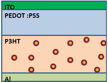
67 Artificial Photosynthesis Requirements Appropriate redox potentials and excitation energy for donors and acceptors (quantum yield) Small reorganization energy (- G cs ~ and - G CR >> ) to favor forward electron transfer (charge separation time) Distance between donors and acceptors Solvent characteristics Vibrational modes of the molecules

68 Artificial Photosynthesis: A more efficient scheme Ferrocene Porphyrin C 60 Quantum yield > 25% Lifetime ~ 16 s Dense packaging on the surface Pentads do even better H. Imahori et al., Adv. Func. Materials 14, 525 (2004)

69 Artificial Photosynthesis: Mimicking energy transfer Boron Dipyrrin Thiol Ferrocene Porphyrin Quantum yield: up to 50% Enhanced spectral absorption Dense packaging on the surface H. Imahori et al., Adv. Func. Materials 14, 525 (2004)
70 Artificial Photosynthesis on Transparent Conductive Oxide (ITO) Avoids quenching by electrode Transparent substrate H. Imahori et al., Adv. Func. Materials 14, 525 (2004)

71 Artificial Photosynthesis: Hierarchical assembly for enhancing absorption C 60 Porphirine H. Imahori et al., Adv. Func. Materials 14, 525 (2004)

72 Artificial Photosynthesis: Hierarchical assembly for enhancing absorption Gold nanoparticle H. Imahori et al., Adv. Func. Materials 14, 525 (2004)


73 Stealing from Nature Photoactive reaction centers on metal substrates e - L. Forlov et al., Adv. Materials 17, 2434 (2005)
74 Celle multigiunzione Superare il dilemma del bandgap Efficienza record > 42% Estremamente complesse e costose
75 Materiali a banda elettronica intermedia Un modo elegante per superare il dilemma del bandgap

76 Making an Intermediate Band Material Quantum dots embedded in a semiconductor Nanotechnology at the service of PV Banda di conduzione Banda di valenza Banda intermedia

77 Photovoltaic Devices Based on Intermediate Band Materials Max efficiency 47% Scalable, low-cost production approaches Diversity of substrates excellent integration (nanoinks and photovoltaic paints)

78 Hybrid Cells Organic + Fullerene-capped Quantum Dots
79 Hybrid Cells Organic + Fullerenecapped Quantum Dots
80 Efficiency (%) Tecno-Economical Evolution - Cost and Efficiency PV Figures of Merit $/W 0.2 $/W Grid parity 0.5 $/W Economical convenience Ultimate thermodynamic limit 40 IB Materials 1 $/W Multijunctions SQ limit for single junction 20 Thin film technology Silicon technology 3.5 $/W Cost ($/m 2 )
81 Efficiency 47% (IB material limit) 24.7% 30% (single junction limit) Silicio 16.5% CdTe 2008 Time
82 Beyond The Single Junction Limit: Other approaches Multiple carrier generation using high energy photons to extract more than one electron per photon (next slide) Hot electron extraction extracting high energy photogenerated electrons before they thermalize Thermodynamic limiting efficiency (both cases): 86.8%
83 Multiple Exciton Generation - MEG Wasted energy! Use highenergy photons