Understanding the p-n Junction by Dr. Alistair Sproul Senior Lecturer in Photovoltaics The Key Centre for Photovoltaic Engineering, UNSW
|
|
|
- Irene Anthony
- 8 years ago
- Views:
Transcription
1 Understanding the p-n Junction by Dr. Alistair Sproul Senior Lecturer in Photovoltaics The Key Centre for Photovoltaic Engineering, UNSW The p-n junction is the fundamental building block of the electronic age. Most electronic devices are made of silicon. By exploring the electrical properties of silicon, it is possible to acquire an understanding of the inner workings of the p-n junction. Silicon A single silicon atom consists of fourteen negatively charged electrons surrounding a nucleus of fourteen positively charged protons and fourteen electrically neutral neutrons. As there are an equal number of positive and negative charges, the silicon atom has no net electric charge. Of the fourteen electrons, only the four outer electrons (visualised as those on the outermost shell of the atom) are available for chemical bonding. The remaining 10 electrons are tightly bound to the nucleus and do not form bonds to other atoms. Dr. Alistair Sproul is a senior lecturer at the Key Centre for Photovoltaic Engineering, UNSW. He specialises in teaching Photovoltaics and Renewable Energy Engineering courses at the undergraduate and postgraduate levels. He is also a consultant to industry where he provides expert advice in the optimisation of renewable energy systems. In a crystal of silicon, each silicon atom bonds to four other silicon atoms. Each bond consists of two electrons, one electron from each of the silicon atoms involved in the bond. This type of bonding, where electrons are shared equally by the atoms involved, is called covalent bonding. These four bonding electrons give silicon a very nice property: it can form a crystal involving all of the bonding electrons, with none left over. (Carbon, which also has four bonding electrons, can use all four of its electrons in covalent carbon-carbon bonds and form crystals of diamond.) A silicon crystal consists of atoms that have no net electric charge (having the same number of electrons as protons) and therefore the silicon crystal itself has no net electric charge. Because of its electrical properties, silicon is called a semiconductor. If the silicon crystal is very pure, then the outer four electrons occupy all of the covalent bonds in the crystal. At temperatures near absolute zero the electrons remain in their bonding positions. In this case, a silicon crystal is nearly a perfect electrical insulator. If, however, sufficient energy is supplied to the crystal, by heat or light, it is possible to break some of these covalent bonds. In silicon, the bonding energy of the covalent bond is 1.1 electron volts. When a bond is supplied with this amount of energy (or more) an electron can break free of an atom and the electron is then free to move throughout the crystal. An energy of 1.1 electron volts corresponds to a photon in the near infrared region of the electromagnetic spectrum. A photon with less than 1.1 electron volts of energy does not have enough energy to interact with a bond in the silicon crystal and will therefore pass right through the crystal without dislodging any electrons. Excerpt from Solar Cells: Resource for the Secondary Science Teacher Available from the UNSW Bookshop 13

2 Phosphorus A single phosphorus atom also has no net electric charge. Phosphorus is the next element up from silicon in the periodic table with fifteen electrons and fifteen protons. Again, the negative electric charges from the electrons exactly counteract the positive electric charges from the protons resulting in an atom that has no net electric charge. Of these fifteen electrons, only five of them (again visualised as those on the outermost shell of the atom) are available for chemical bonding. The configuration of these five available bonding electrons gives phosphorus its distinct chemical properties. For p-n junctions the important aspect is that phosphorus has one more electron available for bonding than silicon. Substituting with Phosphorus In a process called "doping", impurity atoms are placed in very pure silicon to change the electrical characteristics of the crystal. Phosphorus can replace some of the silicon atoms in the crystal and when this happens the phosphorus atom is called a dopant atom. The dopant phosphorus atoms each form four covalent bonds in the same way that a silicon atom does with its neighbours. The fifth of the phosphorus bonding electrons, the one that is not used in covalent bonding, now plays an important role. This electron is only weakly attached to the phosphorus atom: so weakly (0.045 electron volts bonding energy) that at normal temperatures the thermal energy within the crystal is sufficient to free it from the phosphorus atom. When this happens the resulting untethered electron is free to travel around the crystal. An electric field. Diode Transistor The positive point charge. The direction of the electric field. The Direction of the Electric Field By convention, the direction of the electric field is the direction that a positive point charge would move if placed in an area of electric charge. If the positive point charge were placed near a positive charge then the like charges would cause the point charge to move away. The electric field is therefore pointing out of a positive charge. A negative charge has the electric field lines point into it. The symbols for diodes and transistors use arrows to indicate the direction that conventional current can flow. Conventional current flows from positive to negative and is opposite to the direction that electron current flows. If a battery is connected to a diode, current will flow only when the positive terminal of the battery is connected to the start (the not pointed end) of the arrow. Conventional current has the current going from positive to negative, whereas, in terms of electron flow the electrons go from negative to positive. Most of electronics and electrical engineering use conventional current, unless otherwise specified. This is an artefact from the 18th century when scientists did not know that electrons were the charge carriers in wires. They guessed the sign of the charge carriers and unfortunately got it wrong. 14

3 The electrical conductivity of a silicon crystal can be exquisitely controlled by carefully adjusting the number of dopant atoms in the crystal. In typical solar cell applications there is about 1 dopant atom for every 5,000,000 silicon atoms. When an atom like phosphorus, with more than four bonding electrons, is used to dope silicon, the resulting crystal material is called n-type silicon. This is because the untethered electrons available from the dopant atoms each have a negative electric charge. The Charge As stated above, when silicon is doped with phosphorus the phosphorus substitutes for silicon atoms in the crystal and forms four covalent bonds, just like silicon does with itself. The thermal energy in the crystal (just from being at room temperature) breaks the weakly bonded fifth electron in phosphorus away from the phosphorus atom and that electron is now available to move freely around the crystal. A phosphorus atom that is substituted in the silicon crystal, however, cannot move because it is covalently bonded and is therefore fixed in place in the crystal. With only fourteen electrons (the weakly bound fifth electron is now drifting freely around the crystal) but fifteen protons, the stationary phosphorus atom now exhibits a positive electric charge. The sum of all of the electric charges in the doped material, however, is zero (the crystal has no net electric charge) because all of the free electrons in the material exactly match the number of positive charges from the phosphorus atoms in the crystal. If it were possible to remove or drain some of the free (mobile) electrons from the n-type crystal the loss of the negatively charged electrons would leave the crystal with a positive electric charge. (The concept is similar to removing electrons from the top terminal of a Van de Graaff electrostatic generator by spraying them onto a moving belt. By removing electrons from it, the top terminal acquires a positive charge.) If some of the mobile electrons in an n-type silicon crystal were removed from the crystal, the crystal would now have a positive electric charge. As will be stated later, in forming a p-n junction some of the free electrons in the n-type crystal can drift away into the p-type material thus forming a local positive electric charge in a region in the n-type silicon crystal. Substituting with Boron Boron, with five protons and five electrons, can also substitute in a silicon crystal where a silicon atom would normally reside. Because a boron atom has only three electrons available in its bonding shell, only three covalent bonds can be formed between a boron atom and the silicon atoms in a crystal. This is because it is necessary to share two electrons, one from each atom, in order to form a covalent bond. Without a fourth electron in the bonding shell boron can form only three covalent bonds. 15

4 At temperatures near absolute zero this boron atom with its missing bond is stable. At room temperature, there is sufficient thermal energy to push a nearby electron into this vacancy. When this happens the atom that supplied the electron to the boron atom now has an electron vacancy that can be filled by an electron from another atom in the crystal. In this way, the vacancy or "hole" can move from atom to atom. This can be viewed as negatively charged electrons moving around filling the holes (thereby leaving a new hole), or alternatively, simply as positive charges moving through the material (as moving holes). At room temperatures, a boron atom in the crystal has been forced to have one more electron than the number of protons in its nucleus, and, in this configuration, the boron atom has acquired a negative electric charge. When an atom like boron (with fewer bonding electrons than silicon) is used to dope silicon, the resulting material is called p-type silicon. This is because these types of dopant atoms generate mobile holes in the crystal with each hole having a positive electric charge. Motion of electrons and holes A silicon crystal will have mobile electrons or holes depending upon the doping. As electrons and holes each have an electric charge, they are of course affected by electric fields. Another important effect is the random thermal motion of the electrons and holes. This type of motion is called diffusive flow and is important in understanding p-n junctions and solar cells. Diffusion If a teacher places a few drops of perfume at the front of a classroom it won't be long until students at the back of the room can detect its odour. Over a long period of time the classroom will eventually contain an even distribution of perfume molecules in the air. This is a purely random phenomenon and is not related to any local concentration of perfume in the air: perfume atoms will drift randomly until eventually there is an even distribution of perfume molecules in the classroom's air. In an n-type phosphorus doped silicon crystal the free electrons will diffuse, like perfume in a classroom, throughout the crystal in a purely random fashion until there is an equal distribution of free electrons throughout the volume of the n-type silicon crystal. In a p-type boron doped silicon crystal the corresponding holes will become equally distributed throughout the p-type crystal's volume. Forming a p-n Junction Doping one side of a piece of silicon with boron (a p-type dopant) and the other side with phosphorus (an n-type dopant) forms a p-n junction. First, however, consider two separate pieces of silicon - one being n-type, the other being p-type (see Figure 1). 16
, or alternatively, simply as positive charges moving through the material (as moving")
5 Figure 1 Doped silicon. The n-type material has large numbers of free electrons (negatively charged) that can move through the material. The number of positively charged phosphorus atoms (called positive ions), which are not free to move, exactly balance the number and charge of these negative free electrons. Similarly, for the p-type material, there are large numbers of free holes (positively charged) that can move through the material. Their number and positive charge is exactly counter-balanced by the number of negatively charged boron atoms (called negative ions). Now imagine that the n-type and the p-type materials are brought together (see Figure 2). Figure 2 n-type and p-type materials brought together. It is interesting to see what happens to the electrons and holes once these two pieces of silicon are joined. Due to the doping of the silicon crystal, there are large numbers of mobile electrons on the n-type side, but very few mobile electrons on the p-type side. Because of the random thermal motion of the free electrons, electrons from the n-type side start to diffuse into the p-type side. Similarly, due to the doping of the silicon, there are large numbers of mobile holes on the p-type side, but very few mobile holes on the n-type side. Holes in the p-type side, therefore, start to diffuse across into the n-type side. 17
.")
6 Now, if the electrons and holes had no electric charge, this diffusion process would eventually result in the electrons and holes being uniformly distributed throughout the entire volume. They do, however, have an electric charge and this causes something interesting to happen! As the electrons in the n-type material diffuse across towards the p-type side, they leave behind positively charged phosphorus ions, near the interface between the n and p regions. Similarly, the positive holes in the p-type region diffuse towards the n-type side and leave behind negatively charged boron ions (see Figure 3). In a process called "diffusion", the random motions of mobile electrons and holes over time cause them to attempt to distribute equally within the total volume. As they cross the junction, the fixed ions they leave behind establish a "built-in" electric field at the junction. Figure 3 Diffusion establishes built-in electric field. These fixed ions set up an electric field right at the junction between the n-type and p-type material. This electric field points from the positively charged ions in the n-type material to the negatively charged ions in the p-type material. The free electrons and holes are influenced by this "built-in" electric field with the electrons being attracted towards the positive phosphorus ions and the holes being attracted towards the negative boron ions. Thus, the built-in electric field causes some of the electrons and holes to flow in the opposite direction to the flow caused by diffusion (see Figure 4). A mobile electron or hole near the "built-in" electric field will be attracted and swept back into its original volume. At the junction there are two effects occurring (1) diffusion with electrons moving from n-type to p-type and, (2) the "built in" electric field sweeping locally affected electrons back into the n-type volume. The holes are affected similarly but in opposite directions. Figure 4 Motion of mobile electrons and holes due to diffusion and the built-in electric field. 18
.")
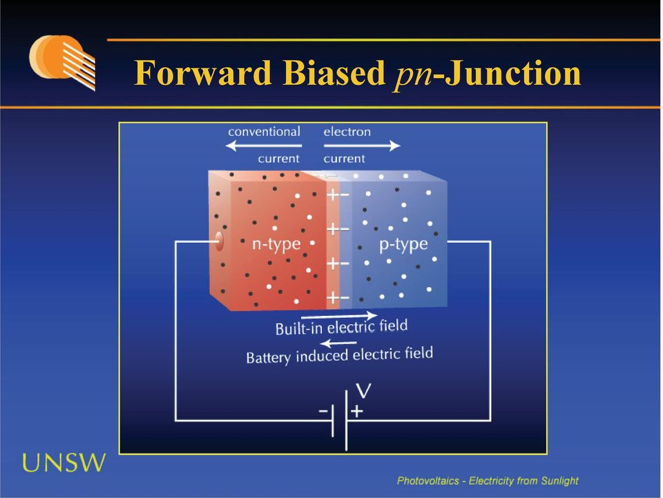
7 These opposing flows eventually reach a stable equilibrium with the number of electrons flowing due to diffusion exactly balancing the number of electrons flowing back due to the electric field. The net flow of electrons across the junction is zero and the net flow of holes across the junction is also zero. This begs the question, "If there is no net current flowing, of what use is it?" Although there is no net flow of current across the junction there has been established an electric field at the junction and it is this electric field that is the basis of the operation of diodes, transistors and solar cells. Depletion Region Within the depletion region, there are very few mobile electrons and holes. It is "depleted" of mobile charges, leaving only the fixed charges associated with the dopant atoms. As a result, the depletion region is highly resistive and now behaves as if it were pure crystalline silicon: as a nearly perfect insulator. The resistance of the depletion region can be modified by "adding" an external electric field to the "built-in" electric field. If the "added" electric field is in the same direction as the "built-in" electric field, the depletion region's resistance will become greater. If the "added" electric field is opposite in direction to the "built-in" electric field, the depletion region's resistance will become smaller. The depletion region can therefore be considered to operate as a voltage-controlled resistor. Forward Bias If a positive voltage is applied to the p-type side and a negative voltage to the n-type side, current can flow (depending upon the magnitude of the applied voltage). This configuration is called "Forward Biased" (see Figure 5). At the p-n junction, the "built-in" electric field and the applied electric field are in opposite directions. When these two fields add, the resultant field at the junction is smaller in magnitude than the magnitude of the original "built-in" electric field. This results in a thinner, less resistive depletion region. If the applied voltage is large enough, the depletion region's resistance becomes negligible. In silicon, this occurs at about 0.6 volts forward bias. From 0 to 0.6 volts, there is still considerable resistance due to the depletion region. Above 0.6 volts, the depletion region's resistance is very small and current flows virtually unimpeded. 19

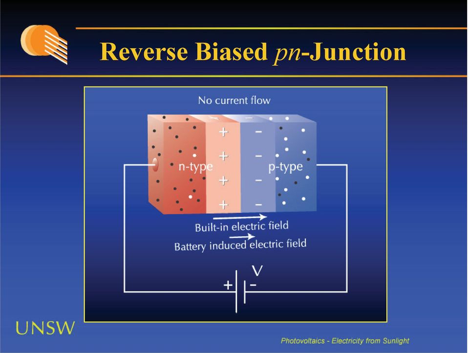
8 Figure 5 Forward bias of the p-n junction. Reverse Bias If a negative voltage is applied to the p-type side and a positive voltage to the n-type side, no (or exceptionally small) current flows. This configuration is called "Reverse Biased" (see Figure 6). Figure 6 Reverse bias of the p-n Junction. 20
.")
9 At the p-n junction, the "built-in" electric field and the applied electric field are in the same direction. When these two fields add, the resultant larger electric field is in the same direction as the "built in" electric field and this creates a thicker, more resistive depletion region. If the applied voltage becomes larger, the depletion region becomes thicker and more resistive. In reality, some current will still flow through this resistance, but the resistance is so high that the current may be considered to be zero. As the applied reverse bias voltage becomes larger, the current flow will saturate at a constant but very small value. This is approximately amperes per cm 2 of p-n junction area. Figure 7 IV curve of the silicon p-n junction diode. The current-voltage relation or IV curve of a silicon p-n junction is shown in Figure 7. In reverse bias, the p-n junction exhibits extreme electrical resistance and only a very small current flows. If the reverse bias voltage becomes too large then the junction will breakdown and current will flow. It is possible to design silicon p-n junctions in such a way that the breakdown voltage is at a specific desired value. Such p-n junctions are called zener diodes and are used as voltage references or overvoltage protectors in electrical cir- In forward bias, the p-n junction exhibits an exponential lowering of resistance with applied voltage. From 0 to 0.5 volts, the silicon p-n junction is quite resistive. When the applied voltage approaches 0.6 volts, the exponential nature of the junction causes the resistance to drop dramatically. The silicon p-n junction diode appears to be an electrical switch that "turns on" when 0.6 volts is applied. Because electrical current flows only when it is forward biased, the diode appears to be an electrical one-way valve. 21

10 How a Solar Cell Works Now it can be seen what happens inside a solar cell. Most solar cells are essentially large area p-n junctions. When light shines on them they can generate current and voltage. The reason this can happen is because of the "built-in" electric field at the junction of the p-type and n-type material. First consider what happens if a silicon solar cell (which is a p-n junction) has a low resistance wire connected externally between the p and n contact. In the dark a solar cell will produce no current. If, however, light shines on the solar cell then current will flow through the wire, from the p-type side to the n-type side (conventional current). How It Happens The light has enough energy to break some of the chemical bonds of the silicon crystal. What that means is that electrons, which are normally involved in a silicon bond, are excited by the light into a higher energy state and the bond is broken. Not all of the bonds are broken otherwise the silicon would melt! The sun's light intensity on earth is strong enough to break about 1 bond for every 100 million silicon atoms in the solar cell. So the solar cell doesn't melt under normal conditions. The excited electrons are now like the electrons from phosphorus dopant atoms - they are free to move through the material. Similarly, the broken bonds created by the light act as holes - just like the missing electrons in bonds between silicon and boron atoms - and these holes are also free to move throughout the material. What goes up, however, must eventually come down! Electrons and holes created in this way are physically near each other: for every electron excited by the light there is a corresponding hole generated. These electrons and holes can remain excited only for a short period of time. In a process called recombination, excited electrons stray too close to holes and the two fall back into bonded positions. When this happens the pair's electrical energy is lost as heat. If there is too much recombination, the solar cell won't work very well. Current flow from a Solar Cell The electrons and holes excited by light shining on the solar cell occur throughout the volume of the material, in the p-region, the n-region and at the junction region where there is a built-in electric field. It is easiest to understand the flow of current by first considering electrons and holes that are excited by the light in the junction region. Because of the built-in electric field, the electrons are attracted towards the positive charge on the n-type material side. Similarly, the holes are attracted to the negative charge on the p-type material side. This separation of charges causes a current to flow across the junction. The direction of the current flow (conventional current) is the same as the motion of the holes (as they are positively charged). That is, the current flows across the junction from the n-type side to the p-type side. 22
.")
11 Similarly, electrons and holes, which are far away from the junction, can be separated by the built-in electric field if they can find their way towards the junction before they recombine. This occurs simply because the electrons and holes will randomly diffuse throughout the material. If they manage to randomly wander into the built-in electric field region, before recombining, then they will contribute to the current flowing across the junction. These charges will also cause flow of electrons through the external wire. Electric current can be measured by simply attaching a current meter in series with a solar cell. Because the resistance across the wire and the current meter is very low, there will be essentially no voltage across the solar cell, but current can flow. This is called the shortcircuit current. The Voltage of a Solar Cell In the situation described above there is current flowing through the wire and meter but there isn't any voltage (yet!). Power can be extracted from the solar cell only if it can produce both voltage and current. What happens if the wire is cut? In this case, there is no pathway for any light generated current to flow outside of the solar cell. Separation of electrons and holes, however, keeps happening inside the solar cell. Electrons are being pushed over toward the n-type side and holes are being pushed over towards the p-type side (if they manage to wander near the junction without first recombining). When the wire is cut, there is no external circuit for these charges to flow through. Instead, the flow of electrons into the n-type side and the flow of holes into the p-type side, causes a voltage to build up across the solar cell - positive voltage on the p-type side and negative voltage on the n-type side. There is now a voltage across the solar cell, however, there is no current flowing from the solar cell. The "opencircuit voltage" is measured by placing a voltmeter across the illuminated solar cell. For a silicon solar cell, it will measure about 0.6 volts in strong sunlight. A Closer Look at the Open-Circuit voltage If a p-n junction has an external forward bias voltage applied across it, a current will flow through the junction of the solar cell from the p-type side to the n-type side (conventional current). When an open circuit solar cell is illuminated, the light generated electrons and holes that wander near the junction will be separated by the built-in electric field. The electrons will be pushed into the n-type region and the holes will be pushed into the p-type region. A light generated flow of current through the junction is opposite in direction to a forward bias flow of current. In an illuminated open circuit solar cell there is a constant value of light generated electrons and holes flowing across the junction and into the corresponding p-type and n-type regions. The light generated current depends only on how intense the sunlight is and how much recombination occurs within the solar cell. This collection of charge creates a voltage across the solar cell. It could be imagined that this separation of charge would continue indefinitely with the result being that the voltage across the solar cell becomes infinite. 23

12 Something happens, however, to limit the voltage. The solar cell is now forward biased and just as for the p-n junction in the dark, current flows across the junction from the p-type side to the n-type side. This forward bias current is in the opposite direction to the light generated current described above. Both currents are flowing simultaneously. As the voltage across the solar cell builds up, it eventually reaches a point where the forward bias current exactly balances the light generated current. These two internal currents flow inside the solar cell cancelling each other out. The voltage at which this occurs is called the "open-circuit voltage". For a silicon solar cell it is typically 0.6 volts in bright sunshine. Getting Power from a Solar Cell For short-circuit conditions there is a low resistance wire connected between the solar cell contacts resulting in a current flowing but no generated voltage. If the wire is cut, the solar cell is now open-circuited resulting in a voltage being generated but no current flowing. In order to get useful power out of a solar cell there needs to be a resistance between the two contacts that has just the right value. If the resistance is too low, then there will be mostly current coming from the solar cell and very little voltage generated. If too high a resistance is connected across the contacts there will be mostly voltage generated and very little current coming out of the solar cell. Only when the right resistance is connected across the solar cell will there be an optimal voltage generated with an optimal current flowing. With this value of resistance across the solar cell, the maximum electrical energy available from the solar cell is being delivered to the resistor. Under these conditions, the solar cell is said to be operating at its "Maximum Power Point". For Large Amounts of Power In order to generate large amounts of power from solar cells all that is needed is to wire many solar cells together. Collectively, the cells can generate enough power to do useful work. In fact, it is possible to wire together enough solar cells to form a great big solar cell power station. The electricity generated could then be used to power anything from a single light bulb to a large electric train, and with even more solar cells in the circuit, it would be possible to power an entire city! 24

13 The Silicon Solar Cell

14 Direction of Current Flow

15 Two Pieces of Doped Silicon

16 n-type and p-type Joined

17 Diffusion via Random Motion

18 Diffusion & Built-In Currents

19 Forward Biased pn-junction
20 Reverse Biased pn-junction
21 Characteristics of the pn-junction
3. Diodes and Diode Circuits. 3. Diodes and Diode Circuits TLT-8016 Basic Analog Circuits 2005/2006 1
 3. Diodes and Diode Circuits 3. Diodes and Diode Circuits TLT-8016 Basic Analog Circuits 2005/2006 1 3.1 Diode Characteristics Small-Signal Diodes Diode: a semiconductor device, which conduct the current
Semiconductors, diodes, transistors
 Semiconductors, diodes, transistors (Horst Wahl, QuarkNet presentation, June 2001) Electrical conductivity! Energy bands in solids! Band structure and conductivity Semiconductors! Intrinsic semiconductors!
Yrd. Doç. Dr. Aytaç Gören
 H2 - AC to DC Yrd. Doç. Dr. Aytaç Gören ELK 2018 - Contents W01 Basic Concepts in Electronics W02 AC to DC Conversion W03 Analysis of DC Circuits W04 Transistors and Applications (H-Bridge) W05 Op Amps
Crystalline solids. A solid crystal consists of different atoms arranged in a periodic structure.
 Crystalline solids A solid crystal consists of different atoms arranged in a periodic structure. Crystals can be formed via various bonding mechanisms: Ionic bonding Covalent bonding Metallic bonding Van
Characteristic curves of a solar cell
 Related Topics Semi-conductor, p-n junction, energy-band diagram, Fermi characteristic energy level, diffusion potential, internal resistance, efficiency, photo-conductive effect, acceptors, donors, valence
Solid-State Physics: The Theory of Semiconductors (Ch. 10.6-10.8) SteveSekula, 30 March 2010 (created 29 March 2010)
 SteveSekula, 30 March 2010 (created 29 March 2010)") Modern Physics (PHY 3305) Lecture Notes Modern Physics (PHY 3305) Lecture Notes Solid-State Physics: The Theory of Semiconductors (Ch. 10.6-10.8) SteveSekula, 30 March 2010 (created 29 March 2010) Review
Modern Physics (PHY 3305) Lecture Notes Modern Physics (PHY 3305) Lecture Notes Solid-State Physics: The Theory of Semiconductors (Ch. 10.6-10.8) SteveSekula, 30 March 2010 (created 29 March 2010) Review
David L. Senasack June, 2006 Dale Jackson Career Center, Lewisville Texas. The PN Junction
 David L. Senasack June, 2006 Dale Jackson Career Center, Lewisville Texas The PN Junction Objectives: Upon the completion of this unit, the student will be able to; name the two categories of integrated
Semiconductor I. Semiconductors. germanium. silicon
 Basic Electronics Semiconductor I Materials that permit flow of electrons are called conductors (e.g., gold, silver, copper, etc.). Materials that block flow of electrons are called insulators (e.g., rubber,
From Nano-Electronics and Photonics to Renewable Energy
 From Nano-Electronics and Photonics to Renewable Energy Tom Smy Department of Electronics, Carleton University Questions are welcome! OUTLINE Introduction: to EE and Engineering Physics Renewable Energy
Solar Energy Discovery Lab
 Solar Energy Discovery Lab Objective Set up circuits with solar cells in series and parallel and analyze the resulting characteristics. Introduction A photovoltaic solar cell converts radiant (solar) energy
Solid State Detectors = Semi-Conductor based Detectors
 Solid State Detectors = Semi-Conductor based Detectors Materials and their properties Energy bands and electronic structure Charge transport and conductivity Boundaries: the p-n junction Charge collection
FUNDAMENTAL PROPERTIES OF SOLAR CELLS
 FUNDAMENTAL PROPERTIES OF SOLAR CELLS January 31, 2012 The University of Toledo, Department of Physics and Astronomy SSARE, PVIC Principles and Varieties of Solar Energy (PHYS 4400) and Fundamentals of
The Physics of Energy sources Renewable sources of energy. Solar Energy
 The Physics of Energy sources Renewable sources of energy Solar Energy B. Maffei Bruno.maffei@manchester.ac.uk Renewable sources 1 Solar power! There are basically two ways of using directly the radiative
PS-6.2 Explain the factors that determine potential and kinetic energy and the transformation of one to the other.
 PS-6.1 Explain how the law of conservation of energy applies to the transformation of various forms of energy (including mechanical energy, electrical energy, chemical energy, light energy, sound energy,
Solar Cell Parameters and Equivalent Circuit
 9 Solar Cell Parameters and Equivalent Circuit 9.1 External solar cell parameters The main parameters that are used to characterise the performance of solar cells are the peak power P max, the short-circuit
Theory of Transistors and Other Semiconductor Devices
 Theory of Transistors and Other Semiconductor Devices 1. SEMICONDUCTORS 1.1. Metals and insulators 1.1.1. Conduction in metals Metals are filled with electrons. Many of these, typically one or two per
Photovoltaics photo volt Photovoltaic Cells Crystalline Silicon Cells Photovoltaic Systems
 1 Photovoltaics Photovoltaic (PV) materials and devices convert sunlight into electrical energy, and PV cells are commonly known as solar cells. Photovoltaics can literally be translated as light-electricity.
Solar Photovoltaic (PV) Cells
 Cells") Solar Photovoltaic (PV) Cells A supplement topic to: Mi ti l S Micro-optical Sensors - A MEMS for electric power generation Science of Silicon PV Cells Scientific base for solar PV electric power generation
Solar Photovoltaic (PV) Cells A supplement topic to: Mi ti l S Micro-optical Sensors - A MEMS for electric power generation Science of Silicon PV Cells Scientific base for solar PV electric power generation
BASIC ELECTRONICS TRANSISTOR THEORY. December 2011
 AM 5-204 BASIC ELECTRONICS TRANSISTOR THEORY December 2011 DISTRIBUTION RESTRICTION: Approved for Public Release. Distribution is unlimited. DEPARTMENT OF THE ARMY MILITARY AUXILIARY RADIO SYSTEM FORT
Here Comes the Sun. Provided by TryEngineering - www.tryengineering.org
 Provided by TryEngineering - Lesson Focus Lesson focuses on solar panel design, and its application in the standard calculator. It explores how both solar panels and calculators operate and explores simple
ENEE 313, Spr 09 Midterm II Solution
 ENEE 313, Spr 09 Midterm II Solution PART I DRIFT AND DIFFUSION, 30 pts 1. We have a silicon sample with non-uniform doping. The sample is 200 µm long: In the figure, L = 200 µm= 0.02 cm. At the x = 0
Special-Purpose Diodes
 7 Special-Purpose Diodes 7.1 Zener Diode 7.2 Light-Emitting Diode (LED) 7.3 LED Voltage and Current 7.4 Advantages of LED 7.5 Multicolour LEDs 7.6 Applications of LEDs 7.7 Photo-diode 7.8 Photo-diode operation
Information sheet. 1) Solar Panels - Basics. 2) Solar Panels Functionality
 Solar Panels - Basics. 2) Solar Panels Functionality") 1) Solar Panels - Basics A solar cell, sometimes called a photovoltaic cell, is a device that converts light energy into electrical energy. A single solar cell creates a very small amount of energy so
1) Solar Panels - Basics A solar cell, sometimes called a photovoltaic cell, is a device that converts light energy into electrical energy. A single solar cell creates a very small amount of energy so
Modern Construction Materials Prof. Ravindra Gettu Department of Civil Engineering Indian Institute of Technology, Madras
 Modern Construction Materials Prof. Ravindra Gettu Department of Civil Engineering Indian Institute of Technology, Madras Module - 2 Lecture - 2 Part 2 of 2 Review of Atomic Bonding II We will continue
ELECTRICAL FUNDAMENTALS
 General Electricity is a form of energy called electrical energy. It is sometimes called an "unseen" force because the energy itself cannot be seen, heard, touched, or smelled. However, the effects of
What is Solar? The word solar is derived from the Latin word sol (the sun, the Roman sun god) and refers to things and methods that relate to the sun.
 and refers to things and methods that relate to the sun.") What is Solar? The word solar is derived from the Latin word sol (the sun, the Roman sun god) and refers to things and methods that relate to the sun. What is the solar industry? The solar industry is
What is Solar? The word solar is derived from the Latin word sol (the sun, the Roman sun god) and refers to things and methods that relate to the sun. What is the solar industry? The solar industry is
Lecture 2 - Semiconductor Physics (I) September 13, 2005
 September 13, 2005") 6.012 - Microelectronic Devices and Circuits - Fall 2005 Lecture 2-1 Lecture 2 - Semiconductor Physics (I) September 13, 2005 Contents: 1. Silicon bond model: electrons and holes 2. Generation and recombination
6.012 - Microelectronic Devices and Circuits - Fall 2005 Lecture 2-1 Lecture 2 - Semiconductor Physics (I) September 13, 2005 Contents: 1. Silicon bond model: electrons and holes 2. Generation and recombination
Project 2B Building a Solar Cell (2): Solar Cell Performance
: Solar Cell Performance") April. 15, 2010 Due April. 29, 2010 Project 2B Building a Solar Cell (2): Solar Cell Performance Objective: In this project we are going to experimentally measure the I-V characteristics, energy conversion
April. 15, 2010 Due April. 29, 2010 Project 2B Building a Solar Cell (2): Solar Cell Performance Objective: In this project we are going to experimentally measure the I-V characteristics, energy conversion
ELG4126: Photovoltaic Materials. Based Partially on Renewable and Efficient Electric Power System, Gilbert M. Masters, Wiely
 ELG4126: Photovoltaic Materials Based Partially on Renewable and Efficient Electric Power System, Gilbert M. Masters, Wiely Introduction A material or device that is capable of converting the energy contained
Conduction in Semiconductors
 Chapter 1 Conduction in Semiconductors 1.1 Introduction All solid-state devices, e.g. diodes and transistors, are fabricated from materials known as semiconductors. In order to understand the operation
Lecture 15 - application of solid state materials solar cells and photovoltaics. Copying Nature... Anoxygenic photosynthesis in purple bacteria
 Lecture 15 - application of solid state materials solar cells and photovoltaics. Copying Nature... Anoxygenic photosynthesis in purple bacteria Simple example, but still complicated... Photosynthesis is
Figure 1. Diode circuit model
 Semiconductor Devices Non-linear Devices Diodes Introduction. The diode is two terminal non linear device whose I-V characteristic besides exhibiting non-linear behavior is also polarity dependent. The
COURSE: PHYSICS DEGREE: COMPUTER ENGINEERING year: 1st SEMESTER: 1st
 COURSE: PHYSICS DEGREE: COMPUTER ENGINEERING year: 1st SEMESTER: 1st WEEKLY PROGRAMMING WEE K SESSI ON DESCRIPTION GROUPS GROUPS Special room for LECTU PRAC session RES TICAL (computer classroom, audiovisual
Type of Chemical Bonds
 Type of Chemical Bonds Covalent bond Polar Covalent bond Ionic bond Hydrogen bond Metallic bond Van der Waals bonds. Covalent Bonds Covalent bond: bond in which one or more pairs of electrons are shared
High Resolution Spatial Electroluminescence Imaging of Photovoltaic Modules
 High Resolution Spatial Electroluminescence Imaging of Photovoltaic Modules Abstract J.L. Crozier, E.E. van Dyk, F.J. Vorster Nelson Mandela Metropolitan University Electroluminescence (EL) is a useful
05 Bipolar Junction Transistors (BJTs) basics
 basics") The first bipolar transistor was realized in 1947 by Brattain, Bardeen and Shockley. The three of them received the Nobel prize in 1956 for their invention. The bipolar transistor is composed of two PN
The first bipolar transistor was realized in 1947 by Brattain, Bardeen and Shockley. The three of them received the Nobel prize in 1956 for their invention. The bipolar transistor is composed of two PN
Name Class Date. What is ionic bonding? What happens to atoms that gain or lose electrons? What kinds of solids are formed from ionic bonds?
 CHAPTER 1 2 Ionic Bonds SECTION Chemical Bonding BEFORE YOU READ After you read this section, you should be able to answer these questions: What is ionic bonding? What happens to atoms that gain or lose
Field-Effect (FET) transistors
 transistors") Field-Effect (FET) transistors References: Hayes & Horowitz (pp 142-162 and 244-266), Rizzoni (chapters 8 & 9) In a field-effect transistor (FET), the width of a conducting channel in a semiconductor and,
Field-Effect (FET) transistors References: Hayes & Horowitz (pp 142-162 and 244-266), Rizzoni (chapters 8 & 9) In a field-effect transistor (FET), the width of a conducting channel in a semiconductor and,
Why is it renewable? Well, the sun will always be there for us, and we can use as much of the sun s energy as we want and it will never run out.
 6. Solar Energy So far we have been looking at how to reduce CO 2 emissions by cutting down on our use of fossil fuels. Now let s look at getting renewable energy from the sun. Why is it renewable? Well,
LAB IV. SILICON DIODE CHARACTERISTICS
 LAB IV. SILICON DIODE CHARACTERISTICS 1. OBJECTIVE In this lab you are to measure I-V characteristics of rectifier and Zener diodes in both forward and reverse-bias mode, as well as learn to recognize
Amplifier Teaching Aid
 Amplifier Teaching Aid Table of Contents Amplifier Teaching Aid...1 Preface...1 Introduction...1 Lesson 1 Semiconductor Review...2 Lesson Plan...2 Worksheet No. 1...7 Experiment No. 1...7 Lesson 2 Bipolar
Diode Circuits. Operating in the Reverse Breakdown region. (Zener Diode)
") Diode Circuits Operating in the Reverse Breakdown region. (Zener Diode) In may applications, operation in the reverse breakdown region is highly desirable. The reverse breakdown voltage is relatively insensitive
Diode Circuits Operating in the Reverse Breakdown region. (Zener Diode) In may applications, operation in the reverse breakdown region is highly desirable. The reverse breakdown voltage is relatively insensitive
Fundamentals of Microelectronics
 Fundamentals of Microelectronics CH1 Why Microelectronics? CH2 Basic Physics of Semiconductors CH3 Diode Circuits CH4 Physics of Bipolar Transistors CH5 Bipolar Amplifiers CH6 Physics of MOS Transistors
Lab 1 Diode Characteristics
 Lab 1 Diode Characteristics Purpose The purpose of this lab is to study the characteristics of the diode. Some of the characteristics that will be investigated are the I-V curve and the rectification properties.
SOLAR CELLS From light to electricity
 SOLAR CELLS From light to electricity Solar Impulse uses nothing but light to power its motors. The effect of light on the material in solar panels allows them to produce the electricity that is needed
Introduction OLEDs OTFTs OPVC Summary. Organic Electronics. Felix Buth. Walter Schottky Institut, TU München. Joint Advanced Student School 2008
 Felix Buth Joint Advanced Student School 2008 Outline 1 Introduction Difference organic/inorganic semiconductors From molecular orbitals to the molecular crystal 2 Organic Light Emitting Diodes Basic Principals
AMPLIFIERS BJT BJT TRANSISTOR. Types of BJT BJT. devices that increase the voltage, current, or power level
 AMPLFERS Prepared by Engr. JP Timola Reference: Electronic Devices by Floyd devices that increase the voltage, current, or power level have at least three terminals with one controlling the flow between
Measuring Silicon and Germanium Band Gaps using Diode Thermometers
 Measuring Silicon and Germanium Band Gaps using Diode Thermometers Haris Amin Department of Physics, Wabash College, Crawfordsville, IN 47933 (Dated: April 11, 2007) This paper reports the band gaps of
CONTENTS. Preface. 1.1.2. Energy bands of a crystal (intuitive approach)
") CONTENTS Preface. Energy Band Theory.. Electron in a crystal... Two examples of electron behavior... Free electron...2. The particle-in-a-box approach..2. Energy bands of a crystal (intuitive approach)..3.
CONTENTS Preface. Energy Band Theory.. Electron in a crystal... Two examples of electron behavior... Free electron...2. The particle-in-a-box approach..2. Energy bands of a crystal (intuitive approach)..3.
List the 3 main types of subatomic particles and indicate the mass and electrical charge of each.
 Basic Chemistry Why do we study chemistry in a biology course? All living organisms are composed of chemicals. To understand life, we must understand the structure, function, and properties of the chemicals
Basic Electronics Prof. Dr. Chitralekha Mahanta Department of Electronics and Communication Engineering Indian Institute of Technology, Guwahati
 Basic Electronics Prof. Dr. Chitralekha Mahanta Department of Electronics and Communication Engineering Indian Institute of Technology, Guwahati Module: 2 Bipolar Junction Transistors Lecture-2 Transistor
The MOSFET Transistor
 The MOSFET Transistor The basic active component on all silicon chips is the MOSFET Metal Oxide Semiconductor Field Effect Transistor Schematic symbol G Gate S Source D Drain The voltage on the gate controls
3.- What atom s particle moves through a conductor material? 4.- Which are the electric components of an elemental electric circuit?
 1.- What is electricity? 2.- Write down the name of the atom s particles. 3.- What atom s particle moves through a conductor material? 4.- Which are the electric components of an elemental electric circuit?
Current, Resistance and Electromotive Force. Young and Freedman Chapter 25
 Current, Resistance and Electromotive Force Young and Freedman Chapter 25 Electric Current: Analogy, water flowing in a pipe H 2 0 gallons/minute Flow Rate is the NET amount of water passing through a
Solar Matters III Teacher Page
 Solar Matters III Teacher Page Solar Powered System - 2 Student Objective Given a photovoltaic system will be able to name the component parts and describe their function in the PV system. will be able
Chapter 4, Lesson 4: Energy Levels, Electrons, and Covalent Bonding
 Chapter 4, Lesson 4: Energy Levels, Electrons, and Covalent Bonding Key Concepts The electrons on the outermost energy level of the atom are called valence electrons. The valence electrons are involved
 Solar Power for Agriculture and Our Experiences at the Middlesex County EARTH Center Rutgers Cooperative Extension William T. Hlubik Agricultural and Resource Management Agent Rutgers Cooperative Extension
High Open Circuit Voltage of MQW Amorphous Silicon Photovoltaic Structures
 High Open Circuit Voltage of MQW Amorphous Silicon Photovoltaic Structures ARGYRIOS C. VARONIDES Physics and EE Department University of Scranton 800 Linden Street, Scranton PA, 18510 United States Abstract:
SOLAR ENERGY. Overview: Objectives: Targeted Alaska Performance Standards for the High School Graduation Qualifying Exam:
 Overview: In this lesson, students investigate energy transfer and photovoltaic (PV) cells through hands-on experiments. Students explore the impact of intensity and angle of light on the power produced
ELEC 3908, Physical Electronics, Lecture 15. BJT Structure and Fabrication
 ELEC 3908, Physical Electronics, Lecture 15 Lecture Outline Now move on to bipolar junction transistor (BJT) Strategy for next few lectures similar to diode: structure and processing, basic operation,
Diodes have an arrow showing the direction of the flow.
 The Big Idea Modern circuitry depends on much more than just resistors and capacitors. The circuits in your computer, cell phone, Ipod depend on circuit elements called diodes, inductors, transistors,
Chapter 13: Electric Circuits
 Chapter 13: Electric Circuits 1. A household circuit rated at 120 Volts is protected by a fuse rated at 15 amps. What is the maximum number of 100 watt light bulbs which can be lit simultaneously in parallel
Table of Contents 1. Introduction 2. Electrical Fundamentals Electron Theory Matter 4 MOLECULE
 Table of Contents 1. Introduction 3 2. Electrical Fundamentals 4 Electron Theory 4 Matter 4 MOLECULE 5 The atom 6 Atom construction 7 Electrical charges 11 Balanced atoms 12 Ions 13 Electron orbits 15
Junction FETs. FETs. Enhancement Not Possible. n p n p n p
 A11 An Introduction to FETs Introduction The basic principle of the field-effect transistor (FET) has been known since J. E. Lilienfeld s patent of 1925. The theoretical description of a FET made by hockley
Fundamentals of Microelectronics
 Fundamentals of Microelectronics H1 Why Microelectronics? H2 Basic Physics of Semiconductors H3 Diode ircuits H4 Physics of Bipolar ransistors H5 Bipolar Amplifiers H6 Physics of MOS ransistors H7 MOS
Graphene a material for the future
 Graphene a material for the future by Olav Thorsen What is graphene? What is graphene? Simply put, it is a thin layer of pure carbon What is graphene? Simply put, it is a thin layer of pure carbon It has
STUDY GUIDE: ELECTRICITY AND MAGNETISM
 319 S. Naperville Road Wheaton, IL 60187 www.questionsgalore.net Phone: (630) 580-5735 E-Mail: info@questionsgalore.net Fax: (630) 580-5765 STUDY GUIDE: ELECTRICITY AND MAGNETISM An atom is made of three
Untitled Document. 1. Which of the following best describes an atom? 4. Which statement best describes the density of an atom s nucleus?
 Name: Date: 1. Which of the following best describes an atom? A. protons and electrons grouped together in a random pattern B. protons and electrons grouped together in an alternating pattern C. a core
Forms of Energy. Freshman Seminar
 Forms of Energy Freshman Seminar Energy Energy The ability & capacity to do work Energy can take many different forms Energy can be quantified Law of Conservation of energy In any change from one form
Time allowed: 1 hour 45 minutes
 GCSE PHYSICS Foundation Tier Paper 1F F Specimen 2018 Time allowed: 1 hour 45 minutes Materials For this paper you must have: a ruler a calculator the Physics Equation Sheet (enclosed). Instructions Answer
Diodes and Transistors
 Diodes What do we use diodes for? Diodes and Transistors protect circuits by limiting the voltage (clipping and clamping) turn AC into DC (voltage rectifier) voltage multipliers (e.g. double input voltage)
GenTech Practice Questions
 GenTech Practice Questions Basic Electronics Test: This test will assess your knowledge of and ability to apply the principles of Basic Electronics. This test is comprised of 90 questions in the following
Wires & Connections Component Circuit Symbol Function of Component. Power Supplies Component Circuit Symbol Function of Component
 Lista Dei Simboli Dei Circuiti Per i Componenti Elettronici Wires & Connections Wire Wires joined Wires not joined To pass current very easily from one part of a circuit to another. A 'blob' should be
Circuit symbol. Each of the cells has a potential difference of 1.5 volts. Figure 1. Use the correct answer from the box to complete the sentence.
 Q.(a) Draw one line from each circuit symbol to its correct name. Circuit symbol Name Diode Light-dependent resistor (LDR) Lamp Light-emitting diode (LED) (3) Figure shows three circuits. The resistors
V-I CHARACTERISTICS OF DIODE
 V-I CHARACTERISTICS OF DIODE RAVITEJ UPPU 1 1. Aim We try to see the Voltage-Current realtion in Diodes and compare the difference between various types of diodes including Zener Diode. 2. Theory The diode
7. The current voltage characteristic of electric conductors
 KL 7. The current voltage characteristic of electric conductors 7.1 ntroduction The purpose of the present laboratory is to measure the current voltage characteristic of different conducting components.
Series and Parallel Circuits
 Series and Parallel Circuits Direct-Current Series Circuits A series circuit is a circuit in which the components are connected in a line, one after the other, like railroad cars on a single track. There
Energy Transfer in a Flash-Light. (Teacher Copy)
") Energy Transfer in a Flash-Light (Teacher Copy) Florida Sunshine State Standards Benchmark: SC.B. 1.3.1 AA The student identifies forms of energy and explains that they can be measured and compared. (Also
Energy Transfer in a Flash-Light (Teacher Copy) Florida Sunshine State Standards Benchmark: SC.B. 1.3.1 AA The student identifies forms of energy and explains that they can be measured and compared. (Also
What is solar power? Solar power uses the suns energy and converts it into an electric current.
 General Solar FAQs: What is solar power? Solar power uses the suns energy and converts it into an electric current. What is a solar cell? A solar cell, also called a photovoltaic (PV) cell, is the smallest
2 A bank account for electricity II: flows and taxes
 PHYS 189 Lecture problems outline Feb 3, 2014 Resistors and Circuits Having introduced capacitors, we now expand our focus to another very important component of a circuit resistors. This entails more
Chapter 2 The Chemical Context of Life
 Chapter 2 The Chemical Context of Life Multiple-Choice Questions 1) About 25 of the 92 natural elements are known to be essential to life. Which four of these 25 elements make up approximately 96% of living
ELECTRICAL CONDUCTION
 Chapter 12: Electrical Properties Learning Objectives... How are electrical conductance and resistance characterized? What are the physical phenomena that distinguish conductors, semiconductors, and insulators?
Matter, Materials, Crystal Structure and Bonding. Chris J. Pickard
 Matter, Materials, Crystal Structure and Bonding Chris J. Pickard Why should a theorist care? Where the atoms are determines what they do Where the atoms can be determines what we can do Overview of Structure
The API Solar Car Manual 2015
 The API Solar Car Manual 2015 STELR API Solar Car Manual www.stelr.org.au 1 of 18 Contents Introduction... 3 Student tasks... 3 Make the fastest car... 3 Make the most powerful car... 3 Make the most efficient
1. The diagram below represents magnetic lines of force within a region of space.
 1. The diagram below represents magnetic lines of force within a region of space. 4. In which diagram below is the magnetic flux density at point P greatest? (1) (3) (2) (4) The magnetic field is strongest
Project Report on Solar Charger Circuit using IC LM317
 Project Report on Solar Charger Circuit using IC LM317 Prepared by: Neha Kondekar Undergraduate 1 st Year, Indian Institute of Science, Bangalore Guided By: Amit K Gupta, Prof. Navakant Bhat Centre for
THE CURRENT-VOLTAGE CHARACTERISTICS OF AN LED AND A MEASUREMENT OF PLANCK S CONSTANT Physics 258/259
 DSH 2004 THE CURRENT-VOLTAGE CHARACTERISTICS OF AN LED AND A MEASUREMENT OF PLANCK S CONSTANT Physics 258/259 I. INTRODUCTION Max Planck (1858-1947) was an early pioneer in the field of quantum physics.
An Approach to Alternative Energy Solutions for the Home
 An Approach to Alternative Energy Solutions for the Home By Robert Rasmussen An Engineering Project Submitted to the Graduate Faculty of Rensselaer Polytechnic Institute in Partial Fulfillment of the Requirements
DIODE CIRCUITS LABORATORY. Fig. 8.1a Fig 8.1b
 DIODE CIRCUITS LABORATORY A solid state diode consists of a junction of either dissimilar semiconductors (pn junction diode) or a metal and a semiconductor (Schottky barrier diode). Regardless of the type,
CHAPTER - 1. Chapter ONE: WAVES CHAPTER - 2. Chapter TWO: RAY OPTICS AND OPTICAL INSTRUMENTS. CHAPTER - 3 Chapter THREE: WAVE OPTICS PERIODS PERIODS
 BOARD OF INTERMEDIATE EDUCATION, A.P., HYDERABAD REVISION OF SYLLABUS Subject PHYSICS-II (w.e.f 2013-14) Chapter ONE: WAVES CHAPTER - 1 1.1 INTRODUCTION 1.2 Transverse and longitudinal waves 1.3 Displacement
Atoms and Elements. Outline Atoms Orbitals and Energy Levels Periodic Properties Homework
 Atoms and the Periodic Table The very hot early universe was a plasma with cationic nuclei separated from negatively charged electrons. Plasmas exist today where the energy of the particles is very high,
The rate of change of velocity with respect to time. The average rate of change of distance/displacement with respect to time.
 H2 PHYSICS DEFINITIONS LIST Scalar Vector Term Displacement, s Speed Velocity, v Acceleration, a Average speed/velocity Instantaneous Velocity Newton s First Law Newton s Second Law Newton s Third Law
W04 Transistors and Applications. Yrd. Doç. Dr. Aytaç Gören
 W04 Transistors and Applications W04 Transistors and Applications ELK 2018 - Contents W01 Basic Concepts in Electronics W02 AC to DC Conversion W03 Analysis of DC Circuits (self and condenser) W04 Transistors
Elements in the periodic table are indicated by SYMBOLS. To the left of the symbol we find the atomic mass (A) at the upper corner, and the atomic num
 at the upper corner, and the atomic num") . ATOMIC STRUCTURE FUNDAMENTALS LEARNING OBJECTIVES To review the basics concepts of atomic structure that have direct relevance to the fundamental concepts of organic chemistry. This material is essential
. ATOMIC STRUCTURE FUNDAMENTALS LEARNING OBJECTIVES To review the basics concepts of atomic structure that have direct relevance to the fundamental concepts of organic chemistry. This material is essential
DARK CURRENT-VOLTAGE MEASUREMENTS ON PHOTOVOLTAIC MODULES AS A DIAGNOSTIC OR MANUFACTURING TOOL
 t DARK CURRENT-VOLTAGE MEASUREMENTS ON PHOTOVOLTAC MODULES AS A DAGNOSTC OR MANUFACTURNG TOOL D. L. King, 6. R. Hansen, J. A. Kratochvil, and M. A. Quintana Sandia National Laboratories, Albuquerque, NM
5s Solubility & Conductivity
 5s Solubility & Conductivity OBJECTIVES To explore the relationship between the structures of common household substances and the kinds of solvents in which they dissolve. To demonstrate the ionic nature
MOS (metal-oxidesemiconductor) 李 2003/12/19
 李 2003/12/19") MOS (metal-oxidesemiconductor) 李 2003/12/19 Outline Structure Ideal MOS The surface depletion region Ideal MOS curves The SiO 2 -Si MOS diode (real case) Structure A basic MOS consisting of three layers.
MOS (metal-oxidesemiconductor) 李 2003/12/19 Outline Structure Ideal MOS The surface depletion region Ideal MOS curves The SiO 2 -Si MOS diode (real case) Structure A basic MOS consisting of three layers.
Bob York. Transistor Basics - MOSFETs
 Bob York Transistor Basics - MOSFETs Transistors, Conceptually So far we have considered two-terminal devices that are described by a current-voltage relationship I=f(V Resistors: Capacitors: Inductors:
Chapter 10 Liquids & Solids
 1 Chapter 10 Liquids & Solids * 10.1 Polar Covalent Bonds & Dipole Moments - van der Waals constant for water (a = 5.28 L 2 atm/mol 2 ) vs O 2 (a = 1.36 L 2 atm/mol 2 ) -- water is polar (draw diagram)
Mechanical Energy. Mechanical Energy is energy due to position or motion.
 Mechanical Energy Mechanical Energy is energy due to position or motion. Position: This means that matter can have energy even though it is not moving. If you knock something off of your kitchen counter,